Flip chip packaging method that protects the sensing area of an image sensor from contamination
US20080064201A1
2008-03-13
11/516,491
2006-09-07
Abstract:
A flip chip packaging method that protects a sensing area of an image sensor from contamination primarily comprises: a transmitting substrate having a surface with a predetermined area forming a metal layer thereon which includes a circuit and at least one enclosure encircling said predetermined area; providing an image sensor with the sensing area thereof disposed according to said predetermined area and the bond pads thereof electrically connected to the circuit on the surface of the transmitting substrate; and filling adhesive around the image sensor forming an airtight seal after the adhesive solidifies forming the flip chip packaging of the image sensor.
Interested in similar patents?
Get notified when new applications in this technology area are published.
Classification:
H01L27/1462 » CPC main
Devices consisting of a plurality of semiconductor or other solid-state components formed in or on a common substrate including semiconductor components sensitive to infra-red radiation, light, electromagnetic radiation of shorter wavelength or corpuscular radiation and specially adapted either for the conversion of the energy of such radiation into electrical energy or for the control of electrical energy by such radiation; Devices controlled by radiation; Imager structures; Structural or functional details thereof Coatings
H01L21/563 » CPC further
Processes or apparatus adapted for the manufacture or treatment of semiconductor or solid state devices or of parts thereof; Manufacture or treatment of semiconductor devices or of parts thereof the devices having at least one potential-jump barrier or surface barrier, e.g. PN junction, depletion layer or carrier concentration layer; Assembly of semiconductor devices using processes or apparatus not provided for in a single one of the subgroups - , e.g. sealing of a cap to a base of a container; Encapsulations, e.g. encapsulation layers, coatings Encapsulation of active face of flip-chip device, e.g. underfilling or underencapsulation of flip-chip, encapsulation preform on chip or mounting substrate
H01L24/28 » CPC further
Arrangements for connecting or disconnecting semiconductor or solid-state bodies; Methods or apparatus related thereto; Means for bonding being attached to, or being formed on, the surface to be connected, e.g. chip-to-package, die-attach, "first-level" interconnects; Manufacturing methods related thereto; Layer connectors, e.g. plate connectors, solder or adhesive layers; Manufacturing methods related thereto Structure, shape, material or disposition of the layer connectors prior to the connecting process
H01L24/32 » CPC further
Arrangements for connecting or disconnecting semiconductor or solid-state bodies; Methods or apparatus related thereto; Means for bonding being attached to, or being formed on, the surface to be connected, e.g. chip-to-package, die-attach, "first-level" interconnects; Manufacturing methods related thereto; Layer connectors, e.g. plate connectors, solder or adhesive layers; Manufacturing methods related thereto; Structure, shape, material or disposition of the layer connectors after the connecting process of an individual layer connector
H01L27/14683 » CPC further
Devices consisting of a plurality of semiconductor or other solid-state components formed in or on a common substrate including semiconductor components sensitive to infra-red radiation, light, electromagnetic radiation of shorter wavelength or corpuscular radiation and specially adapted either for the conversion of the energy of such radiation into electrical energy or for the control of electrical energy by such radiation; Devices controlled by radiation; Imager structures Processes or apparatus peculiar to the manufacture or treatment of these devices or parts thereof
H01L24/81 » CPC further
Arrangements for connecting or disconnecting semiconductor or solid-state bodies; Methods or apparatus related thereto; Methods for connecting semiconductor or other solid state bodies using means for bonding being attached to, or being formed on, the surface to be connected using a bump connector
H01L24/83 » CPC further
Arrangements for connecting or disconnecting semiconductor or solid-state bodies; Methods or apparatus related thereto; Methods for connecting semiconductor or other solid state bodies using means for bonding being attached to, or being formed on, the surface to be connected using a layer connector
H01L27/14636 » CPC further
Devices consisting of a plurality of semiconductor or other solid-state components formed in or on a common substrate including semiconductor components sensitive to infra-red radiation, light, electromagnetic radiation of shorter wavelength or corpuscular radiation and specially adapted either for the conversion of the energy of such radiation into electrical energy or for the control of electrical energy by such radiation; Devices controlled by radiation; Imager structures; Structural or functional details thereof Interconnect structures
H01L2224/26175 » CPC further
Indexing scheme for arrangements for connecting or disconnecting semiconductor or solid-state bodies and methods related thereto as covered by; Means for bonding being attached to, or being formed on, the surface to be connected, e.g. chip-to-package, die-attach, "first-level" interconnects; Manufacturing methods related thereto; Layer connectors, e.g. plate connectors, solder or adhesive layers; Manufacturing methods related thereto; Auxiliary members for layer connectors, e.g. spacers being formed on an item to be connected not being a semiconductor or solid-state body Flow barriers
H01L2224/27013 » CPC further
Indexing scheme for arrangements for connecting or disconnecting semiconductor or solid-state bodies and methods related thereto as covered by; Means for bonding being attached to, or being formed on, the surface to be connected, e.g. chip-to-package, die-attach, "first-level" interconnects; Manufacturing methods related thereto; Layer connectors, e.g. plate connectors, solder or adhesive layers; Manufacturing methods related thereto; Manufacturing methods; Involving a permanent auxiliary member, i.e. a member which is left at least partly in the finished device, e.g. coating, dummy feature for holding or confining the layer connector, e.g. solder flow barrier
H01L2224/73203 » CPC further
Indexing scheme for arrangements for connecting or disconnecting semiconductor or solid-state bodies and methods related thereto as covered by; Means for bonding being of different types provided for in two or more of groups; Location after the connecting process on the same surface Bump and layer connectors
H01L2224/8121 » CPC further
Indexing scheme for arrangements for connecting or disconnecting semiconductor or solid-state bodies and methods related thereto as covered by; Methods for connecting semiconductor or other solid state bodies using means for bonding being attached to, or being formed on, the surface to be connected using a bump connector; Applying energy for connecting using a reflow oven
H01L2224/81815 » CPC further
Indexing scheme for arrangements for connecting or disconnecting semiconductor or solid-state bodies and methods related thereto as covered by; Methods for connecting semiconductor or other solid state bodies using means for bonding being attached to, or being formed on, the surface to be connected using a bump connector; Bonding techniques; Soldering or alloying Reflow soldering
H01L2224/83051 » CPC further
Indexing scheme for arrangements for connecting or disconnecting semiconductor or solid-state bodies and methods related thereto as covered by; Methods for connecting semiconductor or other solid state bodies using means for bonding being attached to, or being formed on, the surface to be connected using a layer connector; Pre-treatment of the layer connector or the bonding area Forming additional members, e.g. dam structures
H01L2224/83194 » CPC further
Indexing scheme for arrangements for connecting or disconnecting semiconductor or solid-state bodies and methods related thereto as covered by; Methods for connecting semiconductor or other solid state bodies using means for bonding being attached to, or being formed on, the surface to be connected using a layer connector; Arrangement of the layer connectors prior to mounting Lateral distribution of the layer connectors
H01L2224/83801 » CPC further
Indexing scheme for arrangements for connecting or disconnecting semiconductor or solid-state bodies and methods related thereto as covered by; Methods for connecting semiconductor or other solid state bodies using means for bonding being attached to, or being formed on, the surface to be connected using a layer connector; Bonding techniques Soldering or alloying
H01L2224/8384 » CPC further
Indexing scheme for arrangements for connecting or disconnecting semiconductor or solid-state bodies and methods related thereto as covered by; Methods for connecting semiconductor or other solid state bodies using means for bonding being attached to, or being formed on, the surface to be connected using a layer connector; Bonding techniques Sintering
H01L2924/01005 » CPC further
Indexing scheme for arrangements or methods for connecting or disconnecting semiconductor or solid-state bodies as covered by; Chemical elements Boron [B]
H01L2924/01006 » CPC further
Indexing scheme for arrangements or methods for connecting or disconnecting semiconductor or solid-state bodies as covered by; Chemical elements Carbon [C]
H01L2924/0105 » CPC further
Indexing scheme for arrangements or methods for connecting or disconnecting semiconductor or solid-state bodies as covered by; Chemical elements Tin [Sn]
H01L2924/01078 » CPC further
Indexing scheme for arrangements or methods for connecting or disconnecting semiconductor or solid-state bodies as covered by; Chemical elements Platinum [Pt]
H01L2924/01079 » CPC further
Indexing scheme for arrangements or methods for connecting or disconnecting semiconductor or solid-state bodies as covered by; Chemical elements Gold [Au]
H01L2924/00014 » CPC further
Indexing scheme for arrangements or methods for connecting or disconnecting semiconductor or solid-state bodies as covered by; Technical content checked by a classifier the subject-matter covered by the group, the symbol of which is combined with the symbol of this group, being disclosed without further technical details
H01L21/44 IPC
Processes or apparatus adapted for the manufacture or treatment of semiconductor or solid state devices or of parts thereof; Manufacture or treatment of semiconductor devices or of parts thereof the devices having at least one potential-jump barrier or surface barrier, e.g. PN junction, depletion layer or carrier concentration layer the devices having semiconductor bodies not provided for in groups, , , and with or without impurities, e.g. doping materials Manufacture of electrodes on semiconductor bodies using processes or apparatus not provided for in groups -
Description
BACKGROUND OF THE INVENTION
1. Technical Field
The present invention relates to a flip chip packaging method that protects the sensing area of an image sensor from contamination, which works by mounting at least one enclosure surrounding the sensing area and protect it from adhesive.
2. Description of Related Art
FIGS. 5 and 6 illustrates a conventional protective structure for a sensing area of an image sensor that comprises at least one conductive circuit 82 at the lower surface 81 of a transmitting substrate 8, and a semiconductor image sensor 9 electrically connected to said conductive circuit 82 of the transmitting substrate 8. Under-fill 94 is filled around the image sensor 9 to enhance the conjunction between the image sensor 9 and transmitting substrate 8 and to block external contamination. To prevent the under-fill 94 spilling into the sensing area 91 of the image sensor 9, the prior art implements an enclosure 83 in a frame form to skirt the sensing area 91 and define the bond pads 92 of the image sensor 9 on the outside. Thus, the enclosure 83 can efficiently preserve the immaculacy of the image sensor 9 sensing area 91.
The enclosure 83 may be formed in a variety of ways, such as at a predetermined position on the lower surface 81 of the transmitting substrate 8 or the periphery of the sensing area 91 of the image sensor 9 by screen printing, dispensing and depositing. Alternatively, the enclosure 83 may be prepared with injection molding by producing an independent frame, which may later be adhered at a predetermined position on the transmitting substrate 8 or at the periphery of the sensing area 91 of the image sensor 9.
However, the foresaid method for preparing an enclosure inevitably requires additional packaging procedures and in turn increases manufacturing costs. Therefore, the invention is aimed at the problem and intends to provide an improved method of preparing the enclosure.
SUMMARY OF THE INVENTION
It is the primary object of the present invention to provide a flip chip packaging method that protects the sensing area of an image sensor from contamination that involves forming an enclosure that arranges a circuit on a transmitting substrate to simplify packaging procedures and therefore reduce manufacturing expenses.
To achieve these and other objects of the present invention, the disclosed invention comprises the following steps:
a. providing a transmitting substrate having a surface with a predetermined area defined thereon and making a metal layer thereon which includes a circuit and at least one enclosure encircling said predetermined area;
b. providing an image sensor with a sensing area thereof disposed on said predetermined area, and with the bond pads thereof electrically connected to the circuit on the surface of the transmitting substrate; and
c. filling adhesive around the image sensor to create an airtight seal, which solidifies forming the flip chip packaging of an image sensor.
BRIEF DESCRIPTION OF THE DRAWINGS
The invention as well as a preferred mode of use, further objectives and advantages thereof, are best understood by reference to the following detailed description of an illustrative embodiment when read in conjunction with the accompanying drawings, wherein:
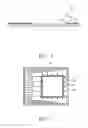
FIG. 1 is a schematic view of a transmitting substrate according to the present invention.
FIG. 2 is a schematic vertical view of the transmitting substrate according to FIG. 1.
FIG. 3 is a schematic view of the transmitting substrate combined with an image sensor according to the present invention.
FIG. 4 is a partial enlarged view of the packaged image sensor according to the present invention.
FIG. 5 is a schematic view of the protective structure according to a prior art.
FIG. 6 is a vertical view according to FIG. 5.
DETAILED DESCRIPTION OF THE PREFERRED EMBODIMENT
Please refer to FIGS. 1 to 4 for a preferred embodiment of the present invention. It is to be understood that the recited embodiment is for the purpose of illustration and not intended to limit the present invention with the discussed structure.
The flip chip packaging method that protects a sensing area of an image sensor from contamination according to the particular embodiment primarily comprises following steps:
a. providing a transmitting substrate 1 having a surface 11 with a predetermined area 12 defined thereon and making a metal layer 13 thereon which includes a circuit 131 and at least one enclosure encircling said predetermined area 12 made by screen printing, dispensing and depositing, wherein, according to this embodiment, the metal layer 13 has two enclosures 132, 133 wherein the enclosure 132 closely encloses the predetermined area 12 and the enclosure 133 encloses the enclosure 132 with an interval 134 spacing in between, as shown in FIG. 1 and FIG. 2.
b. providing an image sensor 2 mounted on the surface 11 of the transmitting substrate 1 and making the sensing area 21 thereof corresponding to said predetermined area 12 of the transmitting substrate 1 and making each bond pad 22 of the image sensor 2 electrically connected to the circuit 131 on the surface 11 of the transmitting substrate as shown in FIG.3 by means of reflow soldering, wherein, for instance, a method of electrically connecting the bond pad 22 to the circuit 131 may comprise: in Step a, after making a metal layer 13 on the surface 11 of the transmitting substrate 1, further plating a tin or tin alloy layer thereon to provide tin for forming an alloy with the gold surface of the bond pads 22 that renders final soldering connection between the bond pads 22 and the circuit 131 so that the interval between the transmitting substrate 1 and image sensor 2 can be minimized and the height of the enclosure 132 can also be increased; and wherein, the invention can be also embodied through normal soldering method by embedding tin balls; and
c. filling adhesive 24 around the image sensor 2 forming an airtight seal and after the adhesive 24 solidifies, the flip chip packaging of the image sensor is therefore achieved.
The method of the present invention is characterized by completing the prearranged circuit 131 and the two enclosure 132, 133 encircling the predetermined area simultaneously when making the metal layer 13 on the surface 11 of the transmitting substrate 1. When the filling adhesive 24 around the image sensor 2 on the surface 11 of the transmitting substrate 1 during flip chip packaging, as the enclosures 132, 133 encloses the predetermined area perform as protecting walls, the flowing adhesive 24 may be first barricaded before the outer enclosure 133 and if it keeps flowing toward the center of the sensor 2, it enters the interval 134 between the enclosures 132, 133 and is blocked before the inner enclosure 132. Thereupon, the adhesive 24 is efficiently kept away from flowing into the sensing area 21 of the image sensor 2 by the presence of the enclosures 132, 133.
Through above description of the embodiment, it is apparent that the disclosed invention is to simplify the flip chip packaging procedures and in turn reduce manufacturing expense by forming an enclosure synchronously while arranging a circuit on the surface of a transmitting substrate.
Claims
What is claimed is:1. A flip chip packaging method that protects a sensing area of an image sensor from contamination comprising the following steps:
a. providing a transmitting substrate having a surface with a predetermined area defined thereon and making a metal layer thereon which includes a circuit and at least one enclosure encircling said predetermined area;
b. providing an image sensor with the sensing area thereof deposited corresponding to said predetermined area and making each bond pad thereof electrically connected to the circuit on the surface of the transmitting substrate; and
c. filling adhesive around the image sensor forming an airtight seal, and after the adhesive solidifies, the flip chip packaging of the image sensor is therefore achieved.
2. The flip chip packaging method of claim 1, wherein in Step a, after a metal layer is formed on the surface of the transmitting substrate, a tin or tin alloy layer is next plated thereon.
Images & Drawings included:


Sources:
- United States Patent and Trademark Office - verify current appl. status at the USPTO↗
Recent applications in this class:
- » 20250063839 2025-02-20
IMAGING DEVICE AND ELECTRONIC DEVICE - » 20250056907 2025-02-13
LIGHT DETECTION DEVICE AND ELECTRONIC DEVICE - » 20240387578 2024-11-21
IMAGE SENSOR DEVICE AND METHOD OF FABRICATING THE SAME - » 20240363656 2024-10-31
IMAGING ELEMENT PACKAGE AND ELECTRONIC DEVICE - » 20240332326 2024-10-03
LIGHT DETECTING DEVICE, LIGHT DETECTING SYSTEM, AND FILTER ARRAY - » 20240321911 2024-09-26
IMAGE SENSOR AND MANUFACTURING METHOD THEREOF - » 20240282791 2024-08-22
DEVICE WITH A MULTIZONE REFLECTOR HAVING A DISCREET OPENING FOR A SENSOR - » 20240258346 2024-08-01
IMAGE SENSOR AND METHOD OF MANUFACTURING THE SAME - » 20240243144 2024-07-18
IMAGE SENSOR - » 20240243143 2024-07-18
Boron-Coated Back-Illuminated Image Sensor With Fluoride-Based Anti-Reflection Coating