Assembly of thin die coreless package
US20080160673A1
2008-07-03
11/648,120
2006-12-29
✅ Patent granted
US 7,666,714 B2
2010-02-23
-
-
David Vu | Earl N Taylor
2028-04-18
Abstract:
In one embodiment, a method comprises coupling a coreless substrate panel to a pressure cover plate of a carrier, applying flux to the coreless substrate panel, placing at least one die on the coreless substrate panel, reflowing solder onto the coreless substrate panel, defluxing the coreless substrate panel, underfilling the coreless substrate panel, and attaching at least one heat spreader to the coreless substrate panel.
Inventors:
- Rajashree Baskaran 16 🇺🇸 Seattle, WA, United States
- Charan Gurumurthy 26 🇺🇸 Higley, AZ, United States
- Daoqiang Lu 110 🇺🇸 Chandler, AZ, United States
Assignee:
- INTEL CORPORATION 47,158 🇺🇸 Santa Clara, CA, United States
Interested in similar patents?
Get notified when new applications in this technology area are published.
Classification:
H01L21/563 » CPC main
Processes or apparatus adapted for the manufacture or treatment of semiconductor or solid state devices or of parts thereof; Manufacture or treatment of semiconductor devices or of parts thereof the devices having at least one potential-jump barrier or surface barrier, e.g. PN junction, depletion layer or carrier concentration layer; Assembly of semiconductor devices using processes or apparatus not provided for in a single one of the subgroups - , e.g. sealing of a cap to a base of a container; Encapsulations, e.g. encapsulation layers, coatings Encapsulation of active face of flip-chip device, e.g. underfilling or underencapsulation of flip-chip, encapsulation preform on chip or mounting substrate
H01L21/561 » CPC further
Processes or apparatus adapted for the manufacture or treatment of semiconductor or solid state devices or of parts thereof; Manufacture or treatment of semiconductor devices or of parts thereof the devices having at least one potential-jump barrier or surface barrier, e.g. PN junction, depletion layer or carrier concentration layer; Assembly of semiconductor devices using processes or apparatus not provided for in a single one of the subgroups - , e.g. sealing of a cap to a base of a container; Encapsulations, e.g. encapsulation layers, coatings Batch processing
H01L21/568 » CPC further
Processes or apparatus adapted for the manufacture or treatment of semiconductor or solid state devices or of parts thereof; Manufacture or treatment of semiconductor devices or of parts thereof the devices having at least one potential-jump barrier or surface barrier, e.g. PN junction, depletion layer or carrier concentration layer; Assembly of semiconductor devices using processes or apparatus not provided for in a single one of the subgroups - , e.g. sealing of a cap to a base of a container; Encapsulations, e.g. encapsulation layers, coatings Temporary substrate used as encapsulation process aid
H01L21/6835 » CPC further
Processes or apparatus adapted for the manufacture or treatment of semiconductor or solid state devices or of parts thereof; Apparatus specially adapted for handling semiconductor or electric solid state devices during manufacture or treatment thereof; Apparatus specially adapted for handling wafers during manufacture or treatment of semiconductor or electric solid state devices or components ; Apparatus not specifically provided for elsewhere for supporting or gripping using temporarily an auxiliary support
H01L24/81 » CPC further
Arrangements for connecting or disconnecting semiconductor or solid-state bodies; Methods or apparatus related thereto; Methods for connecting semiconductor or other solid state bodies using means for bonding being attached to, or being formed on, the surface to be connected using a bump connector
H01L24/97 » CPC further
Arrangements for connecting or disconnecting semiconductor or solid-state bodies; Methods or apparatus related thereto; Batch processes at chip-level, i.e. with connecting carried out on a plurality of singulated devices, i.e. on diced chips the devices being connected to a common substrate, e.g. interposer, said common substrate being separable into individual assemblies after connecting
H01L2221/68354 » CPC further
Processes or apparatus adapted for the manufacture or treatment of semiconductor or solid state devices or of parts thereof covered by; Apparatus for handling semiconductor or electric solid state devices during manufacture or treatment thereof; Apparatus for handling wafers during manufacture or treatment of semiconductor or electric solid state devices or components; Apparatus not specifically provided for elsewhere for supporting or gripping using temporarily an auxiliary support used to support diced chips prior to mounting
H01L2221/68359 » CPC further
Processes or apparatus adapted for the manufacture or treatment of semiconductor or solid state devices or of parts thereof covered by; Apparatus for handling semiconductor or electric solid state devices during manufacture or treatment thereof; Apparatus for handling wafers during manufacture or treatment of semiconductor or electric solid state devices or components; Apparatus not specifically provided for elsewhere for supporting or gripping using temporarily an auxiliary support used as a support during manufacture of interconnect decals or build up layers
H01L2224/81001 » CPC further
Indexing scheme for arrangements for connecting or disconnecting semiconductor or solid-state bodies and methods related thereto as covered by; Methods for connecting semiconductor or other solid state bodies using means for bonding being attached to, or being formed on, the surface to be connected using a bump connector involving a temporary auxiliary member not forming part of the bonding apparatus
H01L2224/8121 » CPC further
Indexing scheme for arrangements for connecting or disconnecting semiconductor or solid-state bodies and methods related thereto as covered by; Methods for connecting semiconductor or other solid state bodies using means for bonding being attached to, or being formed on, the surface to be connected using a bump connector; Applying energy for connecting using a reflow oven
H01L2224/81815 » CPC further
Indexing scheme for arrangements for connecting or disconnecting semiconductor or solid-state bodies and methods related thereto as covered by; Methods for connecting semiconductor or other solid state bodies using means for bonding being attached to, or being formed on, the surface to be connected using a bump connector; Bonding techniques; Soldering or alloying Reflow soldering
H01L2224/8191 » CPC further
Indexing scheme for arrangements for connecting or disconnecting semiconductor or solid-state bodies and methods related thereto as covered by; Methods for connecting semiconductor or other solid state bodies using means for bonding being attached to, or being formed on, the surface to be connected using a bump connector; Post-treatment of the bump connector or bonding area Cleaning, e.g. oxide removal step, desmearing
H01L2924/014 » CPC further
Indexing scheme for arrangements or methods for connecting or disconnecting semiconductor or solid-state bodies as covered by; Alloys Solder alloys
H01L2924/14 » CPC further
Indexing scheme for arrangements or methods for connecting or disconnecting semiconductor or solid-state bodies as covered by; Details of semiconductor or other solid state devices to be connected; Device type Integrated circuits
H01L2224/81 » CPC further
Indexing scheme for arrangements for connecting or disconnecting semiconductor or solid-state bodies and methods related thereto as covered by; Methods for connecting semiconductor or other solid state bodies using means for bonding being attached to, or being formed on, the surface to be connected using a bump connector
H01L2224/97 » CPC further
Indexing scheme for arrangements for connecting or disconnecting semiconductor or solid-state bodies and methods related thereto as covered by; Batch processes at chip-level, i.e. with connecting carried out on a plurality of singulated devices, i.e. on diced chips the devices being connected to a common substrate, e.g. interposer, said common substrate being separable into individual assemblies after connecting
H01L2224/73203 » CPC further
Indexing scheme for arrangements for connecting or disconnecting semiconductor or solid-state bodies and methods related thereto as covered by; Means for bonding being of different types provided for in two or more of groups; Location after the connecting process on the same surface Bump and layer connectors
H01L2924/16152 » CPC further
Indexing scheme for arrangements or methods for connecting or disconnecting semiconductor or solid-state bodies as covered by; Details of package parts other than the semiconductor or other solid state devices to be connected; Cap; Shape Cap comprising a cavity for hosting the device, e.g. U-shaped cap
H01L2224/73253 » CPC further
Indexing scheme for arrangements for connecting or disconnecting semiconductor or solid-state bodies and methods related thereto as covered by; Means for bonding being of different types provided for in two or more of groups; Location after the connecting process on different surfaces Bump and layer connectors
H01L21/02 IPC
Processes or apparatus adapted for the manufacture or treatment of semiconductor or solid state devices or of parts thereof Manufacture or treatment of semiconductor devices or of parts thereof
Description
BACKGROUND
The subject matter described herein relates to the assembly of thin die coreless packages.
Electronic components, including integrated circuits, may be assembled into component packages by physically and electrically coupling them to a substrate. Thin dies exhibit performance advantages in some circumstances. Hence, techniques for the assembly of thin die packages find utility.
BRIEF DESCRIPTION OF THE DRAWINGS
The detailed description is described with reference to the accompanying figures.
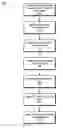
FIG. 1 is a flowchart illustrating operations in an embodiment of a method for assembly of thin die coreless IC packages.
FIG. 2A is a schematic illustration of an embodiment of a thin die coreless IC package.
FIGS. 2B-2D are schematic illustrations of an embodiment of a thin die coreless IC package during an assembly process.
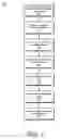
FIG. 3 is a flowchart illustrating operations in an embodiment of a method for assembly of thin die coreless IC packages.
FIGS. 4B-4E are schematic illustrations of an embodiment of a thin die coreless IC package during an assembly process.
DETAILED DESCRIPTION
Described herein are techniques for assembly of thin die coreless packages for integrated circuits. In the following description, numerous specific details are set forth to provide a thorough understanding of various embodiments. However, it will be understood by those skilled in the art that the various embodiments may be practiced without the specific details. In other instances, well-known methods, procedures, components, and circuits have not been illustrated or described in detail so as not to obscure the particular embodiments.
One embodiment of techniques for assembly of thin die coreless packages for integrated circuits will be described with reference to FIG. 1 and FIGS. 2A-2D. FIG. 1 is a flowchart illustrating operations in an embodiment of a method for assembly of thin die coreless integrated circuit (IC packages). FIG. 2A is a schematic illustration of an embodiment of a thin die coreless IC package. FIGS. 2B-2D are schematic illustrations of an embodiment of a thin die coreless IC package during an assembly process.
Referring first to FIG. 2A, in some embodiments a thin die coreless (TDCL) package architecture may comprise a thin die 210, a coreless substrate 215, a heat spreader, and a thermal interface material (TIM). In some embodiments, a coreless substrate may be obtained in panel form. Extra space may be provided between adjacent substrates. A substrate carrier 230 is provided. In some embodiments the substrate carrier 230 may be designed and fabricated. In the embodiment depicted in FIG. 2B, the substrate carrier 230 has a flat base and a pressure cover plate 240. The cover plate 240 includes a grid which will be pressed against the space between adjacent substrates to flatten the coreless substrates.
Referring to FIG. 1, at operation 105 a coreless substrate 215 is coupled to a pressure cover plate 240 of a substrate carrier 230. In some embodiments, the coreless substrate 215 may be in panel form. In some embodiments, the coreless substrate 215 provides a space between two or more adjacent substrates. In some embodiments, the carrier 230 comprises a flat base and a pressure cover plate, and the pressure cover plate 240 comprises a fine grid, which is pressed against space between adjacent substrates.
At operation 110 flux is applied to the coreless substrate panel 215. At operation 115 at least one die (210) is placed on the coreless substrate panel 215 (FIG. 2C). At operation 120 solder is reflowed onto the coreless substrate panel 215 (FIG. 2C). At operation 125 the coreless substrate panel 215 is defluxed (FIG. 2C). At operation 130 the coreless substrate panel 215 is underfilled.
At operation 135 at least one heat spreader 250 is attached to the coreless substrate panel (FIG. 2D). In some embodiments, attaching at least one heat spreader 250 to the coreless substrate panel 215 may include attaching one or more pressure clips 255 to apply bonding pressure to the heat spreader 250. The assembled chip packages may then be separated.
Another embodiment of techniques for assembly of thin die coreless packages for integrated circuits will be described with reference to FIG. 3 and FIGS. 4A-4E. FIG. 3 is a flowchart illustrating operations in an embodiment of a method for assembly of thin die coreless IC packages. FIG. 4A is a schematic illustration of an embodiment of a template for use in a thin die coreless IC package. FIGS. 4B-4E are schematic illustrations of an embodiment of a thin die coreless IC package during an assembly process.
Referring to FIG. 3, at operation 310 a template is formed. In some embodiments a template 405 may be fabricated with one or more shallow cavities for holding the dies 410. The dimensions and location of the cavities may be controlled with high precision. The template may comprise silicon. At operation 315 a die is positioned in at least one cavity of the template 405. In some embodiments all dies are positioned in the cavities of the template 405.
At operation 320 the die(s) are transferred to a die carrier 420. In some embodiments transferring the die(s) to a die carrier comprises coating the die carrier with a layer of a high temperature silicone-based tacky material and contacting the die carrier to the template (FIG. 4B). At operation 325 the die carrier 420 is positioned adjacent a substrate panel having printed flux thereon (FIG. 4B). The substrate panel may be positioned with a carrier 430 (FIG. 4C). In some embodiments carrier 430 comprises a flat base and a pressure cover plate, which may comprise a grid which is pressed against space between adjacent substrates.
At operation 330 solder is reflowed onto the coreless substrate panel 215 (FIG. 4D). At operation 335 the coreless substrate panel is defluxed (FIG. 4D). At operation 340 the coreless substrate panel is underfilled (FIG. 4D).
At operation 345 at least one heat spreader 450 is attached to the coreless substrate panel (FIG. 4E). In some embodiments, attaching at least one heat spreader 450 to the coreless substrate panel 415 may include attaching one or more pressure clips 455 to apply bonding pressure to the heat spreader 450. The assembled chip packages may then be separated.
In the description and claims, the terms coupled and connected, along with their derivatives, may be used. In particular embodiments, connected may be used to indicate that two or more elements are in direct physical or electrical contact with each other. Coupled may mean that two or more elements are in direct physical or electrical contact. However, coupled may also mean that two or more elements may not be in direct contact with each other, but yet may still cooperate or interact with each other.
Reference in the specification to “one embodiment” “some embodiments” or “an embodiment” means that a particular feature, structure, or characteristic described in connection with the embodiment is included in at least an implementation. The appearances of the phrase “in one embodiment” in various places in the specification may or may not be all referring to the same embodiment.
Although embodiments have been described in language specific to structural features and/or methodological acts, it is to be understood that claimed subject matter may not be limited to the specific features or acts described. Rather, the specific features and acts are disclosed as sample forms of implementing the claimed subject matter.
Claims
What is claimed is:1. A method, comprising:
coupling a coreless substrate panel to a pressure cover plate of a carrier; and
applying flux to the coreless substrate panel;
placing at least one die on the coreless substrate panel;
reflowing solder onto the coreless substrate panel;
defluxing the coreless substrate panel;
underfilling the coreless substrate panel; and
attaching at least one heat spreader to the coreless substrate panel.
2. The method of claim 1, wherein the coreless substrate is in panel form.
3. The method of claim 1, wherein the coreless substrate provides a space between two or more adjacent substrates.
4. The method of claim 3, wherein the carrier comprises a flat base and a pressure cover plate.
5. The method of claim 4, wherein the pressure cover plate comprises a fine grid, and is pressed against space between adjacent substrates.
6. The method of claim 1, wherein attaching at least one heat spreader to the coreless substrate panel comprises attaching one or more pressure clips to apply bonding pressure to the heat spreader.
7. The method of claim 1, further comprising separating at least one assembled chip package.
8. A method, comprising:
forming a template which comprises at least one cavity for holding a die;
positioning a die in at least one cavity of the template;
transferring the die from the template to a die carrier;
positioning the die carrier adjacent a substrate panel having printed flux;
reflowing solder on the substrate panel;
detaching the die carrier;
defluxing the substrate panel;
underfilling the substrate panel; and
attaching at least one heat spreader to the substrate panel.
9. The method of claim 8, wherein the template is formed from silicon.
10. The method of claim 8, wherein transferring the die from the template to a die carrier comprises:
coating the die carrier with a layer of a high temperature silicone-based tacky material;
contacting the die carrier to the template.
11. The method of claim 8, wherein the substrate provides a space between two or more adjacent substrates.
12. The method of claim 11, wherein the carrier comprises a flat base and a pressure cover plate.
13. The method of claim 12, wherein the pressure cover plate comprises a fine grid, and is pressed against space between adjacent substrates.
14. The method of claim 8, wherein attaching at least one heat spreader to the coreless substrate panel comprises attaching one or more pressure clips to apply bonding pressure to the heat spreader.
15. The method of claim 8, further comprising separating at least one assembled chip package.
Images & Drawings included:


Sources:
- United States Patent and Trademark Office - verify current appl. status at the USPTO↗
Recent applications in this class:
- » 20250293051 2025-09-18
PACKAGE STRUCTURE WITH UNDERFILL - » 20250266266 2025-08-21
MOLDED PACKAGES IN A MOLDED DEVICE - » 20250246445 2025-07-31
FLIP CHIP PACKAGE UNIT AND ASSOCIATED PACKAGING METHOD - » 20250157828 2025-05-15
SEMICONDUCTOR ASSEMBLIES WITH UNDERFILL SQUEEZE-UP, AND METHODS FOR MAKING THE SAME - » 20250118575 2025-04-10
INTEGRATED CIRCUIT PACKAGE AND METHOD OF FORMING THEREOF - » 20250096009 2025-03-20
LOW COST PACKAGE WARPAGE SOLUTION - » 20240395567 2024-11-28
SELECTIVE UNDERFILLING USING PRE-APPLIED THERMOSET ADHESIVE - » 20240387198 2024-11-21
Integrated Circuit Package and Method - » 20240339336 2024-10-10
SUBSTRATE HAVING UNDERFILL DAM AND SEMICONDUCTOR PACKAGE INCLUDING THE SAME, AND METHOD FOR MANUFACTURING THE SEMICONDUCTOR PACKAGE - » 20240312798 2024-09-19
SEMICONDUCTOR DIE PACKAGE WITH RING STRUCTURE
Recent applications for this Assignee:
- » 20250294866 2025-09-18
GATE CUT CONFINED WITHIN GATE TRENCH - » 20250294846 2025-09-18
BACKSIDE CROSS-COUPLE INTERCONNECTS - » 20250294835 2025-09-18
ELONGATED VERTICAL STRUCTURES OF CHANNEL MATERIALS - » 20250294827 2025-09-18
CO-INTEGRATION OF GATE-ALL-AROUND DEVICES WITH DIFFERENT NUMBERS OF NANORIBBONS - » 20250294818 2025-09-18
TRANSISTOR DESIGNS FOR FLOATING BODY MEMORY - » 20250294781 2025-09-18
MAGNETIC CORE INDUCTORS ON PACKAGE SUBSTRATES - » 20250294777 2025-09-18
INTEGRATED CIRCUIT DEVICE WITH MEMORY ARRAY AND SHARED GAIN ELEMENT - » 20250293985 2025-09-18
RECEIVER-BASED PRECISION CONGESTION CONTROL - » 20250293860 2025-09-18
PRESERVATION OF CONFIDENTIALITY AND INTEGRITY OF MODELS DURING EXECUTION - » 20250293706 2025-09-18
LOW-RANK DECOMPOSITION-BASED HARDWARE COMPRESSION OF MATRICES AND TENSORS