Low-thickness electronic module comprising a stack of electronic packages provided with connection balls
US20080170374A1
2008-07-17
11/910,433
2006-04-03
✅ Patent granted
US 8,243,468 B2
2012-08-14
WO; PCT/EP2006/061281; 20060403
WO; WO2006/103299; 20061005
Tuan T Dinh
2028-12-10
Abstract:
The invention relates to an electronic module (100) comprising a stack of n packages (10, 10a, 10b) of predetermined thickness E, which are provided on a lower surface with connection balls (12) of predetermined thickness eb, said connection balls being connected to a printed circuit (20, 20a, 20b) for interconnecting the package. The printed circuit is placed on the lower surface of the package level with the balls, is drilled with metallized holes (23), in which the balls (12) are located and to which they are connected, and has a thickness eci less than eb so as to obtain a module with a total thickness not exceeding n (E+10% eb).
Interested in similar patents?
Get notified when new applications in this technology area are published.
Classification:
H01L23/4985 » CPC main
Details of semiconductor or other solid state devices; Arrangements for conducting electric current to or from the solid state body in operation, e.g. leads, terminal arrangements ; Selection of materials therefor consisting of soldered constructions; Leads, on insulating substrates, Flexible insulating substrates
H01L23/3114 » CPC further
Details of semiconductor or other solid state devices; Encapsulations, e.g. encapsulating layers, coatings, e.g. for protection characterised by the arrangement or shape the device being completely enclosed the device being a chip scale package, e.g. CSP
H01L23/49816 » CPC further
Details of semiconductor or other solid state devices; Arrangements for conducting electric current to or from the solid state body in operation, e.g. leads, terminal arrangements ; Selection of materials therefor consisting of soldered constructions; Leads, on insulating substrates,; Additional leads joined to the metallisation on the insulating substrate, e.g. pins, bumps, wires, flat leads Spherical bumps on the substrate for external connection, e.g. ball grid arrays [BGA]
H01L23/5387 » CPC further
Details of semiconductor or other solid state devices; Arrangements for conducting electric current within the device in operation from one component to another, i.e. interconnections, e.g. wires, lead frames the interconnection structure between a plurality of semiconductor chips being formed on, or in, insulating substrates Flexible insulating substrates
H01L25/105 » CPC further
Assemblies consisting of a plurality of individual semiconductor or other solid state devices ; Multistep manufacturing processes thereof all the devices being of a type provided for in the same subgroup of groups - , e.g. assemblies of rectifier diodes the devices having separate containers the devices being of a type provided for in group
H05K3/3436 » CPC further
Apparatus or processes for manufacturing printed circuits; Assembling printed circuits with electric components, e.g. with resistor electrically connecting electric components or wires to printed circuits by soldering; Surface mounted components; Leadless components having an array of bottom contacts, e.g. pad grid array or ball grid array components
H01L2225/1064 » CPC further
Details relating to assemblies covered by the group but not provided for in its subgroups; All the devices being of a type provided for in the same subgroup of groups - the devices having separate containers the devices being of a type provided for in group the containers being in a stacked arrangement; Details of electrical connections between containers Electrical connections provided on a side surface of one or more of the containers
H01L2225/107 » CPC further
Details relating to assemblies covered by the group but not provided for in its subgroups; All the devices being of a type provided for in the same subgroup of groups - the devices having separate containers the devices being of a type provided for in group the containers being in a stacked arrangement; Details of electrical connections between containers Indirect electrical connections, e.g. via an interposer, a flexible substrate, using TAB
H01L2924/19041 » CPC further
Indexing scheme for arrangements or methods for connecting or disconnecting semiconductor or solid-state bodies as covered by; Details of hybrid assemblies other than the semiconductor or other solid state devices to be connected; Structure; Component type being a capacitor
H05K1/116 » CPC further
Printed circuits; Details; Printed elements for providing electric connections to or between printed circuits; Via connections; Lands around holes or via connections Lands, clearance holes or other lay-out details concerning the surrounding of a via
H05K1/116 » CPC further
Printed circuits; Details; Printed elements for providing electric connections to or between printed circuits; Via connections; Lands around holes or via connections Lands, clearance holes or other lay-out details concerning the surrounding of a via
H05K1/189 » CPC further
Printed circuits; Printed circuits structurally associated with non-printed electric components characterised by the use of a flexible or folded printed circuit
H05K1/189 » CPC further
Printed circuits; Printed circuits structurally associated with non-printed electric components characterised by the use of a flexible or folded printed circuit
H05K2201/09572 » CPC further
Indexing scheme relating to printed circuits covered by; Shape and layout; Shape and layout details of conductors; Conductive through-holes or vias Solder filled plated through-hole in the final product
H05K2201/09572 » CPC further
Indexing scheme relating to printed circuits covered by; Shape and layout; Shape and layout details of conductors; Conductive through-holes or vias Solder filled plated through-hole in the final product
H05K2201/09663 » CPC further
Indexing scheme relating to printed circuits covered by; Shape and layout; Shape and layout details of conductors covering at least two types of conductors provided for in - Divided layout, i.e. conductors divided in two or more parts
H05K2201/09663 » CPC further
Indexing scheme relating to printed circuits covered by; Shape and layout; Shape and layout details of conductors covering at least two types of conductors provided for in - Divided layout, i.e. conductors divided in two or more parts
H05K2203/041 » CPC further
Indexing scheme relating to apparatus or processes for manufacturing printed circuits covered by; Soldering or other types of metallurgic bonding Solder preforms in the shape of solder balls
H05K2203/041 » CPC further
Indexing scheme relating to apparatus or processes for manufacturing printed circuits covered by; Soldering or other types of metallurgic bonding Solder preforms in the shape of solder balls
H05K2203/0455 » CPC further
Indexing scheme relating to apparatus or processes for manufacturing printed circuits covered by; Soldering or other types of metallurgic bonding PTH for surface mount device [SMD], e.g. wherein solder flows through the PTH during mounting
H05K2203/0455 » CPC further
Indexing scheme relating to apparatus or processes for manufacturing printed circuits covered by; Soldering or other types of metallurgic bonding PTH for surface mount device [SMD], e.g. wherein solder flows through the PTH during mounting
Y02P70/50 » CPC further
Climate change mitigation technologies in the production process for final industrial or consumer products Manufacturing or production processes characterised by the final manufactured product
Y02P70/50 » CPC further
Climate change mitigation technologies in the production process for final industrial or consumer products Manufacturing or production processes characterised by the final manufactured product
H01L2924/0002 » CPC further
Indexing scheme for arrangements or methods for connecting or disconnecting semiconductor or solid-state bodies as covered by; Technical content checked by a classifier Not covered by any one of groups , and
H01L2924/00 » CPC further
Indexing scheme for arrangements or methods for connecting or disconnecting semiconductor or solid-state bodies as covered by
H05K7/00 IPC
Constructional details common to different types of electric apparatus
H05K7/00 IPC
Constructional details common to different types of electric apparatus
Description
The invention relates to an electronic module of small thickness, which comprises a stack of electronic packages.
These packages comprise a printed circuit with at least one chip, encapsulated by a protective resin, and are provided on their lower surface with connection balls. These are for example packages of the BGA (Ball Grid Array) or FBGA (Fine Ball Grid Array) type.
They are stacked to form an electronic module. FIG. 1a shows, in cross section, a known electronic module 100 comprising two packages 10a, 10b. It includes, for each package, a circuit 20 for interconnecting the package shown in FIG. 1b seen from above, the area of which is the same size as that of the package, and the tracks 21 of which connects pads 22 positioned facing the balls 12, at the edges of the circuit. A central band, with no connections or pads, corresponds to the central band of the lower surface of the package that protects the wires of the wiring connecting the balls to the printed circuit of the package. These circuits 20 are connected together via their edges, in this case by a metal bus 30 located on one side of the module. Connection balls 12 are placed beneath the lower interconnection circuit 10a for connecting the module 100 to an interconnection substrate 200. An insulating lacquer 14 is placed beneath the lower surface of body 11 of the package.
At the present time, electronic modules are subject to thickness and area constraints—a module with two packages must not exceed 2.7 mm in thickness and its area must not exceed that of a package. A package body 11 typically has a thickness of 0.8 mm, a printed interconnection circuit 20 has a thickness of 0.15 mm and a connection ball 12 has a thickness of 0.4 mm. The overall thickness is 3.1 mm, and therefore exceeds the required limit.
The object of the invention is to propose an electronic module that meets these thickness and area constraints.
One subject of the invention is an electronic module comprising a stack of n packages of predetermined thickness E, where n>1, each package being provided on the lower surface of the body of the package with connection balls of predetermined thickness eb and, connected to these balls, with a printed circuit for interconnecting the package. It is mainly characterized in that the printed circuit is placed on the lower surface of the body of the package level with the balls, is drilled with metallized holes, in which the balls are located and to which they are connected, and has a thickness eci less than eb so as to obtain a module with a total thickness not exceeding n (E+10% eb).
In this way, the interconnection circuit of the package is integrated between the balls. It therefore does not add thickness to the package, nor does it increase its area. The thickness of each package is thus reduced by the thickness of the printed connection circuit.
According to one feature of the invention, the electronic module includes a lateral element for connecting the drilled circuits together and the stack has a lower package and upper packages, the drilled printed circuit of the lower package includes at least one ball not connected to the lower package and intended for connecting an upper package to an interconnection substrate of the module, via the drilled printed circuit and the lateral connection element.
According to a first embodiment of the invention, the drilled printed circuits are connected together by a metal bus.
According to another embodiment, at least two drilled printed circuits are connected together by a lateral connection element which forms, with these drilled printed circuits, a flexible circuit called a flex circuit.
This flex circuit may be in the form of a concertina.
Advantageously, the module includes at least one capacitor film placed on and/or beneath each package.
Preferably, the holes are approximately circular and have a diameter dp equal to or greater than the diameter eb of the balls, so that the balls pass through the drilled printed circuit before they are connected, or less than the diameter eb of the balls, so as to at least reduce the routable area of the printed circuit.
Another subject of the invention is an electronic package of predetermined thickness E, provided on the lower surface of the body of the package with connection balls of predetermined thickness eb, characterized in that it includes a printed circuit for interconnecting the package and placed on the lower surface of the body of the package level with the balls, which circuit is drilled with approximately circular metallized holes in which the balls are located and to which they are connected, and has a thickness eci less than eb so as to obtain a package with a total thickness not exceeding E+10% eb.
Preferably, the drilled printed circuit includes at least one ball not connected to the package or a soldered hole not connected to the package.
According to one feature of the invention, the holes are approximately circular and have a diameter dp equal to or greater than the diameter eb of the balls, or less than the diameter eb of the balls for the reasons mentioned above.
Other features and advantages of the invention will become apparent on reading the following detailed description, by way of nonlimiting example and with reference to the appended drawings in which:
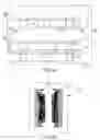
FIGS. 1a and 1b, already described, show schematically a known electronic module comprising two packages, seen in cross section, and a known package interconnection circuit seen from above;
FIGS. 2a and 2b show schematically an electronic package according to the invention before connection, seen in cross section, and a package interconnection circuit according to the invention seen from above;
FIGS. 3a and 3b show schematically two steps of an example of one way of producing an electronic package according to the invention, when the holes in the interconnection circuit of the package are smaller than the balls, before the balls have been connected (FIG. 3a) and after they have been connected (FIG. 3b);
FIGS. 4a, 4b and 4c show schematically examples of the shape of metallization collars of the holes;
FIG. 5 shows schematically an example of a first embodiment of an electronic module according to the invention comprising two packages, after connection, seen in cross section;
FIGS. 6a and 6b show schematically two examples of a second embodiment of an electronic module according to the invention after connection, seen in cross section, comprising two and three packages respectively; and
FIG. 7 shows schematically an electronic module according to the invention comprising two packages, which is placed on a module interconnection substrate, after connection.
From one figure to another, the same elements are identified by the same references.
The example of a package 10 represented in cross section in FIG. 2a includes the same elements as that described in relation to FIG. 1a, namely connection balls 12 and a printed circuit 20 for interconnecting the package, adhesively bonded to the lower surface of the package body 11, in this case to the lacquer 14, by means of a resin (not shown in the figure). According to the invention, this circuit 20 is drilled with holes 23 shown in FIG. 2b and placed opposite the balls 12. The pads 22 of the interconnection circuit of the prior art, described in relation to FIG. 1b, have been replaced by metallized holes 23.
These holes are metallized and have a conducting collar 24, the balls being connected to the holes by soldering.
According to a first embodiment of a package illustrated in FIG. 2a, these holes are approximately circular of diameter dp and are preferably slightly larger than the balls so that the latter pass easily through the circuit before the balls are connected to the circuit. Thus, dp≧eb.
Initially, the balls have a thickness eb of about 0.4 mm for example. Upon connecting them to the metallized holes, the thickness of the balls, which maintain a constant volume, decreases: it may then possibly be compensated for by supplying, during soldering, additional material so as to maintain the initial thickness of the balls. The balls thus have a constant thickness. The material added is that used for the balls, such as for example a lead-free alloy, such as a tin/copper/silver alloy.
The larger the holes, the smaller the routable area of the circuit, which is a drawback. The term “routable area” is understood to mean the area that includes the connection tracks denoted by 21 in FIGS. 1b and 2b.
According to another embodiment of a package, which may remedy this problem of a reduced routable area and is illustrated in FIGS. 3a and 3b for one ball, the circular holes are smaller than the balls. Therefore dp<eb. Before the balls are connected to the metallized holes, the drilled circuit 20 is placed beneath the balls 12, as shown in FIG. 3a. During connection of the balls to the circuit, for example by soldering, the balls 12, which deform by capillary effect, also pass through the circuit 20 and create a hemispherical region 120 beneath the circuit 20, as shown in FIG. 3b. By deforming, they attract with them the body 11 of the package, which “descends”—the final height H, equal to that of the connected ball (=A+B) added to that of the drilled circuit (=hci), is equal to or less than the initial thickness of the ball eb within a margin of tolerance of about 10%. Overall, the height H is less than eb(1+10%).
The following results are obtained for an initial ball thickness eb of 420 μm and hci=100 μm: H=439 μm, A=244 μm and B=95 μm.
Therefore H<eb(1+10%). The total thickness E of the package is consequently less than E+10% eb.
The collar is for example circular, as shown in FIG. 4a, but it may have another shape. Since the second embodiment of the package is based on the capillary effect, this effect can be accentuated by choosing a collar in the form of two parts on either side of the hole, or in the form of quarters, shown in FIGS. 4b and 4c respectively, or more generally in a form having one part of the circular collar.
According to a first embodiment of a module, one example of which with two packages is shown in FIG. 5, the module 100 according to the invention includes a lateral element 30 for connecting the drilled circuits together, in this case a metal bus.
According to another embodiment of a module, one example of which, again with two packages, is shown in FIG. 6a, the module 100 according to the invention includes a lateral element 30 for connecting the drilled circuits together, which forms with these drilled circuits a single flexible circuit called a flex circuit.
The printed circuit 20 may be made from a single part or from two parts. When it is made from two parts, there are then two flex circuits located on either side of the module. When the module comprises n packages, where n>2, a flex circuit in the form of a concertina can then be used to connect in succession the n packages, as illustrated in FIG. 6b for three packages 10a, 10b and 10c. The flex circuit is then formed from printed circuits 20a, 20b and 20c and lateral connection elements 30a and 30b.
Preferably, a capacitor film 40 of small thickness (between 2 and 80 μm), in order to preserve the integrity of the signals transmitted by the connection elements, is placed beneath the balls and the package lying beneath these balls. This film may also be located on the package so as to have one capacitor film per package. This film may also be located between the balls 12a of the lower package and an interconnection substrate of the module. Finally, this film 40 may be located on and/or beneath each package 10. FIG. 6b shows a package 10c with a film 40 located beneath the balls 12c, and a package 10a with a film 40 located on the body 11a of the package.
The module according to the invention is intended to be placed on a substrate for interconnecting the module. The balls of the lower package allow the lower package to be connected to this substrate.
According to the invention, the drilled circuit 20a of the lower package 10a furthermore includes at least one ball 12s not connected to the lower package by a pad 13, as indicated in FIGS. 5, 6a and 7. This additional ball 12s allows the substrate 200 (FIG. 7) to be connected to an upper package 10b via the lower drilled circuit 20a and the lateral connection element 30 whether this be a metal bus or part of a flex circuit, or some other element. This ball 12s is used to convey a select signal, such as a CS (Chip Select), CKE (Clock Enable) or ODT (On Die Termination) signal, or any other signal. When several signals have to be sent to the same package, the lower drilled circuit has as many additional balls as there are signals. This number of balls is of course increased by the number of packages to be addressed. The lower drilled circuit finally has (n−1)m balls 12s in addition, n being the number of packages and m the number of signals. These balls 12s may be replaced with holes not connected to the lower package, without balls but soldered with solder identical to that of the balls. These soldered holes 12t, one example of which is shown in FIG. 7, are preferably smaller than the other holes—for example, they have a diameter of about 0.1 mm.
The following results were obtained for a module according to the first embodiment: its thickness does not exceed 2.4 mm (n×1.2 mm, here with n=2, the balls for connecting to the substrate 200 becoming unnecessary) instead of 3.1 mm in the case of the module of the prior art; nor does its area exceed that of a package.
Examples have been presented with two packages, but the module according to the invention may have three, four or more packages.
Claims
1. An electronic module comprising:
a stack of n packages of predetermined thickness E, where n>1, each package being provided on the lower surface of the body of the package with connection balls of predetermined thickness eb and, connected to the balls, with a printed circuit for interconnecting the package, which is placed on the lower surface of the body of the package level with the balls, which is drilled with metallized holes, in which the balls are located and to which they are connected, and has a thickness eci less than eb so as to obtain a module with a total thickness not exceeding n (E+10% eb), including a lateral element for connecting the drilled circuits together and wherein the stack has a lower package and upper packages, the drilled printed circuit of the lower package includes at least one ball or a soldered hole not connected to the lower package to connect an upper package to an interconnection substrate of the module, via the drilled printed circuit and the lateral connection element.
2. The electronic module as claimed in claim 1, wherein the printed interconnection circuit of the package has an area substantially of the same size as that of the package.
3. The electronic module as claimed in claim 1, wherein the lateral element is a metal bus.
4. The electronic module as claimed in claim 1, wherein the lateral connection element forms, with these drilled printed circuits, a flexible circuit.
5. The electronic module as claimed claim 4, wherein at least three drilled printed circuits are connected together by a flex circuit in the form of a concertina.
6. The electronic module as claimed in claim 1, including at least one capacitor film placed on and/or beneath each package.
7. The electronic module as claimed in claim 1, wherein the balls connected to the holes have a constant thickness eb.
8. The electronic module as claimed in claim 1, wherein the holes are approximately circular and have a diameter dp equal to or greater than the diameter eb of the balls.
9. The electronic module as claimed in claim 1, wherein the holes are approximately circular and have a diameter dp less than the diameter eb of the balls.
10. The electronic module as claimed in claim 1, wherein the holes are metallized as a circular collar or in two parts or in quarters.
11. The electronic module as claimed in claim 1, wherein the packages are packages of the BGA or FBGA type.
12. An electronic package of predetermined thickness E, provided on the lower surface of the body of the package with connection balls of predetermined thickness eb before connection, including a printed circuit for interconnecting the package and placed on the lower surface of the body of the package level with the balls, wherein which circuit is drilled with approximately circular metallized holes with a diameter dp equal to or greater than the diameter eb of the balls, in which the balls are located and to which the balls are connected, and has a thickness eci less than eb so that, after connection, the total thickness of the package, of the balls and of the interconnection circuit does not exceed E+10% eb.
13. The electronic package as claimed in claim 12, wherein the holes are metallized as a circular collar or in two parts or in quarters.
14. The electronic package as claimed in claim 12, wherein the printed interconnection circuit of the package has an area approximately the same size as that of the package.
15. The electronic package as claimed in claim 12, wherein the drilled printed circuit includes at least one ball not connected to the package or at least one soldered hole not connected to the package.
Images & Drawings included:


Sources:
- United States Patent and Trademark Office - verify current appl. status at the USPTO↗
Recent applications in this class:
- » 20250210505 2025-06-26
STRETCHABLE DEVICE - » 20250105131 2025-03-27
FLEXIBLE INTERPOSER - » 20250038099 2025-01-30
POWER SEMICONDUCTOR INTEGRATED UNIT AND POWER CONVERTER CIRCUIT STRUCTURE THEREOF, AND LOOP STRUCTURE WITH INTEGRATED UNITS CONNECTED IN PARALLEL - » 20240371744 2024-11-07
ARRAY SUBSTRATE, DISPLAY PANEL AND DISPLAY DEVICE - » 20240363519 2024-10-31
SEMICONDUCTOR DEVICE WITH RIGID-FLEX SUB-ASSEMBLY AND METHOD THEREFOR - » 20240347440 2024-10-17
Omnidirectional flexible light emitting device - » 20240321721 2024-09-26
STRETCHABLE DEVICE - » 20240290711 2024-08-29
ELECTRONIC DEVICE - » 20240178124 2024-05-30
Embedded Die Package - » 20240096779 2024-03-21
FLEXIBLE PACKAGE
Recent applications for this Assignee:
- » 20110312132 2011-12-22
Method for positioning chips during the production of a reconstituted wafer - » 20110247210 2011-10-13
Process for the wafer-scale fabrication of electronic modules for surface mounting - » 20100276081 2010-11-04
Method of interconnecting electronic wafers - » 20100276081 2010-11-04
Method of interconnecting electronic wafers - » 20090260228 2009-10-22
Process for the vertical interconnection of 3D electronic modules by vias - » 20090209052 2009-08-20
Process for the collective fabrication of 3D electronic modules - » 20090209052 2009-08-20
Process for the collective fabrication of 3D electronic modules - » 20080316727 2008-12-25
3D electronic module - » 20080289174 2008-11-27
Process for the collective fabrication of 3D electronic modules - » 20080289174 2008-11-27
Process for the collective fabrication of 3D electronic modules