ESD protection scheme for semiconductor devices having dummy pads
US20080173945A1
2008-07-24
11/655,896
2007-01-22
Abstract:
A semiconductor device formed in a semiconductor substrate for dissipating electrostatic discharge and/or accumulated charge in an integrated circuit is provided. In one embodiment, the device comprises a semiconductor substrate; a plurality of layers of metal lines formed overlying the substrate; a plurality of via plugs through intermetal dielectric layers between the layers of metal lines and wherein the via plugs interconnect the metal lines; and a dummy pad formed over the plurality of layers of metal lines, the dummy pad having a diode connected thereto and to ground for providing a discharge path for the electrostatic discharge and/or accumulated charge.
Inventors:
- Jian-Hsing LEE 16 🇹🇼 Hsinchu, Taiwan
- Yu-Chang Lin 55 🇹🇼 Hsinchu, Taiwan
- Yu-Ting Lin 7 🇹🇼 Hsinchu, Taiwan
- Yi-Hsun Wu 8 🇹🇼 Hsinchu, Taiwan
- Yan-Chih Jiang 1 🇹🇼 Jhubei City, Taiwan
- Shih-Hsorng Shen 5 🇹🇼 Hsinchu, Taiwan
- Yun-Sheng Huang 1 🇹🇼 Hsinchu, Taiwan
Assignee:
- TAIWAN SEMICONDUCTOR MANUFACTURING CO., LTD. 4,203 🇹🇼 Hsin-Chu, Taiwan
Interested in similar patents?
Get notified when new applications in this technology area are published.
Classification:
H01L23/585 » CPC further
Details of semiconductor or other solid state devices; Structural electrical arrangements for semiconductor devices not otherwise provided for, e.g. in combination with batteries comprising conductive layers or plates or strips or rods or rings
H01L24/11 » CPC further
Arrangements for connecting or disconnecting semiconductor or solid-state bodies; Methods or apparatus related thereto; Means for bonding being attached to, or being formed on, the surface to be connected, e.g. chip-to-package, die-attach, "first-level" interconnects; Manufacturing methods related thereto; Bump connectors ; Manufacturing methods related thereto Manufacturing methods
H01L2224/0554 » CPC further
Indexing scheme for arrangements for connecting or disconnecting semiconductor or solid-state bodies and methods related thereto as covered by; Means for bonding being attached to, or being formed on, the surface to be connected, e.g. chip-to-package, die-attach, "first-level" interconnects; Manufacturing methods related thereto; Bonding areas; Manufacturing methods related thereto; Structure, shape, material or disposition of the bonding areas prior to the connecting process of an individual bonding area External layer
H01L2224/05573 » CPC further
Indexing scheme for arrangements for connecting or disconnecting semiconductor or solid-state bodies and methods related thereto as covered by; Means for bonding being attached to, or being formed on, the surface to be connected, e.g. chip-to-package, die-attach, "first-level" interconnects; Manufacturing methods related thereto; Bonding areas; Manufacturing methods related thereto; Structure, shape, material or disposition of the bonding areas prior to the connecting process of an individual bonding area; External layer Single external layer
H01L23/60 » CPC main
Details of semiconductor or other solid state devices; Structural electrical arrangements for semiconductor devices not otherwise provided for, e.g. in combination with batteries Protection against electrostatic charges or discharges, e.g. Faraday shields
H01L2924/14 » CPC further
Indexing scheme for arrangements or methods for connecting or disconnecting semiconductor or solid-state bodies as covered by; Details of semiconductor or other solid state devices to be connected; Device type Integrated circuits
H01L2924/00 » CPC further
Indexing scheme for arrangements or methods for connecting or disconnecting semiconductor or solid-state bodies as covered by
H01L2224/05599 » CPC further
Indexing scheme for arrangements for connecting or disconnecting semiconductor or solid-state bodies and methods related thereto as covered by; Means for bonding being attached to, or being formed on, the surface to be connected, e.g. chip-to-package, die-attach, "first-level" interconnects; Manufacturing methods related thereto; Bonding areas; Manufacturing methods related thereto; Structure, shape, material or disposition of the bonding areas prior to the connecting process of an individual bonding area; External layer Material
H01L2224/0555 » CPC further
Indexing scheme for arrangements for connecting or disconnecting semiconductor or solid-state bodies and methods related thereto as covered by; Means for bonding being attached to, or being formed on, the surface to be connected, e.g. chip-to-package, die-attach, "first-level" interconnects; Manufacturing methods related thereto; Bonding areas; Manufacturing methods related thereto; Structure, shape, material or disposition of the bonding areas prior to the connecting process of an individual bonding area; External layer Shape
H01L2924/00014 » CPC further
Indexing scheme for arrangements or methods for connecting or disconnecting semiconductor or solid-state bodies as covered by; Technical content checked by a classifier the subject-matter covered by the group, the symbol of which is combined with the symbol of this group, being disclosed without further technical details
H01L2224/0556 » CPC further
Indexing scheme for arrangements for connecting or disconnecting semiconductor or solid-state bodies and methods related thereto as covered by; Means for bonding being attached to, or being formed on, the surface to be connected, e.g. chip-to-package, die-attach, "first-level" interconnects; Manufacturing methods related thereto; Bonding areas; Manufacturing methods related thereto; Structure, shape, material or disposition of the bonding areas prior to the connecting process of an individual bonding area; External layer Disposition
H01L21/00 IPC
Processes or apparatus adapted for the manufacture or treatment of semiconductor or solid state devices or of parts thereof
Description
BACKGROUND
The present invention relates generally to protection schemes for semiconductor devices from ESD (electrostatic discharge) and/or accumulated charges, and more particularly, to protection schemes for semiconductor devices having dummy pads from ESD and/or accumulated charges.
Isolated or dummy bond pads having solder balls formed thereon are often employed in the fabrication of semiconductor devices for improving the mechanical robustness of these devices. These dummy pads are isolated and are often not electrically connected to any circuit. However, accumulated charges or ESD often accumulate on these dummy pads and as a result discharge to neighboring devices, thereby damaging these devices or the top metal lines in the devices.
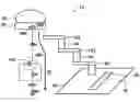
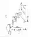
This problem is illustrated in FIG. 1. FIG. 1 shows a cross-sectional view of a semiconductor device 10 having a plurality of metal lines M1, M2, M3 formed overlying a substrate and a plurality of via plugs 40 through intermetal dielectric layers (not shown) formed between the layers of metal lines. A dummy pad 20 having a solder ball 30 formed thereon is positioned above a top most metal line M3. When accumulated charges or ESD 70 build up on dummy pad 20, they discharge to ground thereby damaging an internal circuit 60 in an active area 50 of the semiconductor device 10.
For these reasons and other reasons that will become apparent upon reading the following detailed description, there is a need for a protection scheme for semiconductor devices having dummy pads from ESD and/or accumulated charges.
SUMMARY
The present invention is directed to a semiconductor device formed in a semiconductor substrate for dissipating electrostatic discharge and/or accumulated charge in an integrated circuit. In one embodiment, the device comprises a semiconductor substrate; a plurality of layers of metal lines formed overlying the substrate; a plurality of via plugs through intermetal dielectric layers between the layers of metal lines and wherein the via plugs interconnect the metal lines; and a dummy pad formed over the plurality of layers of metal lines, the dummy pad having a diode connected thereto and to ground for providing a discharge path for the electrostatic discharge and/or accumulated charge.
In another embodiment, the device comprises a semiconductor substrate; a plurality of layers of metal lines formed overlying the substrate; a plurality of via plugs through intermetal dielectric layers between the layers of metal lines and wherein the via plugs interconnect the metal lines; and a dummy pad formed over the plurality of layers of metal lines, the dummy pad having a gate-grounded NMOS (ggNMOS) connected thereto, the drain being connected to the dummy pad and the gate and source being connected to ground for providing a discharge path for the electrostatic discharge and/or accumulated charge.
In yet another embodiment, the device comprises a semiconductor substrate; a plurality of layers of metal lines formed overlying the substrate; a plurality of via plugs through intermetal dielectric layers between the layers of metal lines and wherein the via plugs interconnect the metal lines; and a dummy pad formed over the plurality of layers of metal lines, the dummy pad comprising: a gate-grounded NMOS (ggNMOS), the drain being connected to the dummy pad and the gate and source being connected to ground; and a diode connected to the dummy pad and to ground for providing a discharge path for the electrostatic discharge and/or accumulated charge.
BRIEF DESCRIPTION OF THE DRAWINGS
The features, aspects, and advantages of the present invention will become more fully apparent from the following detailed description, appended claims, and accompanying drawings in which:
FIG. 1 is a cross-sectional view of a semiconductor device with dummy pads showing a discharge path of accumulated charge or electrostatic discharge from the dummy pad to an integrated circuit.
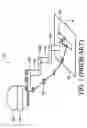
FIG. 2A is a cross-sectional view of a semiconductor device with dummy pads having an ESD protection scheme showing a discharge path of accumulated charge or electrostatic discharge from the dummy pad to ground, according to one embodiment of the present invention.
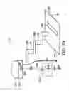
FIG. 2B is a cross-sectional view of a semiconductor device with dummy pads having an ESD protection scheme showing a discharge path of accumulated charge or electrostatic discharge from the dummy pad to ground, according to another embodiment of the present invention.
DETAILED DESCRIPTION
In the following description, numerous specific details are set forth to provide a thorough understanding of the present invention. However, one having an ordinary skill in the art will recognize that the invention can be practiced without these specific details. In some instances, well-known structures and processes have not been described in detail to avoid unnecessarily obscuring the present invention.
A first embodiment of the present invention will now be described with reference to FIG. 2A.
FIG. 2A is a cross-sectional view of a semiconductor device with dummy pads having an ESD protection scheme showing a discharge path of accumulated charge or electrostatic discharge from the dummy pad to ground, according to one embodiment of the present invention. The semiconductor device 12 has a plurality of metal lines M1, M2, M3 formed overlying a substrate and a plurality of via plugs 40 through intermetal dielectric layers (not shown) formed between the layers of metal lines, the via plugs 40 interconnecting the metal lines. A dummy pad 20 having a solder ball 30 formed thereon is positioned above the top most metal line M3. The protection scheme according to this embodiment comprises a diode 90 connected between the dummy pad 20 and ground. The cathode of the diode 90 is connected to the dummy pad 20 and the anode of the diode 90 is connected to ground. In one embodiment, the diode is a reverse diode. The purpose of the diode 90 is to gradually discharge the charges accumulated on dummy pad 20 and to avoid damage to an internal circuit 60. Instead of accumulated charges or ESD 95 built up on dummy pad 20 discharging to ground by way of the plurality of metal lines and vias damaging circuit 60 in an active area 50, the protection scheme of the present invention provides a low resistance discharge path for these harmful charges.
A second embodiment of the present invention will now be described with reference to FIG. 2B.
FIG. 2B is a cross-sectional view of a semiconductor device with dummy pads having an ESD protection scheme showing a discharge path of accumulated charge or electrostatic discharge from the dummy pad to ground, according to another embodiment of the present invention. The protection scheme according to this embodiment comprises a gate-grounded NMOS (ggNMOS) transistor 100 connected between the dummy pad 20 and ground. The ggNMOS 100 has a drain connected to the dummy pad 20 and a gate and a source both connected to ground. When an accumulated charge or ESD 95 accumulates on dummy pad 20, the charge is released through the ggNMOS. Therefore, the ESD charge is not applied to the circuit 60, and the circuit is protected.
In another embodiment, the protection scheme can comprise of both a diode and a ggNMOS transistor connected between the dummy pad and ground to provide a discharge path to ground away from the circuit to be protected.
In the preceding detailed description, the present invention is described with reference to specifically exemplary embodiments thereof. It will, however, be evident that various modifications, structures, and changes may be made thereto without departing from the broader spirit and scope of the present invention, as set forth in the claims. The specification and drawings are, accordingly, to be regarded as illustrative and not restrictive. It is understood that the present invention is capable of using various other combinations and environments and is capable of changes or modifications within the scope of the inventive concept as expressed herein.
Claims
What is claimed is:1. A semiconductor device formed in a semiconductor substrate for protecting an integrated circuit from electrostatic discharge and/or accumulated charge, the device comprising:
a semiconductor substrate;
a plurality of layers of metal lines formed overlying the substrate;
a plurality of via plugs through intermetal dielectric layers between the layers of metal lines and wherein the via plugs interconnect the metal lines; and
a dummy pad formed over the plurality of layers of metal lines, the dummy pad having a diode connected thereto and to ground for providing a discharge path for the electrostatic discharge and/or accumulated charge.
2. The semiconductor device of claim 1, wherein the cathode of the diode is connected to the dummy pad and the anode of the diode is connected to ground.
3. The semiconductor device of claim 1, wherein the diode is a reverse diode.
4. A semiconductor device formed in a semiconductor substrate for protecting an integrated circuit from electrostatic discharge and/or accumulated charge, the device comprising:
a semiconductor substrate;
a plurality of layers of metal lines formed overlying the substrate;
a plurality of via plugs through intermetal dielectric layers between the layers of metal lines and wherein the via plugs interconnect the metal lines; and
a dummy pad formed over the plurality of layers of metal lines, the dummy pad having a gate-grounded NMOS (ggNMOS) connected thereto, the drain being connected to the dummy pad and the gate and source being connected to ground for providing a discharge path for the electrostatic discharge and/or accumulated charge.
5. A semiconductor device formed in a semiconductor substrate for protecting an integrated circuit from electrostatic discharge and/or accumulated charge, the device comprising:
a semiconductor substrate;
a plurality of layers of metal lines formed overlying the substrate;
a plurality of via plugs through intermetal dielectric layers between the layers of metal lines and wherein the via plugs interconnect the metal lines; and
a dummy pad formed over the plurality of layers of metal lines, the dummy pad comprising:
a gate-grounded NMOS (ggNMOS), the drain being connected to the dummy pad and the gate and source being connected to ground; and
a diode connected to the dummy pad and to ground for providing a discharge path for the electrostatic discharge and/or accumulated charge.
6. The semiconductor device of claim 5, wherein the cathode of the diode is connected to the dummy pad and the anode of the diode is connected to ground.
7. The semiconductor device of claim 5, wherein diode is a reverse diode.
8. A method for forming a semiconductor device in a semiconductor substrate for protecting an integrated circuit from electrostatic discharge and/or accumulated charge, the method comprising:
providing a semiconductor substrate;
forming a plurality of layers of metal lines overlying the substrate;
forming a plurality of via plugs through intermetal dielectric layers between the layers of metal lines and wherein the via plugs interconnect the metal lines; and
providing a dummy pad over the plurality of layers of metal lines, the dummy pad having a diode connected thereto and to ground for providing a discharge path for the electrostatic discharge and/or accumulated charge.
9. The method of claim 8, wherein the cathode of the diode is connected to the dummy pad and the anode of the diode is connected to ground.
10. The method of claim 1, wherein the diode is a reverse diode.
11. A method for forming a semiconductor device in a semiconductor substrate for protecting an integrated circuit from electrostatic discharge and/or accumulated charge, the method comprising:
providing a semiconductor substrate;
forming a plurality of layers of metal lines overlying the substrate;
forming a plurality of via plugs through intermetal dielectric layers between the layers of metal lines and wherein the via plugs interconnect the metal lines; and
providing a dummy pad over the plurality of layers of metal lines, the dummy pad having a gate-grounded NMOS (ggNMOS) connected thereto, the drain being connected to the dummy pad and the gate and source being connected to ground for providing a discharge path for the electrostatic discharge and/or accumulated charge.
12. A method for forming a semiconductor device in a semiconductor substrate for protecting an integrated circuit from electrostatic discharge and/or accumulated charge, the method comprising:
providing a semiconductor substrate;
forming a plurality of layers of metal lines overlying the substrate;
forming a plurality of via plugs through intermetal dielectric layers between the layers of metal lines and wherein the via plugs interconnect the metal lines; and
providing a dummy pad over the plurality of layers of metal lines, the dummy pad comprising:
a gate-grounded NMOS (ggNMOS), the drain being connected to the dummy pad and the gate and source being connected to ground; and
a diode connected to the dummy pad and to ground for providing a discharge path for the electrostatic discharge and/or accumulated charge.
13. The method of claim 12, wherein the cathode of the diode is connected to the dummy pad and the anode of the diode is connected to ground.
14. The method of claim 12, wherein the diode is a reverse diode.
Images & Drawings included:
Sources:
- United States Patent and Trademark Office - verify current appl. status at the USPTO↗
Similar patent applications:
Recent applications in this class:
- » 20250157951 2025-05-15
SENSING SUBSTRATE AND ELECTRONIC DEVICE - » 20250149470 2025-05-08
Transient Stabilized SOI FETs - » 20250140715 2025-05-01
SUBSTRATE ASSEMBLY AND DISPLAY DEVICE - » 20250125284 2025-04-17
ARC PREVENTION FOR BONDED WAFERS OF A CHIP STACK - » 20250118686 2025-04-10
MEMORY DEVICE AND METHOD OF MANUFACTURING THE SAME - » 20250112178 2025-04-03
GAMING DISPLAY SYSTEMS USING INTEGRATED ELECTROSTATIC DISCHARGE PROTECTION - » 20250054882 2025-02-13
SEMICONDUCTOR DEVICE WITH AN INDUCTIVE COATING - » 20240395734 2024-11-28
ELECTRONIC DEVICE - » 20240387413 2024-11-21
SEMICONDUCTOR DEVICE - » 20240363558 2024-10-31
INTEGRATED CIRCUIT DEVICE
Recent applications for this Assignee:
- » 20240385384 2024-11-21
1D APODIZED GRATING DEVICES AND METHODS FOR SUPPRESSING OPTICAL NOISE - » 20240371674 2024-11-07
Method for PUF generation using variations in transistor threshold voltage and subthreshold leakage current - » 20240360950 2024-10-31
APPARATUS FOR STORING AND TRANSPORTING SEMICONDUCTOR ELEMENTS, AND METHOD OF MAKING THE SAME - » 20240321781 2024-09-26
ELECTROSTATIC DISCHARGE (ESD) ARRAY WITH CIRCUIT CONTROLLED SWITCHES - » 20240203997 2024-06-20
Integrated circuit device with improved layout - » 20240202374 2024-06-20
Method and apparatus for protecting a PUF generator - » 20240190701 2024-06-13
Methods for wafer bonding - » 20240154823 2024-05-09
Method and apparatus for noise injection for PUF generator characterization - » 20240153550 2024-05-09
Memory device including memory cells and edge cells - » 20240151908 2024-05-09
Fiber-to-chip grating coupler for photonic circuits