Die separation
US20080194051A1
2008-08-14
11/548,647
2006-10-11
✅ Patent granted
US 7,892,891 B2
2011-02-22
-
-
Asok K Sarkar | Julia Slutsker
2026-10-11
Abstract:
Techniques for dicing wafer assemblies containing multiple metal device dies, such as vertical light-emitting diode (VLED), power device, laser diode, and vertical cavity surface emitting laser device dies, are provided. Devices produced accordingly may benefit from greater yields and enhanced performance over conventional metal devices, such as higher brightness of the light-emitting diode and increased thermal conductivity. Moreover, such techniques are applicable to GaN-based electronic devices in cases where there is a high heat dissipation rate of the metal devices that have an original non- (or low) thermally conductive and/or non- (or low) electrically conductive carrier substrate that has been removed.
Inventors:
- CHEN-FU CHU 54 🇹🇼 Hsinchu City, Taiwan
- Feng-Hsu Fan 24 🇹🇼 Jhonghe City, Taiwan
- JUI-KANG YEN 25 🇹🇼 Taipei City, Taiwan
- WEN-HUANG LIU 23 🇹🇼 Guan-Xi Town, Taiwan
- Trung Tri Doan 35 🇹🇼 Baoshan Township, Taiwan
- Jiunn-Yi Chu 13 🇹🇼 Chubei City, Taiwan
- Chao-Chen Cheng 19 🇹🇼 Hsinchu City, Taiwan
- Hao-Chun Cheng 20 🇹🇼 Donggang Township, Taiwan
- Chuong Anh Tran 6 🇹🇼 Baoshan Township, Taiwan
- Chen-Fu Chu 50 🇹🇼 Hsinchu, Taiwan
- Hao-Chun Cheng 18 🇹🇼 Donggang Township, Pingtung County, Taiwan
- Feng-Hsu Fan 27 🇹🇼 Jhonghe, Taiwan
- Chao-Chen Cheng 20 🇹🇼 Hsinchu, Taiwan
- Chuong Anh Tran 6 🇹🇼 Baoshan Township, Hsinchu County, Taiwan
- Jiunn-Yi Chu 14 🇹🇼 Chubei, Taiwan
- Jui-Kang Yen 20 🇹🇼 Taipei, Taiwan
Assignee:
- SEMILEDS OPTOELECTRONICS CO., LTD. 75 🇹🇼 Chu-Nan, Taiwan
Interested in similar patents?
Get notified when new applications in this technology area are published.
Classification:
H01L33/0095 » CPC main
Semiconductor devices with at least one potential-jump barrier or surface barrier specially adapted for light emission; Processes or apparatus specially adapted for the manufacture or treatment thereof or of parts thereof; Details thereof; Processes Post-treatment of devices, e.g. annealing, recrystallisation or short-circuit elimination
B23K26/364 » CPC further
Working by laser beam, e.g. welding, cutting or boring; Removing material; Laser etching for making a groove or trench, e.g. for scribing a break initiation groove
B23K26/40 » CPC further
Working by laser beam, e.g. welding, cutting or boring; Removing material taking account of the properties of the material involved
B23K2101/40 » CPC further
Articles made by soldering, welding or cutting; Electric or electronic devices Semiconductor devices
B23K2103/12 » CPC further
Materials to be soldered, welded or cut; Non-ferrous metals or alloys Copper or alloys thereof
B23K2103/14 » CPC further
Materials to be soldered, welded or cut; Non-ferrous metals or alloys Titanium or alloys thereof
B23K2103/172 » CPC further
Materials to be soldered, welded or cut; Composite materials, e.g. fibre reinforced; Multilayered materials wherein at least one of the layers is non-metallic
B23K2103/50 » CPC further
Materials to be soldered, welded or cut Inorganic material, e.g. metals, not provided for in –
H01L21/78 » CPC further
Processes or apparatus adapted for the manufacture or treatment of semiconductor or solid state devices or of parts thereof; Manufacture or treatment of devices consisting of a plurality of solid state components formed in or on a common substrate or of parts thereof; Manufacture of integrated circuit devices or of parts thereof; Manufacture or treatment of devices consisting of a plurality of solid state components or integrated circuits formed in, or on, a common substrate with subsequent division of the substrate into plural individual devices
H01S5/0201 » CPC further
Semiconductor lasers; Structural details or components not essential to laser action Separation of the wafer into individual elements, e.g. by dicing, cleaving, etching or directly during growth
H01S5/0202 » CPC further
Semiconductor lasers; Structural details or components not essential to laser action; Separation of the wafer into individual elements, e.g. by dicing, cleaving, etching or directly during growth Cleaving
H01S5/32341 » CPC further
Semiconductor lasers; Structure or shape of the active region; Materials used for the active region comprising PN junctions, e.g. hetero- or double- heterostructures in AB compounds, e.g. AlGaAs-laser, InP-based laser emitting light at a wavelength less than 900 nm blue laser based on GaN or GaP
H01L33/00 IPC
Semiconductor devices with at least one potential-jump barrier or surface barrier specially adapted for light emission; Processes or apparatus specially adapted for the manufacture or treatment thereof or of parts thereof; Details thereof
H01L21/304 IPC
Processes or apparatus adapted for the manufacture or treatment of semiconductor or solid state devices or of parts thereof; Manufacture or treatment of semiconductor devices or of parts thereof the devices having at least one potential-jump barrier or surface barrier, e.g. PN junction, depletion layer or carrier concentration layer the devices having semiconductor bodies comprising elements of Group IV of the Periodic System or AB compounds with or without impurities, e.g. doping materials; Treatment of semiconductor bodies using processes or apparatus not provided for in groups - to change their surface-physical characteristics or shape, e.g. etching, polishing, cutting Mechanical treatment, e.g. grinding, polishing, cutting
H01L21/00 IPC
Processes or apparatus adapted for the manufacture or treatment of semiconductor or solid state devices or of parts thereof
Description
TECHNICAL FIELD
Embodiments of the present invention generally relate to a metal device, such as a light emitting diode (LED), a power device, a laser diode, and a vertical cavity surface emitting device, and methods for fabricating the same.
BACKGROUND
Microelectronic devices, such as metal devices, are playing an increasingly important role in our daily life. For instance, LEDs have become ubiquitous in many applications, such as mobile phones, appliances, and other electronic devices. Recently, the demand for nitride-based semiconductor materials (e.g., having gallium nitride or GaN) for opto-electronics has increased dramatically for applications ranging from video displays and optical storage to lighting and medical instruments.
Conventional blue LEDs are formed using compound semiconductor materials with nitride, such as GaN, AlGaN, InGaN, and AlInGaN. Most of the semiconductor layers of these light-emitting devices are epitaxially formed on electrically non-conductive sapphire substrates.
SUMMARY OF THE INVENTION
One embodiment of the invention is a method of dicing a wafer assembly comprising a plurality of semiconductor dies disposed on a metal substrate. The method generally includes applying a laser between a first and a second die to cut through at least a portion of the wafer assembly and applying a physical force to fully separate the first die from the second die.
Another embodiment of the invention is a method of separating a plurality of vertical light-emitting diode (VLED) dies disposed on a metal substrate. The method generally includes applying a laser between adjacent VLED dies of the plurality to cut through any semiconductor material between the adjacent VLED dies and at least a portion of the metal substrate and physically forcing the adjacent VLED dies apart.
BRIEF DESCRIPTION OF THE DRAWINGS
FIGS. 1a-c illustrate dicing a wafer assembly into individual semiconductor dies in accordance with embodiments of the invention; and
FIGS. 2a-b illustrate dicing the wafer assembly with an air knife or a water jet with a chemical solution in accordance with embodiments of the invention.
DETAILED DESCRIPTION
Embodiments of the invention provide improvements in the art of fabricating light-emitting diodes (LEDs), including higher yield and better performance, such as higher brightness of the LED and better thermal conductivity. Moreover, the description discloses embodiments in the fabrication arts that are applicable to GaN-based electronic devices such as vertical light-emitting diodes (VLEDs), power devices, laser diodes, and vertical cavity surface emitting laser devices in cases where there is a high heat dissipation rate of the metal devices that have an original non- (or low) thermally conductivity and/or non- (or low) electrically conductive substrate that has been removed.
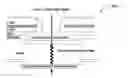
FIG. 1a depicts an example of a wafer assembly 100a having multiple n-GaN-up vertical light diode emitting (VLED) structures, where the light passes through the n-GaN to the environment outside the VLED structure, that need to be separated into individual semiconductor dies. A multilayer epitaxial structure (EPI) may be formed with an n-type GaN layer, one or more quantum wells with InGaN/GaN layers, and a p-type AlGaN/GaN layer. Although the n-type layer and the p-type layer may comprise various compound semiconductor materials, such as GaN, AlGaN, InGaN, and AlInGaN, n-GaN and p-GaN layers will be described henceforth. Various methods known to those skilled in the art may have been employed to define the distinct VLED structures.
For some VLED structures before die separation, a mirror may be disposed below the p-GaN to act as the reflector for photons. The mirror, by way of example, may be composed of multiple layers, such as Ni/Ag/Ni/Au, Ag/Ni/Au, Ti/Ag/Ni/Au, Ag/Pt or Ag/Pd or Ag/Cr, using an alloy containing Ag, Au, Cr, Pt, Pd, or Al.
One or more electrically non-conductive layers, which may also be thermally conductive layers, (hereinafter referred to as the “non-conductive material”) may have been used to fill the street, the area between the defined devices. The non-conductive material that fills the street may also cover at least a portion of the lateral surfaces of the p-GaN in an effort to further protect the multiple quantum well (MQW) active area.
A deposition of one or more metal layers may have been made on top of the mirror and the non-conductive material before the carrier substrate was removed in an effort to create one thick metal plate, for instance, labeled as “metal.” In FIG. 1a, the wafer assembly 100a has already been inverted after removal of the carrier substrate, so the metal is shown below the mirror and epitaxial structures. The one or more deposited metal layers may have been formed by electrochemical deposition (ECD) or electroless chemical deposition (ElessCD), CVD, plasma enhanced chemical vapor deposition (PECVD), physical vapor deposition (PVD), evaporation, or plasma spray. The metal layer may be single or multi-layered. In cases where the metal layer is a multi-layered structure, a plurality of metal layers with different composition (e.g., Cu, Ni, Ag, Au, Co, Cu—Co, Cu—Mo, Ni/Cu, Ni/Cu—Mo, and their alloys) may have been formed, and these layers may have been formed using different techniques. For some embodiments, the thickest metal layer may have been deposited using ECD or ElessCD, where the thickest metal layer can be any layer within the multiple layers of metal. The thickness of each metal layer may be about 10˜400 μm.
Before depositing the metal layer(s) using electrochemical or electroless chemical deposition techniques, a seed metal that is preferably electrically conductive may have been formed as seen in FIGS. 1a-c. The seed metal may be composed of copper, nickel, or tungsten that may have been deposited as one or more layers by first using evaporation, sputtering, chemical vapor deposition (CVD), or metal organic chemical vapor deposition (MOCVD) of the tungsten before using ECD to form the copper and the nickel. In the case of ECD or ElessCD for the metal layer, a deposit of conductive materials may have been made so as to form a seed metal. The seed metal may have assisted the growth of a single metal layer or of multiple metal layers via electroplating or an electroless plating process. In such cases, the seed metal may have a structure such as Ta/Cu, Ta/TaN/Cu, TaN/Cu, Ti/TaN/Cu, Ta/TiN/Cu, Ti/Cu, Ti/TiN/Cu, TiN/Cu, Cr/Au, Cr/Au/Ni/Au, Cr/Au/Ti/Ni/Au, Ti/Au, or Ti/Ni/Au.
One or more additional metal layers may have been formed above the original metal layer in an effort to protect the underlying metal layers (labeled as “Conductive oxidation/corrosion protection layer” in FIGS. 1a-c). Such additional protective metal layers may comprise, for example, Cr/Au, Ni, or Ni/Au.
After separating the carrier substrate from the epitaxial wafer assembly and, in some cases, inverting the wafer assembly as shown in FIG. 1a, the wafer assembly may be diced (i.e., dicing into individual semiconductor dies) using various steps. In these steps, methods to separate the dies include using a breaker, an air knife, or a water jet with a chemical solution (for coating the anti-oxidizing material on the cut edge of copper).
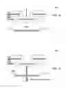
For some embodiments, a wafer assembly having dies disposed thereon may be separated by laser cut, saw cut, or water jet processes. This is represented by a downward force seen in wafer assembly 100a in FIG. 1a. After a laser has been used to cut the metal substrate, the metal may remerge together from the laser heating, as seen in wafer assembly 100b in FIG. 1b. Then, the dies may be fully separated by the application of a light force such as by using a breaker, a knife, an air knife, or a water jet, as shown regarding wafer assembly 100c in FIG. 1c.
In that the force of the breaker may be too strong and cause damage to the electrical devices, the dies may be separated by using an air knife to carefully control the dicing of the wafer, as shown regarding wafer assembly 200a in FIG. 2a.
For the case of laser cutting, it may be advantageous to protect the devices with a removable protecting coating (e.g., a polymer coating) before cutting in order to protect the devices from the debris that can be formed during the laser cutting process. It may also be advantageous to cut the devices in an oxygen-containing environment for manufacturing and junction properties.
After the laser cutting process, the devices may be cleaned in a liquid and/or a solvent in an effort to effectively remove the debris, to remove the protective coating if one is used, and to clean/passivate the junction. The liquid may be a base or an acid solution with or without an oxidizer (e.g., H2SO4:H2O2, HNO3, HNO3/HCl, NH4OH:H2O2, KOH:H2O2, and H3PO4). The solutions may be heated or may be used at room temperature. Any solvent may be used to clean the devices in an effort to remove the removable protective coating on the surface of the wafer. The solvent may be used with or without a surfactant and may be a water solution. The solvent may be used first, followed by the liquid. Alternatively, the liquid may be used first, followed by the solvent. For some embodiments, only the liquid may be used to clean the devices, or only the solvent may be used to clean the devices. It may be preferred, however, to remove the protecting coating first with the solvent, and then clean/passivate the junction with the liquid.
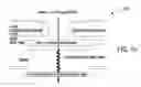
For the dicing, especially after a laser cutting operation, an anti-oxidizing passivation may be applied to the edges of the dies, such as by the use of a chemical water jet solution, as shown in FIG. 2b. The chemical solution may be, for example, a Cu, Pd, Ni, or Au plating solution.
Embodiments disclosed herein may also be applied to the fabrication of GaN-based electronic devices such as power devices, laser diodes, and vertical cavity surface emitting laser device due to its high heat dissipation rate of its metal substrate. Relative to conventional LEDs, the above teaching can improve yield, brightness, and thermal conductivity.
While the foregoing is directed to embodiments of the present invention, other and further embodiments of the invention may be devised without departing from the basic scope thereof, and the scope thereof is determined by the claims that follow.
Claims
What is claimed is:1. A method of dicing a wafer assembly comprising a plurality of semiconductor dies disposed on a metal substrate, the method comprising:
(a) applying a laser between a first and a second die to cut through at least a portion of the wafer assembly; and
(b) applying a physical force to fully separate the first die from the second die.
2. The method of claim 1, further comprising repeating step (a) for all of the plurality of semiconductor dies.
3. The method of claim 2, further comprising repeating step (b) for all of the plurality of semiconductor dies.
4. The method of claim 1, wherein the at least a portion of the wafer assembly comprises any semiconductor material between the first and second dies and at least a portion of the metal substrate.
5. The method of claim 4, wherein the at least a portion of the metal substrate remerges after applying the laser.
6. The method of claim 1, wherein applying the physical force comprises applying at least one of a breaker, a knife, an air knife, or a water jet.
7. The method of claim 6, wherein the water jet comprises only water.
8. The method of claim 1, wherein applying the physical force comprises applying a water jet with a chemical solution.
9. The method of claim 8, wherein the chemical solution is an acid or a base.
10. The method of claim 9, wherein the chemical solution comprises at least one of H2SO4:H2O2, HNO3, HNO3/HCl, NH4OH:H2O2, KOH:H2O2, or H3PO4.
11. The method of claim 8, wherein the chemical solution is at least one of a Cu, Pd, Ni, or Au plating solution.
12. The method of claim 8, wherein applying the water jet with the chemical solution leaves an anti-oxidizing passivation layer on edges of the first and second dies.
13. The method of claim 1, wherein the metal substrate comprises at least one of Cu, Ni, Au, Ag, Co, or alloys thereof.
14. The method of claim 1, wherein the metal substrate comprises a seed metal layer and a thick metal layer.
15. The method of claim 14, wherein the seed metal layer comprises at least one of Cu, Ni, W, Ta/Cu, Ta/TaN/Cu, TaN/Cu, Ti/TaN/Cu, Ta/TiN/Cu, Ti/Cu, Ti/TiN/Cu, TiN/Cu, Cr/Au, Cr/Au/Ni/Au, Ti/Au, or Ti/Ni/Au.
16. The method of claim 1, wherein the semiconductor dies are light-emitting diode (LED) dies, power device dies, laser diode dies, or vertical cavity surface emitting device dies.
17. A method of separating a plurality of vertical light-emitting diode (VLED) dies disposed on a metal substrate, the method comprising:
(a) applying a laser between adjacent VLED dies of the plurality to cut through any semiconductor material between the adjacent VLED dies and at least a portion of the metal substrate; and
(b) physically forcing the adjacent VLED dies apart.
18. The method of claim 17, wherein physically forcing the adjacent VLED dies apart comprises breaking a remerged portion of the metal substrate between the adjacent VLED dies.
19. The method of claim 17, wherein physically forcing the adjacent VLED dies apart comprises applying at least one of a breaker, a knife, an air knife, or a water jet.
20. The method of claim 17, wherein physically forcing the adjacent VLED dies apart comprises applying a water jet with a chemical solution.
21. The method of claim 20, wherein the chemical solution is at least one of a Cu, Pd, Ni, or Au plating solution.
22. The method of claim 20, wherein applying the water jet with the chemical solution leaves an anti-oxidizing passivation layer on edges of the first and second dies.
23. The method of claim 17, wherein the VLED dies comprise at least one of GaN, AlGaN, InGaN, or AlInGaN.
Images & Drawings included:
Sources:
- United States Patent and Trademark Office - verify current appl. status at the USPTO↗
Similar patent applications:
- » 20140119416
Communication system with up-converter and digital baseband processing circuit implemented in one die separated from another die having down-converter, and related communication method thereof - » 20180321307
Wafer tap domain die channel circuitry with separate die clocks - » 20210018360
Electronic packaging structure and method for manufacturing the electronic packaging structure with optical guide die separate from electronic package and photonic die - » 20230377972
DIE SEPARATION RING FOR WAFERS HAVING A LARGE DIE ASPECT RATIO - » 20180001504
Rotary cutting die for cutting corrugated board having product ejectors configured to separate die cut product without crushing flutes in the corrugated board - » 11280783
Method for eliminating backside metal peeling during die separation - » 11101028
Post singulation die separation apparatus and method for bulk feeding operation - » 10432081
Laser separated die with tapered sidewalls for improved light extraction - » 14098018
Method for reducing backside die damage during die separation process - » 10885965
Ball grid array package that includes a collapsible spacer for separating die adapter from a heat spreader
Recent applications in this class:
- » 20250056919 2025-02-13
DISPLAY DEVICE AND METHOD OF REPAIRING THE SAME - » 20250031485 2025-01-23
METHOD FOR MANUFACTURING LIGHT EMITTING DEVICE - » 20250022981 2025-01-16
APPARATUS, SYSTEM, AND METHOD FOR INCREASING CARRIER CONFINEMENT IN LIGHT-EMITTING DEVICES - » 20250015227 2025-01-09
LIGHT EMITTING DEVICE - » 20250015226 2025-01-09
METHOD OF MANUFACTURING LIGHT-EMITTING ELEMENT - » 20240429344 2024-12-26
N-POLAR III-NITRIDE NANOWIRE-BASED LED DEVICES - » 20240421247 2024-12-19
DISPLAY DEVICE USING LIGHT-EMITTING ELEMENT, AND MANUFACTURING METHOD THEREFOR - » 20240413265 2024-12-12
METHOD FOR MANUFACTURING LIGHT-EMITTING DEVICE - » 20240339560 2024-10-10
SYSTEM AND METHOD FOR REPAIRING VACANCIES RESULTING FROM MASS TRANSFER OF DEVICES - » 20240339559 2024-10-10
TRANSFERRING HEAD AND METHOD FOR MANUFACTURING ELECTRONIC DEVICE
Recent applications for this Assignee:
- » 20250143048 2025-05-01
METHOD FOR MAKING ELECTRONIC DEVICE ARRAYS USING A TEMPORARY SUBSTRATE - » 20240038958 2024-02-01
Method for making electronic device arrays using a temporary substrate - » 20230411565 2023-12-21
Light emitting diode (LED) structure having single epitaxial structure separated into light emitting zones - » 20220352449 2022-11-03
Method For Making Light Emitting Device (LED) Arrays And Electronic Products Using A Temporary Substrate And A Carrier Substrate - » 20220278261 2022-09-01
Method for making electronic device arrays using a temporary substrate and a carrier substrate - » 20210119088 2021-04-22
Single light emitting diode (LED) structure having epitaxial structure separated into light emitting zones - » 20210043820 2021-02-11
Method for making light emitting device (LED) arrays using a temporary substrate and a carrier substrate - » 20190165231 2019-05-30
Method for making light emitting device LED arrays - » 20190067529 2019-02-28
Single light emitting diode (LED) structure - » 20170018537 2017-01-19
Light emitting diode (LED) package having short circuit (VLED) die, lens support dam and same side electrodes and method of fabrication