Method of low temperature wafer bonding through Au/Ag diffusion
US20080194077A1
2008-08-14
11/808,127
2007-06-06
Abstract:
Two wafers are bonded. One wafer has a gold (Au) film on its surface; the other, a silver (Ag) film. The wafers are stuck together for a bonding process between the Au and the Ag films. Thus, an Au/Ag bonding layer is formed. The bonding layer has a high melting point and so is suitable for high-temperature processes. The bonding process also do no harm to devices on the bonded wafer.
Assignee:
- NATIONAL CENTRAL UNIVERSITY 143 🇹🇼 Taoyuan County, Taiwan
Interested in similar patents?
Get notified when new applications in this technology area are published.
Classification:
H01L21/187 » CPC main
Processes or apparatus adapted for the manufacture or treatment of semiconductor or solid state devices or of parts thereof; Manufacture or treatment of semiconductor devices or of parts thereof the devices having at least one potential-jump barrier or surface barrier, e.g. PN junction, depletion layer or carrier concentration layer the devices having semiconductor bodies comprising elements of Group IV of the Periodic System or AB compounds with or without impurities, e.g. doping materials; Joining of semiconductor bodies for junction formation by direct bonding
H01L24/03 » CPC further
Arrangements for connecting or disconnecting semiconductor or solid-state bodies; Methods or apparatus related thereto; Means for bonding being attached to, or being formed on, the surface to be connected, e.g. chip-to-package, die-attach, "first-level" interconnects; Manufacturing methods related thereto; Bonding areas ; Manufacturing methods related thereto Manufacturing methods
H01L24/05 » CPC further
Arrangements for connecting or disconnecting semiconductor or solid-state bodies; Methods or apparatus related thereto; Means for bonding being attached to, or being formed on, the surface to be connected, e.g. chip-to-package, die-attach, "first-level" interconnects; Manufacturing methods related thereto; Bonding areas ; Manufacturing methods related thereto; Structure, shape, material or disposition of the bonding areas prior to the connecting process of an individual bonding area
H01L24/08 » CPC further
Arrangements for connecting or disconnecting semiconductor or solid-state bodies; Methods or apparatus related thereto; Means for bonding being attached to, or being formed on, the surface to be connected, e.g. chip-to-package, die-attach, "first-level" interconnects; Manufacturing methods related thereto; Bonding areas ; Manufacturing methods related thereto; Structure, shape, material or disposition of the bonding areas after the connecting process of an individual bonding area
H01L24/80 » CPC further
Arrangements for connecting or disconnecting semiconductor or solid-state bodies; Methods or apparatus related thereto Methods for connecting semiconductor or other solid state bodies using means for bonding being attached to, or being formed on, the surface to be connected
H01L24/94 » CPC further
Arrangements for connecting or disconnecting semiconductor or solid-state bodies; Methods or apparatus related thereto; Batch processes at wafer-level, i.e. with connecting carried out on a wafer comprising a plurality of undiced individual devices
H01L2224/03826 » CPC further
Indexing scheme for arrangements for connecting or disconnecting semiconductor or solid-state bodies and methods related thereto as covered by; Means for bonding being attached to, or being formed on, the surface to be connected, e.g. chip-to-package, die-attach, "first-level" interconnects; Manufacturing methods related thereto; Bonding areas; Manufacturing methods related thereto; Manufacturing methods; Post-treatment of the bonding area; Applying permanent coating, e.g. in-situ coating Physical vapour deposition [PVD], e.g. evaporation, or sputtering
H01L2224/80012 » CPC further
Indexing scheme for arrangements for connecting or disconnecting semiconductor or solid-state bodies and methods related thereto as covered by; Methods for connecting semiconductor or other solid state bodies using means for bonding being attached to, or being formed on, the surface to be connected by connecting a bonding area directly to another bonding area, i.e. connectorless bonding, e.g. bumpless bonding; Pre-treatment of the bonding area; Cleaning the bonding area, e.g. oxide removal step, desmearing Mechanical cleaning, e.g. abrasion using hydro blasting, brushes, ultrasonic cleaning, dry ice blasting, gas-flow
H01L2224/8083 » CPC further
Indexing scheme for arrangements for connecting or disconnecting semiconductor or solid-state bodies and methods related thereto as covered by; Methods for connecting semiconductor or other solid state bodies using means for bonding being attached to, or being formed on, the surface to be connected by connecting a bonding area directly to another bonding area, i.e. connectorless bonding, e.g. bumpless bonding; Bonding techniques; Soldering or alloying; Diffusion bonding Solid-solid interdiffusion
H01L2924/10253 » CPC further
Indexing scheme for arrangements or methods for connecting or disconnecting semiconductor or solid-state bodies as covered by; Details of semiconductor or other solid state devices to be connected; Material of the semiconductor or solid state bodies; Semiconducting materials; Elemental semiconductors, i.e. Group IV Silicon [Si]
H01L2224/94 » CPC further
Indexing scheme for arrangements for connecting or disconnecting semiconductor or solid-state bodies and methods related thereto as covered by; Batch processes at wafer-level, i.e. with connecting carried out on a wafer comprising a plurality of undiced individual devices
H01L2224/80 » CPC further
Indexing scheme for arrangements for connecting or disconnecting semiconductor or solid-state bodies and methods related thereto as covered by Methods for connecting semiconductor or other solid state bodies using means for bonding being attached to, or being formed on, the surface to be connected
H01L21/30 IPC
Processes or apparatus adapted for the manufacture or treatment of semiconductor or solid state devices or of parts thereof; Manufacture or treatment of semiconductor devices or of parts thereof the devices having at least one potential-jump barrier or surface barrier, e.g. PN junction, depletion layer or carrier concentration layer the devices having semiconductor bodies comprising elements of Group IV of the Periodic System or AB compounds with or without impurities, e.g. doping materials Treatment of semiconductor bodies using processes or apparatus not provided for in groups -
Description
FIELD OF THE INVENTION
The present invention relates to a wafer bonding; more particularly, relates to obtaining a low temperature wafer bonding through a rapid diffusion between a gold (Au)/silver (Ag) interface to avoid a heat stress out of different coefficients of thermal expansions (CTE).
DESCRIPTION OF THE RELATED ART
Wafer bonding is a process quite often necessary in many procedures for fabricating electronic devices. And requirements for the wafer bonding include a low stress, a low temperature for the bonding process, and a high-temperature tolerance for following processes.
Traditionally, a conductive film is coated on a substrate through sputtering, where the conductive film is usually made of Au or tin (Sn). However, in fabricating a highly-integrated electronic device, an increased current density may cause a heat stress increased and a temperature heightened. In addition, the different coefficients of thermal expansions (CTE) in the Au/Sn wafer bonding interface would make the interface thin owing to a stress migration. And what is more serious is that the wafer might be broken.
In a word, the prior art does not meet the requirements of a low stress and a tolerance for high-temperature processes, where the wafer may be broken and devices on the wafer may be thus damaged. Hence, the prior art does not fulfill all users' requests on actual use.
SUMMARY OF THE INVENTION
The main purpose of the present invention is to bond wafers under aq low temperature for obtaining a bonding layer having a melting point above 900° C.
The second purpose of the present invention is to avoid heat stress on bonding multiple wafers.
The third purpose of the present invention is to prevent damages to devices on wafer owing to high-temperature processes.
To achieve the above purposes, the present invention is a method of a low temperature wafer bonding through Au/Ag diffusion, comprising steps of: (a) obtaining a first wafer; (b) coating a chromium (Cr) film, a platinum (Pt) film and a gold (Au) film on the first wafer and cleansing the first wafer; (c) obtaining a second wafer; (d coating a Cr film, a Pt film and a silver (Ag) film on the second wafer and cleansing the second wafer; and (e) sticking the first and the second wafers together and putting the first and the second wafers into a furnace to be bonded through an Au/Ag diffusion under a low temperature to obtain an Au/Ag bonding layer having a melting point above 900° C. Accordingly, a novel method of a low temperature wafer bonding through Au/Ag diffusion is obtained.
BRIEF DESCRIPTIONS OF THE DRAWINGS
The present invention will be better understood from the following detailed description of the preferred embodiment according to the present invention, taken in conjunction with the accompanying drawings, in which
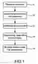
FIG. 1 is the flow view showing the preferred embodiment according to the present invention;
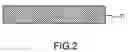
FIG. 2 is the structural view showing the first wafer;
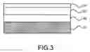
FIG. 3 is the structural view showing the first wafer coated with a Cr film, a Pt film and an Au film;
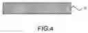
FIG. 4 is the structural view showing the second wafer;
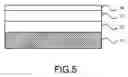
FIG. 5 is the structural view showing the second wafer coated with a Cr film, a Pt film and an Ag film; and
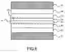
FIG. 6 is the structural view showing the preferred embodiment.
DESCRIPTION OF THE PREFERRED EMBODIMENT
The following description of the preferred embodiment is provided to understand the features and the structures of the present invention.
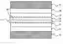
Please refer to FIG. 1 to FIG. 6, which are a flow view showing a preferred embodiment according to the present invention; structural views showing a first wafer and the first wafer coated with a Cr film, a Pt film and an Au film; structural views showing a second wafer and the second wafer coated with a Cr film, a Pt film and an Ag film; and a structural view showing the preferred embodiment. As shown in the figures, the present invention is a method of a low temperature wafer bonding through Au/Ag diffusion, comprising the following step:
(a) Obtaining a first wafer [11]: As shown in FIG. 2, a first wafer [21] is obtained, where the first wafer [21] is a silicon (Si) wafer.
(b) Evaporating metal films and processing a cleansing [12]: As shown In FIG. 3, an electron-gun (E-gun) evaporator with a current between 50 and 250 milli-ampere (mA) is used to sequentially coat a chromium (Cr) film [22], a platinum (Pt) film [23] and a gold (Au) film [24] on the first wafer [21]. Then the first wafer [21] with the coated films are put into a solution having acetone and isopropanol to be cleansed with an ultra-sonic shaker; and then is washed with a de-ionized water and hot-dried with nitrogen (N2).
(c) Obtaining a second wafer [13]: As shown in FIG. 4, a second wafer [31] is obtained, where the second wafer [31] is a Si wafer.
(d) Evaporating metal films and processing a cleansing [14]: As shown in FIG. 5, the E-gun evaporator with a current between 50 and 250 mA is used to sequentially coat a Cr film [32], a Pt film [33] and a silver (Ag) film [34] on the second wafer [31]. Then the second wafer [31] having the coated films are put into the solution having acetone and isopropanol to be cleansed with the ultra-sonic shaker; and then is washed with the de-ionized water and hot-dried with nitrogen (N2).
(e) Bonding the wafers under a low temperature [15]: As shown in FIG. 6, the first wafer [21] having the Au film [24] and the second wafer [31] having the Ag film [34] are then stuck together and are put into a furnace to bond the Au film [24] of the first wafer [21] and the Ag film [34] of the second wafer [31] for obtaining an Au/Ag bonding layer [41] through a diffusion between the Au film and the Ag film under a pressure between 10−2 and 10−6 torr and a temperature between 100 and 300 Celsius degrees (° C.), where the Au/Ag bonding layer [41] has a melting point above 900° C.
Thus, a novel method of a low temperature wafer bonding through Au/Ag diffusion is obtained.
Consequently, a low temperature wafer bonding is achieved through a rapid diffusion between an Au/Ag interface 411, where a low stress, a low temperature for a bonding process and a high-temperature tolerance for following processes are obtained. Besides, a heat stress is avoid, where the heat stress may be originally obtained owing to different coefficients of thermal expansion (CTE) for different materials on bonding different wafers. Furthermore, the non-porous wafer bonding interface obtained is good for the high-temperature processes that follows; and causes no damage to devices on the bonded wafer.
To sum up, the present invention is a method of a low temperature wafer bonding through Au/Ag diffusion, where a temperature for wafer bonding is reduced owing to a rapid diffusion between an Au/Ag interface; a low stress, a low temperature for a bond in g process and a high-temperature tolerance for following processes is obtained; and a heat stress is avoid, which may be originally obtained owing to different CTE coefficients for different materials on bonding different wafers.
The preferred embodiment herein disclosed is not intended to unnecessarily limit the scope of the invention. Therefore, simple modifications or variations belonging to the equivalent of the scope of the claims and the instructions disclosed herein for a patent are all within the scope of the present invention.
Claims
What is claimed is:1. A method of a low temperature wafer bonding through Au/Ag diffusion, comprising steps of:
(a) obtaining a first wafer;
(b) evaporating metal films having a most exterior film of gold (Au) on said first wafer and processing a cleansing;
(c) obtaining a second wafer;
(d) evaporating metal films having a most exterior film of silver (Ag) on said second wafer and processing a cleansing; and
(e) connecting said first wafer and said second wafer and putting said first wafer and said second wafer into a furnace to be bonded under a temperature to obtain an Au/Ag bonding layer through an Au/Ag diffusion.
2. The method according to claim 1, wherein each film of said metal films is variously selected from a group consisting of a chromium (Cr) film, a platinum (Pt) film, an Au film and an Ag film.
3. The method according to claim 1, wherein said cleansing is processed with an ultra-sonic shaker.
4. The method according to claim 1, wherein said temperature in step (e) is located between 100 and 300 Celsius degrees.
5. The method according to claim 1, wherein said bonding is processed for a period between 30 minutes and 4 hours.
6. The method according to claim 1, wherein said furnace has a pressure between 10−2 and 10−6 torr.
7. The method according to claim 1, wherein said first wafer and said second wafer are silicon wafers.
Images & Drawings included:
Sources:
- United States Patent and Trademark Office - verify current appl. status at the USPTO↗
Recent applications in this class:
- » 20240371641 2024-11-07
METHOD OF MANUFACTURING COMPOUND SEMICONDUCTOR BONDED SUBSTRATE AND COMPOUND SEMICONDUCTOR BONDED SUBSTRATE - » 20240266172 2024-08-08
SEMICONDUCTOR STRUCTURE COMPRISING AN ELECTRICALLY CONDUCTIVE BONDING INTERFACE, AND ASSOCIATED MANUFACTURING METHOD - » 20240128085 2024-04-18
Carrier-Assisted Method for Parting Crystalline Material Along Laser Damage Region - » 20240063022 2024-02-22
WAFER BONDING PROCESS WITH REDUCED OVERLAY DISTORTION - » 20240038536 2024-02-01
PLASMA PROCESSING APPARATUS, WAFER TO WAFER BONDING SYSTEM AND WAFER TO WAFER BONDING METHOD - » 20240030033 2024-01-25
METHOD FOR PRODUCING A SEMICONDUCTOR STRUCTURE COMPRISING AN INTERFACE REGION INCLUDING AGGLOMERATES - » 20230326757 2023-10-12
SUBSTRATE PROCESSING METHOD AND SUBSTRATE PROCESSING APPARATUS - » 20230307234 2023-09-28
SEMICONDUCTOR DEVICE WITH TWO-DIMENSIONAL MATERIALS - » 20230223264 2023-07-13
METHOD FOR MANUFACTURING SEMICONDUCTOR STRUCTURE AND SEMICONDUCTOR STRUCTURE - » 20230197453 2023-06-22
STRUCTURE WITH CONDUCTIVE FEATURE FOR DIRECT BONDING AND METHOD OF FORMING SAME
Recent applications for this Assignee:
- » 20180041566 2018-02-08
Description files and web service protocols for tasking capability on internet of things - » 20160292894 2016-10-06
Diagram building system and method for a signal data decomposition and analysis - » 20160230264 2016-08-11
Application of metallic glass coating for improving fatigue resistance of aluminum alloys - » 20160081561 2016-03-24
Noninvasive arterial condition detecting method, system, and non-transitory computer readable storage medium - » 20160007689 2016-01-14
Button device - » 20150280849 2015-10-01
Non-coherent neighbor cell searching method - » 20150259302 2015-09-17
Indication of naphtho[2,3-F]quinoxaline-7,12-dione compound in alleviating pain - » 20150258073 2015-09-17
Indication of anthra[2,1,c][1,2,5]thiadiazole-6,11-dione compound in alleviating pain - » 20150243838 2015-08-27
Light-emitting diode structure having progressive work function layer - » 20150093828 2015-04-02
Method for manufacturing a cell culturing article