Method for connecting a precious metal surface to a polymer
US20100307804A1
2010-12-09
12/742,179
2008-11-14
✅ Patent granted
US 9,254,993 B2
2016-02-09
WO; PCT/EP2008/009829; 20081114
WO; WO2009/062753; 20090522
Dah-Wei D Yuan | Jose Hernandez-Diaz
Schwegman Lundberg & Woessner, P.A.
2031-08-03
Abstract:
The invention relates to a method for connecting a precious metal surface to a polymer, wherein a layer made of 20% to 40% gold and 80% to 60% silver is deposited on a substrate and the silver is subsequently selectively removed in order to produce a nanoporous gold layer. A fluid polymer is applied to the gold layer and cured.
Assignee:
Applicant:
Interested in similar patents?
Get notified when new applications in this technology area are published.
Classification:
H05K1/00 IPC
Printed circuits
H05K1/00 IPC
Printed circuits
B05D3/00 IPC
Pretreatment of surfaces to which liquids or other fluent materials are to be applied; After-treatment of applied coatings, e.g. intermediate treating of an applied coating preparatory to subsequent applications of liquids or other fluent materials
B05D5/12 IPC
Processes for applying liquids or other fluent materials to surfaces to obtain special surface effects, finishes or structures to obtain a coating with specific electrical properties
B05D5/00 IPC
Processes for applying liquids or other fluent materials to surfaces to obtain special surface effects, finishes or structures
B05D1/32 IPC
Processes for applying liquids or other fluent materials using means for protecting parts of a surface not to be coated, e.g. using stencils, resists
B05D3/02 IPC
Pretreatment of surfaces to which liquids or other fluent materials are to be applied; After-treatment of applied coatings, e.g. intermediate treating of an applied coating preparatory to subsequent applications of liquids or other fluent materials by baking
B05D3/10 IPC
Pretreatment of surfaces to which liquids or other fluent materials are to be applied; After-treatment of applied coatings, e.g. intermediate treating of an applied coating preparatory to subsequent applications of liquids or other fluent materials by other chemical means
H01L21/441 IPC
Processes or apparatus adapted for the manufacture or treatment of semiconductor or solid state devices or of parts thereof; Manufacture or treatment of semiconductor devices or of parts thereof the devices having at least one potential-jump barrier or surface barrier, e.g. PN junction, depletion layer or carrier concentration layer the devices having semiconductor bodies not provided for in groups, , , and with or without impurities, e.g. doping materials; Manufacture of electrodes on semiconductor bodies using processes or apparatus not provided for in groups - Deposition of conductive or insulating materials for electrodes
C23C14/34 IPC
Coating by vacuum evaporation, by sputtering or by ion implantation of the coating forming material characterised by the process of coating Sputtering
C25D5/48 IPC
Electroplating characterised by the process; Pretreatment or after-treatment of workpieces After-treatment of electroplated surfaces
C25D5/54 IPC
Electroplating characterised by the process; Pretreatment or after-treatment of workpieces Electroplating of non-metallic surfaces
B81B7/0006 » CPC main
Microstructural systems; Auxiliary parts of microstructural devices or systems Interconnects
H01L2924/09701 » CPC further
Indexing scheme for arrangements or methods for connecting or disconnecting semiconductor or solid-state bodies as covered by with a principal constituent of the material being a combination of two or more materials provided in the groups - ; Glass-ceramics, e.g. devitrified glass Low temperature co-fired ceramic [LTCC]
H01L23/00 IPC
Details of semiconductor or other solid state devices
H01L24/28 » CPC further
Arrangements for connecting or disconnecting semiconductor or solid-state bodies; Methods or apparatus related thereto; Means for bonding being attached to, or being formed on, the surface to be connected, e.g. chip-to-package, die-attach, "first-level" interconnects; Manufacturing methods related thereto; Layer connectors, e.g. plate connectors, solder or adhesive layers; Manufacturing methods related thereto Structure, shape, material or disposition of the layer connectors prior to the connecting process
H05K3/383 » CPC further
Apparatus or processes for manufacturing printed circuits; Improvement of the adhesion between the insulating substrate and the metal by special treatment of the metal by microetching
H05K3/383 » CPC further
Apparatus or processes for manufacturing printed circuits; Improvement of the adhesion between the insulating substrate and the metal by special treatment of the metal by microetching
H05K2201/0116 » CPC further
Indexing scheme relating to printed circuits covered by; Dielectrics; Properties and characteristics in general Porous, e.g. foam
H05K2201/0116 » CPC further
Indexing scheme relating to printed circuits covered by; Dielectrics; Properties and characteristics in general Porous, e.g. foam
C22C1/08 » CPC further
Making alloys Alloys with open or closed pores
H05K3/38 IPC
Apparatus or processes for manufacturing printed circuits Improvement of the adhesion between the insulating substrate and the metal
H05K3/38 IPC
Apparatus or processes for manufacturing printed circuits Improvement of the adhesion between the insulating substrate and the metal
H01L2924/01004 » CPC further
Indexing scheme for arrangements or methods for connecting or disconnecting semiconductor or solid-state bodies as covered by; Chemical elements Beryllium [Be]
H01L2924/01005 » CPC further
Indexing scheme for arrangements or methods for connecting or disconnecting semiconductor or solid-state bodies as covered by; Chemical elements Boron [B]
H01L2924/01015 » CPC further
Indexing scheme for arrangements or methods for connecting or disconnecting semiconductor or solid-state bodies as covered by; Chemical elements Phosphorus [P]
H01L2924/01024 » CPC further
Indexing scheme for arrangements or methods for connecting or disconnecting semiconductor or solid-state bodies as covered by; Chemical elements Chromium [Cr]
H01L2924/01029 » CPC further
Indexing scheme for arrangements or methods for connecting or disconnecting semiconductor or solid-state bodies as covered by; Chemical elements Copper [Cu]
H01L2924/0132 » CPC further
Indexing scheme for arrangements or methods for connecting or disconnecting semiconductor or solid-state bodies as covered by; Alloys Binary Alloys
H01L2924/01032 » CPC further
Indexing scheme for arrangements or methods for connecting or disconnecting semiconductor or solid-state bodies as covered by; Chemical elements Germanium [Ge]
H01L2924/01033 » CPC further
Indexing scheme for arrangements or methods for connecting or disconnecting semiconductor or solid-state bodies as covered by; Chemical elements Arsenic [As]
H01L2924/01047 » CPC further
Indexing scheme for arrangements or methods for connecting or disconnecting semiconductor or solid-state bodies as covered by; Chemical elements Silver [Ag]
H01L2924/01074 » CPC further
Indexing scheme for arrangements or methods for connecting or disconnecting semiconductor or solid-state bodies as covered by; Chemical elements Tungsten [W]
H01L2924/01078 » CPC further
Indexing scheme for arrangements or methods for connecting or disconnecting semiconductor or solid-state bodies as covered by; Chemical elements Platinum [Pt]
H01L2924/01079 » CPC further
Indexing scheme for arrangements or methods for connecting or disconnecting semiconductor or solid-state bodies as covered by; Chemical elements Gold [Au]
H01L2924/01082 » CPC further
Indexing scheme for arrangements or methods for connecting or disconnecting semiconductor or solid-state bodies as covered by; Chemical elements Lead [Pb]
H05K2203/0361 » CPC further
Indexing scheme relating to apparatus or processes for manufacturing printed circuits covered by; Metal processing Stripping a part of an upper metal layer to expose a lower metal layer, e.g. by etching or using a laser
H05K2203/0361 » CPC further
Indexing scheme relating to apparatus or processes for manufacturing printed circuits covered by; Metal processing Stripping a part of an upper metal layer to expose a lower metal layer, e.g. by etching or using a laser
B81B7/00 IPC
Microstructural systems; Auxiliary parts of microstructural devices or systems
H05K3/00 IPC
Apparatus or processes for manufacturing printed circuits
H05K3/00 IPC
Apparatus or processes for manufacturing printed circuits
C22C1/02 » CPC further
Making alloys by melting
H05K3/24 » CPC further
Apparatus or processes for manufacturing printed circuits; Secondary treatment of printed circuits Reinforcing the conductive pattern
H05K3/24 » CPC further
Apparatus or processes for manufacturing printed circuits; Secondary treatment of printed circuits Reinforcing the conductive pattern
H05K3/28 » CPC further
Apparatus or processes for manufacturing printed circuits; Secondary treatment of printed circuits Applying non-metallic protective coatings
H05K3/28 » CPC further
Apparatus or processes for manufacturing printed circuits; Secondary treatment of printed circuits Applying non-metallic protective coatings
Description
The invention relates to a method for connecting a precious metal surface to a polymer and also to a layer composite produced therewith, comprising a porous precious metal layer and a polymer layer which has at least partially penetrated therein, in particular for applications on microelectronic and micromechanical semiconductor wafers and an microoptical applications and also for circuit substrates with organic layers.
In semiconductor technology there is a large number of cases in which a polymer is intended to be applied on a precious metal layer, for example a gold layer. One example is rewiring layers for changing the connection arrangement on an electronic semiconductor, comprising at least one organic dielectric layer and at least one metallic wiring layer. A further example is high frequency-suitable circuit substrates which are constructed from a layer composite of e.g. gold and an organic dielectric, such as for example polyimide, PBO, BCB or an epoxide. In another case, for example solder stop lacquers which are applied on gold-coated strip conductors, are used in order to delimit the wetting of the strip conductor by melted solder. In a further case, metal-polymer layers are used to produce stacks of semiconductor components and the electrical contacting thereof. The adhesion of polymer layers on precious metals, such as gold, is however critical. In the case of mechanical or thermomechanical stressing of the layer composite, the result, because of the low adhesion, is separation between the polymer and the precious metal layer. It has been attempted in the state of the art to increase the surface by roughening the latter and hence to improve the adhesion, or adhesives, e.g. Titan, have been used in order to improve the specific adhesion. The results are however either unsatisfactory or very complex to achieve.
The object underlying the invention is to produce a method and a surface structure with which the adhesive strength of polymer layers on gold surfaces is improved for semiconductor materials and circuit substrates in microelectronic, micromechanical or microoptical applications.
This object is achieved according to the invention by the features of the main claim.
As a result of the fact that the surface to be provided with polymer is formed by a sponge-like nanoporous gold layer which is achieved by deposition of a layer made of 20% to 40% gold and 80% to 60% silver onto a substrate and subsequent selective removal of the silver in order to produce the nanoporous gold layer, that the liquid polymer is applied on this sponge structure and is cured, very high adhesive strength of the polymer layer on the gold layer is achieved since the applied liquid polymer penetrates into the sponge-like structures and forms a three-dimensional interface with mechanical interlocking between the materials.
Advantageous developments and improvements are possible as a result of the measures indicated in the sub-claims.
Advantageously, a substrate used in electronics, microelectronics, micromechanics and/or microoptics is chosen as substrate, which substrate can be provided with electrically conducting, in particular structured metallisations. It can be a semiconductor wafer or a semiconductor chip produced therefrom or a single or multilayer circuit substrate.
The nanoporous gold layer can be applied on an already present metallic layer which can be the metallisation of the substrate, in particular a layer formed from gold.
The nanoporous gold layer can be deposited on wafers with microelectronic circuits or micromechanical elements or on a circuit substrate material, in particular on organic laminates, thin-film ceramics or thin-film glass.
The nanoporous gold layer or the combination of nanoporous gold layer and metallisation can be deposited on semiconductor materials in order to produce a rewiring structure or on a circuit substrate in order to produce a multilayer circuit.
The nanoporous gold layer or the combination of nanoporous gold layer and metallisation can serve to produce a stack arrangement comprising a plurality of microelectronic circuits or micromechanical or microoptical elements on a semiconductor base.
In the method according to the invention, the Ag/Au layer used in the intermediate step can be produced simply in a known deposition process, electrochemical deposition, deposition by means of electron beam evaporation or sputtering being able to be chosen. Advantageously, these can be in particular the electrochemical or galvanic process since the material consumption can be less and hence cost savings can be made. Also the silver can be removed by normal processes, for example by reverse electrolysis of the galvanic deposition process or by free etching.
The nanoporous sponge-like gold layer with a high continuous pore proportion and high freely accessible surface can be produced on any substrates. By varying the composition of the gold and of the silver, the density of the nanoporous gold layer can be varied.
Advantageously, the sponge-like gold layer can be pre-treated in its surface, for example by reactive ion etching or hydrophilising, in order to improve the wetting.
Corresponding to the purposes of use, the nanoporous gold layer can be structured.
By providing a tempering process after production of the nanoporous gold layer, the size of its pores can be adjusted.
Advantageously, the deposition process of the Ag/Au layer can be improved by advance application of a plating base or an adhesive layer.
It is particularly advantageous that a vacuum is applied before, during or after application of the polymer in order to move the air out of the pores and to achieve deep penetration of the polymer into the sponge-like structure.
The polymer layer can be structured according to the configuration. Thus it can be expedient if the polymer remains merely where a porous surface is present.
The method according to the invention can be used in microsystem technology for the production of dielectric layers or as solder stop lacquer on gold-coated strip conductors or the like. The polymer can be configured also as a passivation layer on a wafer and, after separation, on a chip.
With the method according to the invention, a microelectronic, micromechanical or microoptical component with at least one precious metal surface connected to a polymer can be produced, the precious metal surface as gold layer being nanoporous and sponge-like and the polymer layer having penetrated at least partially into the sponge structure.
A circuit substrate made of organic material, ceramic or glass with at least one precious metal surface connected to a polymer can also be produced, the precious metal surface as gold layer being nanoporous and sponge-like and the polymer layer having penetrated at least partially into the sponge structure.
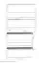
The method according to the invention is explained in more detail in the subsequent description using the accompanying drawing.
The single FIGURE shows schematically the layer construction with various steps of the method according to the invention for producing the nanoporous gold layer and subsequent application of the polymer.
Production of a nanoporous gold layer is described with reference to the FIGURE. First of all, corresponding to FIG. 1a, a plating base 2 in the form of a layer for adhesion strengthening, for example made of titanium, titanium/tungsten or chromium, is applied on the substrate and, thereupon, a starter layer made of gold, nickel, copper or platinum, this being able to take place by sputtering.
As further essential step corresponding to FIG. 1b, a galvanic deposition of a gold/silver alloy is undertaken, the alloy-forming metallic elements being present firstly in an electrolyte and the electrochemical deposition from the electrolyte takes place by applying a voltage. The composition of the gold/silver deposition is thereby in the range of 20% to 40% gold and 80% to 60% silver. As intermediate step corresponding to FIG. 1b, a gold/silver layer 3 is therefore situated on the starter layer 2.
Between FIG. 1b and the representation according to FIG. 1c in which a nanoporous gold layer 4 merging into the starter gold layer 2 is represented, the dissolving of the silver out of the layer 3 takes place, this selective dissolving or dealloying being able to be implemented in different ways. One possibility, in particular if electrochemical deposition is used, is reverse electrolysis of the principle of galvanic deposition in a suitable electrolyte, in which a voltage is applied to the electrodes, by means of which the silver is dissolved out but the gold is not affected. Another possibility is selective dealloying by external currentless etching of the silver, e.g. in nitric acid-containing solutions.
In the process for dissolving out the silver, a surface reaction takes place in the Ag/Au layer 3, during which reaction silver from the uppermost metal layer goes into solution as ion. The remaining Au atoms accumulate on the surface to form islands and protect the surface there selectively from further dissolution. Subsequently, silver is dissolved out of the next metal layer which is not covered by a gold island. By means of repeated accumulation of the moveable Au atoms from the layer, a 3D sponge layer with nanoscale pores grows slowly. The sponge-like nanoporous layer is designated in FIG. 1c with 4.
The deposition of the Ag/Au layer 3 was described further back as the electrochemical process, however it can also be produced by vapour deposition, e.g. electron beam evaporation or sputtering. Similarly to FIG. 1a, an adhesive layer with materials generally used in thin-film technology is applied in advance. In the case of sputtering or cathodic sputtering, the silver and the gold can be sputtered alternately or in parallel, the multilayers diffusing one into the other by tempering.
In the description according to FIG. 1, only the main steps for producing the nanoporous gold layer 4 have been explained. Of course, further method steps can be interposed. Thus, between the representations of FIGS. 1a and 1b, for example a photosensitive lacquer is applied and, corresponding to the specifications of the layer configuration, is structured lithographically. The thus produced lacquer mask can be removed again, according to the method course, before and after the selective dealloying of the silver. If the plating base 2 is intended to be etched away, a second lacquer mask is structured for protection of the nanoporous layer 4 and subsequently the plating base is etched. After removing this second lacquer mask, possibly further structurings of the nanoporous or sponge-like gold layer 4 can be undertaken.
Between the layer construction according to FIG. 1c and according to that of FIG. 1d which shows a polymer layer 5 on and in the sponge-like nanoporous gold layer 4, the surface of the sponge-like gold layer 4 is pre-treated, e.g. by reactive ion etching or by hydrophilising in order to improve wetting and a liquid polymer is applied, which is for example a benzocyclobutene prepolymer or a polyimide. In order that the liquid polymer penetrates better into the sponge-like structure, the arrangement is placed under vacuum, as a result of which penetration of the liquid polymer into the pores is assisted.
If a photosensitive polymer layer 5 is intended to be structured, it is exposed with a mask and developed. Finally, the polymer layer is polymerised, crosslinked and cured.
Claims
What is claimed is:1. A method for connecting a precious metal surface to a polymer, the method comprising:
depositing a layer made of 20% to 40% gold and 80% to 60% silver onto a substrate,
selectively removing the silver in order to achieve a nanoporous gold layer,
applying a liquid polymer, and
curing of the polymer.
2. The method according to claim 1, wherein a substrate used in electronics, microelectronics, micromechanics and/or microoptics is chosen as the substrate.
3. The method according to claim 2, wherein the substrate is provided with structured electrical conductors and is a semiconductor wafer or a semiconductor chip produced therefrom and/or a single or multilayer circuit substrate.
4. The method according to claim 1, wherein the nanoporous gold layer is applied on an already present metallic layer formed using gold.
5. The method according to claim 1, comprising depositing the nanoporous gold layer on a wafer with a microelectronic circuit or a micromechanical element and/or on a circuit substrate material that includes an organic laminate, a ceramic and/or a glass material.
6. The method according to claim 1, comprising depositing the nanoporous gold layer on a semiconductor material to produce a rewiring structure and/or on a circuit substrate in order to produce a multilayer circuit.
7. The method according to claim 1, comprising forming the nanoporous gold layer to produce a stack arrangement comprising a plurality of microelectronic circuits and/or micromechanical and/or microoptical elements on a semiconductor base.
8. The method according to claim 1, comprising forming the polymer from BCB, polyimide, PBO and/or an epoxide.
9. The method according to claim 1, wherein the deposition of the layer made of gold and silver includes a galvanic and/or electrochemical route.
10. The method according to claim 1, wherein the deposition of the layer made of gold and silver includes vapour deposition and/or sputtering.
11. The method according to claim 1, wherein, before the deposition of the layer made of gold and silver, a plating base with adhesion strengthening is applied on the substrate.
12. The method according to claim 10, comprising applying an adhesive layer.
13. The method according to claim 1, wherein before the deposition of the layer made of gold and silver, a lithographically structured plating base or adhesive layer is applied on the substrate.
14. The method according to claim 1, wherein the selective removal of the silver includes reverse electrolysis of the galvanic deposition.
15. The method according to claim 1, wherein the selective removal of the silver includes etching of the silver.
16. The method according to claim 1, comprising, before or after the removal of the silver, removing a lacquer mask used for structuring the layer made of gold and silver to be deposited.
17. The method according to claim 16, wherein a galvanic starter layer is firstly removed after applying the gold-silver layer and removing the lacquer mask, the silver is dealloyed and an adhesive layer is removed, without requiring masking of the nanoporous gold using a second lacquer mask in a suitable aqueous solution.
18. The method according to claim 1, comprising tempering the nanoporous gold layer to adjust the pore size.
19. The method according to claim 1, comprising structuring the nanoporous gold layer.
20. The method according to claim 1, comprising pre-treating the nanoporous gold layer to provide better wetting, including reactive ion etching, and/or hydrophilising.
21. The method according to claim 1, comprising applying the polymer in liquid form.
22. The method according to claim 1, comprising vapor depositing the polymer.
23. The method according to claim 1, comprising placing the polymer in liquid state under vacuum to provide better penetration into the nanoporous gold layer.
24. The method according to claim 1, comprising structuring the polymer layer.
25. The method according to claim 1, comprising polymerizing and crosslinking the polymer layer after application and penetration into the nanoporous gold layer.
26. The method according to claim 1, comprising configuring the polymer as an organic dielectric.
27. The method according to claim 1, comprising configuring the polymer as a solder-stop lacquer.
28. The method according to claim 1, wherein the polymer is configured as a passivation layer on a wafer and, after separation, on a chip.
29. A microelectronic, micromechanical and/or microoptical component with at least one precious metal surface connected to a polymer, the precious metal surface being nanoporous and sponge-like and the polymer layer having penetrated at least partially into the sponge structure.
30. A circuit substrate made of organic material, ceramic and/or glass with at least one precious metal surface connected to a polymer, the precious metal surface being nanoporous and sponge-like and the polymer layer having penetrated at least partially into the sponge structure.
Images & Drawings included:
Sources:
- United States Patent and Trademark Office - verify current appl. status at the USPTO↗
Recent applications in this class:
- » 20250250160 2025-08-07
ACTUATOR DEVICE - » 20250243051 2025-07-31
BYPASS STRUCTURE - » 20250136435 2025-05-01
STRETCHABLE ELECTRICAL INTERCONNECT, FLEXIBLE ELECTRONIC SYSTEM, AND FABRICATION METHOD THEREOF - » 20250059023 2025-02-20
FOUNDRY-COMPATIBLE THROUGH SILICON VIA PROCESS FOR INTEGRATED MICRO-SPEAKER AND MICROPHONE - » 20250011160 2025-01-09
METHOD FOR FABRICATING A MICROELECTRONICS H-FRAME DEVICE - » 20250002329 2025-01-02
MEMS SENSOR - » 20240317577 2024-09-26
MEMS ELEMENT, OPTICAL SCANNING DEVICE, AND DISTANCE MEASURING DEVICE - » 20240270566 2024-08-15
ELECTRONIC DEVICE AND METHOD OF FABRICATING THE SAME - » 20240190699 2024-06-13
Actuator device - » 20240101413 2024-03-28
SELF-ALIGNED AIR GAP FORMATION IN MICROELECTRONICS PACKAGES
Recent applications for this Assignee:
- » 20210384955 2021-12-09
Methods and apparatuses for providing antenna port related information in a communications network - » 20140291308 2014-10-02
Device, arrangement, and method for the interference structuring of planar samples - » 20130203065 2013-08-08
Method for electrochemical detection of binding reactions - » 20130186852 2013-07-25
Device and method for producing targeted flow and current density patterns in a chemical and/or electrolytic surface treatment - » 20100295928 2010-11-25
Method and device for the autostereoscopic representation of image information - » 20050014254 2005-01-20
Isolated adult pluripotent stem cells and methods for isolating and cultivating thereof - » 10469935 2008-11-04
Coating powder of Cr or V doped titanium suboxides - » 9508042 2007-10-02
Method for detecting time dependent modes of dynamic systems