Method of manufacturing substrate for flip chip and substrate for flip chip manufactured using the same
US20110079926A1
2011-04-07
12/923,621
2010-09-29
✅ Patent granted
US 8,486,760 B2
2013-07-16
-
-
S. V. Clark | Krista Soderholm
2031-08-05
Abstract:
There is provided a method of manufacturing a substrate for flip chip, and a substrate for flip chip manufactured using the same. The method includes providing a base substrate including at least one conductive pad, forming a solder resist layer on the base substrate, the solder resist layer including a first opening exposing the conductive pad, forming a dry film on the solder resist layer, the dry film including a second opening connected with the first opening, forming a metal post in the first opening and a part of the second opening, filling the second opening above the metal post with solder paste, forming a solder cap by performing a reflow process on the filled solder paste, planarizing a surface of the solder cap, and removing the dry film. Accordingly, fine pitches and improve reliability can be achieved.
Inventors:
- Hueng Jae Oh 5 🇰🇷 Gyunggi-do, South Korea
- Jin Won Choi 13 🇰🇷 Gyunggi-do, South Korea
- Dong Gyu Lee 7 🇰🇷 Suwon, South Korea
- Tae Joon Chung 13 🇰🇷 Seoul, South Korea
- Seon Jae Mun 5 🇰🇷 Suwon, South Korea
- Jin Won Choi 12 🇰🇷 Yongin, South Korea
- Dong Gyu LEE 5 🇰🇷 Gyunggi-do, South Korea
- Seon Jae MUN 6 🇰🇷 Gyunggi-do, South Korea
- Hueng Jae OH 5 🇰🇷 Suwon, South Korea
Assignee:
- SAMSUNG ELECTRO-MECHANICS CO., LTD. 3,010 🇰🇷 Suwon, South Korea
Applicant:
Interested in similar patents?
Get notified when new applications in this technology area are published.
Classification:
H05K3/4007 » CPC main
Apparatus or processes for manufacturing printed circuits; Forming printed elements for providing electric connections to or between printed circuits Surface contacts, e.g. bumps
H05K3/4007 » CPC main
Apparatus or processes for manufacturing printed circuits; Forming printed elements for providing electric connections to or between printed circuits Surface contacts, e.g. bumps
H01L21/4853 » CPC further
Processes or apparatus adapted for the manufacture or treatment of semiconductor or solid state devices or of parts thereof; Manufacture or treatment of semiconductor devices or of parts thereof the devices having at least one potential-jump barrier or surface barrier, e.g. PN junction, depletion layer or carrier concentration layer; Manufacture or treatment of parts, e.g. containers, prior to assembly of the devices, using processes not provided for in a single one of the subgroups -; Conductive parts; Leads on or in insulating or insulated substrates, e.g. metallisation Connection or disconnection of other leads to or from a metallisation, e.g. pins, wires, bumps
H01L23/49816 » CPC further
Details of semiconductor or other solid state devices; Arrangements for conducting electric current to or from the solid state body in operation, e.g. leads, terminal arrangements ; Selection of materials therefor consisting of soldered constructions; Leads, on insulating substrates,; Additional leads joined to the metallisation on the insulating substrate, e.g. pins, bumps, wires, flat leads Spherical bumps on the substrate for external connection, e.g. ball grid arrays [BGA]
H01L24/81 » CPC further
Arrangements for connecting or disconnecting semiconductor or solid-state bodies; Methods or apparatus related thereto; Methods for connecting semiconductor or other solid state bodies using means for bonding being attached to, or being formed on, the surface to be connected using a bump connector
H05K3/3485 » CPC further
Apparatus or processes for manufacturing printed circuits; Assembling printed circuits with electric components, e.g. with resistor electrically connecting electric components or wires to printed circuits by soldering; Solder materials or compositions; Methods of application thereof Applying solder paste, slurry or powder
H01L24/05 » CPC further
Arrangements for connecting or disconnecting semiconductor or solid-state bodies; Methods or apparatus related thereto; Means for bonding being attached to, or being formed on, the surface to be connected, e.g. chip-to-package, die-attach, "first-level" interconnects; Manufacturing methods related thereto; Bonding areas ; Manufacturing methods related thereto; Structure, shape, material or disposition of the bonding areas prior to the connecting process of an individual bonding area
H01L24/11 » CPC further
Arrangements for connecting or disconnecting semiconductor or solid-state bodies; Methods or apparatus related thereto; Means for bonding being attached to, or being formed on, the surface to be connected, e.g. chip-to-package, die-attach, "first-level" interconnects; Manufacturing methods related thereto; Bump connectors ; Manufacturing methods related thereto Manufacturing methods
H01L2224/03912 » CPC further
Indexing scheme for arrangements for connecting or disconnecting semiconductor or solid-state bodies and methods related thereto as covered by; Means for bonding being attached to, or being formed on, the surface to be connected, e.g. chip-to-package, die-attach, "first-level" interconnects; Manufacturing methods related thereto; Bonding areas; Manufacturing methods related thereto; Manufacturing methods; Methods of manufacturing bonding areas involving a specific sequence of method steps the bump being used as a mask for patterning the bonding area
H01L2224/0401 » CPC further
Indexing scheme for arrangements for connecting or disconnecting semiconductor or solid-state bodies and methods related thereto as covered by; Means for bonding being attached to, or being formed on, the surface to be connected, e.g. chip-to-package, die-attach, "first-level" interconnects; Manufacturing methods related thereto; Bonding areas; Manufacturing methods related thereto; Structure, shape, material or disposition of the bonding areas prior to the connecting process Bonding areas specifically adapted for bump connectors, e.g. under bump metallisation [UBM]
H01L2224/1147 » CPC further
Indexing scheme for arrangements for connecting or disconnecting semiconductor or solid-state bodies and methods related thereto as covered by; Means for bonding being attached to, or being formed on, the surface to be connected, e.g. chip-to-package, die-attach, "first-level" interconnects; Manufacturing methods related thereto; Bump connectors; Manufacturing methods related thereto; Manufacturing methods using a lift-off mask
H01L2224/11901 » CPC further
Indexing scheme for arrangements for connecting or disconnecting semiconductor or solid-state bodies and methods related thereto as covered by; Means for bonding being attached to, or being formed on, the surface to be connected, e.g. chip-to-package, die-attach, "first-level" interconnects; Manufacturing methods related thereto; Bump connectors; Manufacturing methods related thereto; Manufacturing methods; Methods of manufacturing bump connectors involving a specific sequence of method steps with repetition of the same manufacturing step
H01L2224/16 » CPC further
Indexing scheme for arrangements for connecting or disconnecting semiconductor or solid-state bodies and methods related thereto as covered by; Means for bonding being attached to, or being formed on, the surface to be connected, e.g. chip-to-package, die-attach, "first-level" interconnects; Manufacturing methods related thereto; Bump connectors; Manufacturing methods related thereto; Structure, shape, material or disposition of the bump connectors after the connecting process of an individual bump connector
H01L2224/81191 » CPC further
Indexing scheme for arrangements for connecting or disconnecting semiconductor or solid-state bodies and methods related thereto as covered by; Methods for connecting semiconductor or other solid state bodies using means for bonding being attached to, or being formed on, the surface to be connected using a bump connector; Arrangement of the bump connectors prior to mounting wherein the bump connectors are disposed only on the semiconductor or solid-state body
H01L2224/81192 » CPC further
Indexing scheme for arrangements for connecting or disconnecting semiconductor or solid-state bodies and methods related thereto as covered by; Methods for connecting semiconductor or other solid state bodies using means for bonding being attached to, or being formed on, the surface to be connected using a bump connector; Arrangement of the bump connectors prior to mounting wherein the bump connectors are disposed only on another item or body to be connected to the semiconductor or solid-state body
H01L2224/81193 » CPC further
Indexing scheme for arrangements for connecting or disconnecting semiconductor or solid-state bodies and methods related thereto as covered by; Methods for connecting semiconductor or other solid state bodies using means for bonding being attached to, or being formed on, the surface to be connected using a bump connector; Arrangement of the bump connectors prior to mounting wherein the bump connectors are disposed on both the semiconductor or solid-state body and another item or body to be connected to the semiconductor or solid-state body
H01L2224/81801 » CPC further
Indexing scheme for arrangements for connecting or disconnecting semiconductor or solid-state bodies and methods related thereto as covered by; Methods for connecting semiconductor or other solid state bodies using means for bonding being attached to, or being formed on, the surface to be connected using a bump connector; Bonding techniques Soldering or alloying
H01L2924/01006 » CPC further
Indexing scheme for arrangements or methods for connecting or disconnecting semiconductor or solid-state bodies as covered by; Chemical elements Carbon [C]
H01L2924/01029 » CPC further
Indexing scheme for arrangements or methods for connecting or disconnecting semiconductor or solid-state bodies as covered by; Chemical elements Copper [Cu]
H01L2924/01033 » CPC further
Indexing scheme for arrangements or methods for connecting or disconnecting semiconductor or solid-state bodies as covered by; Chemical elements Arsenic [As]
H01L2924/0105 » CPC further
Indexing scheme for arrangements or methods for connecting or disconnecting semiconductor or solid-state bodies as covered by; Chemical elements Tin [Sn]
H01L2924/01078 » CPC further
Indexing scheme for arrangements or methods for connecting or disconnecting semiconductor or solid-state bodies as covered by; Chemical elements Platinum [Pt]
H01L2924/01079 » CPC further
Indexing scheme for arrangements or methods for connecting or disconnecting semiconductor or solid-state bodies as covered by; Chemical elements Gold [Au]
H01L2924/01322 » CPC further
Indexing scheme for arrangements or methods for connecting or disconnecting semiconductor or solid-state bodies as covered by; Alloys; Binary Alloys Eutectic Alloys, i.e. obtained by a liquid transforming into two solid phases
H05K3/3452 » CPC further
Apparatus or processes for manufacturing printed circuits; Assembling printed circuits with electric components, e.g. with resistor electrically connecting electric components or wires to printed circuits by soldering Solder masks
H05K3/3452 » CPC further
Apparatus or processes for manufacturing printed circuits; Assembling printed circuits with electric components, e.g. with resistor electrically connecting electric components or wires to printed circuits by soldering Solder masks
H05K2201/0367 » CPC further
Indexing scheme relating to printed circuits covered by; Conductive materials; Structure of the conductor; Conductor shape Metallic bump or raised conductor not used as solder bump
H05K2201/0367 » CPC further
Indexing scheme relating to printed circuits covered by; Conductive materials; Structure of the conductor; Conductor shape Metallic bump or raised conductor not used as solder bump
H05K2201/10674 » CPC further
Indexing scheme relating to printed circuits covered by; Details of components or other objects attached to or integrated in a printed circuit board; Details of electrical connections of non-printed components, e.g. special leads; Components characterised by their electrical contacts Flip chip
H05K2203/043 » CPC further
Indexing scheme relating to apparatus or processes for manufacturing printed circuits covered by; Soldering or other types of metallurgic bonding Reflowing of solder coated conductors, not during connection of components, e.g. reflowing solder paste
H05K2203/043 » CPC further
Indexing scheme relating to apparatus or processes for manufacturing printed circuits covered by; Soldering or other types of metallurgic bonding Reflowing of solder coated conductors, not during connection of components, e.g. reflowing solder paste
H05K2203/054 » CPC further
Indexing scheme relating to apparatus or processes for manufacturing printed circuits covered by; Patterning and lithography; Masks; Details of resist; Patterning and lithography Continuous temporary metal layer over resist, e.g. for selective electroplating
H05K2203/054 » CPC further
Indexing scheme relating to apparatus or processes for manufacturing printed circuits covered by; Patterning and lithography; Masks; Details of resist; Patterning and lithography Continuous temporary metal layer over resist, e.g. for selective electroplating
H01L2924/014 » CPC further
Indexing scheme for arrangements or methods for connecting or disconnecting semiconductor or solid-state bodies as covered by; Alloys Solder alloys
H01L2924/00014 » CPC further
Indexing scheme for arrangements or methods for connecting or disconnecting semiconductor or solid-state bodies as covered by; Technical content checked by a classifier the subject-matter covered by the group, the symbol of which is combined with the symbol of this group, being disclosed without further technical details
H01L2924/00013 » CPC further
Indexing scheme for arrangements or methods for connecting or disconnecting semiconductor or solid-state bodies as covered by; Technical content checked by a classifier Fully indexed content
H01L2224/13099 » CPC further
Indexing scheme for arrangements for connecting or disconnecting semiconductor or solid-state bodies and methods related thereto as covered by; Means for bonding being attached to, or being formed on, the surface to be connected, e.g. chip-to-package, die-attach, "first-level" interconnects; Manufacturing methods related thereto; Bump connectors; Manufacturing methods related thereto; Structure, shape, material or disposition of the bump connectors prior to the connecting process of an individual bump connector; Core members of the bump connector Material
H01L21/768 IPC
Processes or apparatus adapted for the manufacture or treatment of semiconductor or solid state devices or of parts thereof; Manufacture or treatment of devices consisting of a plurality of solid state components formed in or on a common substrate or of parts thereof; Manufacture of integrated circuit devices or of parts thereof; Manufacture of specific parts of devices defined in group Applying interconnections to be used for carrying current between separate components within a device comprising conductors and dielectrics
H01L23/522 IPC
Details of semiconductor or other solid state devices; Arrangements for conducting electric current within the device in operation from one component to another, i.e. interconnections, e.g. wires, lead frames including external interconnections consisting of a multilayer structure of conductive and insulating layers inseparably formed on the semiconductor body
Description
CROSS-REFERENCE TO RELATED APPLICATIONS
This application claims the priority of Korean Patent Application No. 10-2009-0094119 filed on Oct. 1, 2009, in the Korean Intellectual Property Office, the disclosure of which is incorporated herein by reference.
BACKGROUND OF THE INVENTION
1. Field of the Invention
The present invention relates to a method of manufacturing a substrate for flip chip, and a substrate for flip chip manufactured using the same, and more particularly, to a substrate for flip chip, capable of realizing fine pitches and ensuring improved reliability, and a method of manufacturing the same.
2. Description of the Related Art
The recent development of the electronic industries has increased the demand for smaller electronic components capable of implementing higher performance and having higher functionality. In this respect, even substrates for surface-mounting components, such as System In Package (SIP) and 3-dimensional (3D) packages, have been required to meet the conditions of high integration, slimness and fine circuit patterns.
Notably, as to surface-mounting on substrates for electronic products, a wire bonding or flip-chip bonding method is in use for an electrical connection between semiconductor chips and printed circuit boards. Here, the flip chip bonding method is considered advantageous over the wire bonding method that brings about an increase in module size, requires additional processes and has limitations in implementing fine pitches in circuit patterns due to the use of wires for a connection with printed circuit boards.
As for the flip-chip bonding method, external connection terminals (i.e., bumps) of tens to hundreds of micrometers in size are formed on a semiconductor chip by using gold, solder, other metallic materials or the like. The semiconductor chip, provided with these bumps, is then flipped over such that its surface faces a substrate, contrary to a mounting method adopting the existing wire bonding technique.
This flip-chip bonding method has evolved from a connection process using existing solder into a connection process using conductive adhesives. Here, the connection process using conductive adhesives desirably requires low costs, and allows for the formation of ultra-fine pitches and the execution of fluxless eco-friendly processes and low-temperature processes.
The flip-chip bonding method using conductive adhesives includes forming bumps, having a uniform height, on a pad, applying an adhesive that contains conductive particles, and bonding a chip with a substrate.
However, among the above-described processes of the flip-chip method, the bump forming technique is disadvantageous in that bumps with desired height need to be selectively formed on each fine pad.
Furthermore, process-wise, the flip-chip bonding method causes inconvenience since bumps need to be formed on both a chip and a substrate for bonding therebetween.
SUMMARY OF THE INVENTION
An aspect of the present invention provides a method of manufacturing a substrate for flip chip, capable of realizing fine pitches and ensuring improved reliability, and a substrate for flip chip manufactured using the same.
An aspect of the present invention also provides a method of manufacturing a substrate for flip chip, including a metal post applicable to a package substrate as well as a semiconductor substrate, and a substrate for flip chip manufactured using the same.
According to an aspect of the present invention, there is provided a method of manufacturing a substrate for flip chip, the method including: providing a base substrate including at least one conductive pad; forming a solder resist layer on the base substrate, the solder resist layer including a first opening exposing the conductive pad; forming a dry film on the solder resist layer, the dry film including a second opening connected with the first opening; forming a metal post in the first opening and a part of the second opening; filling the second opening above the metal post with solder paste; forming a solder cap by performing a reflow process on the filled solder paste; planarizing a surface of the solder cap; and removing the dry film.
The metal post may be formed to satisfy a condition of H/D>1 where H denotes a height of the metal post and D denotes a diameter of the metal post.
The metal post may be formed to have a height of 50 μm or greater.
The metal post may be formed by using electroless plating.
The method may further include forming a seed layer for plating on the solder resist layer after the forming of the solder resist layer.
The metal post may be formed by using an electro-plating method.
The method may further include removing the seed layer for plating after the removing of the dry film.
The method may further include performing a deflux process on the solder cap after the forming of the solder cap.
According to another aspect of the present invention, there is provided a substrate for flip chip, the substrate including: a base substrate including at least one conductive pad; a solder resist layer formed on the base substrate and having an opening exposing the conductive pad; a metal post filling at least a part of the opening; and a solder cap formed on the metal post and having a planarized surface.
The metal post may satisfy a condition of H/D>1 where H denotes a height of the metal post and D denotes a diameter of the metal post.
The metal post may have a height of 50 μm or greater.
The metal post may be formed by an electroless plating method.
The substrate may further include a seed layer for plating on an interface between the opening and the metal post within the opening.
The metal post may be formed by using an electro-plating method.
According to another aspect of the present invention, there is provided a method of manufacturing a package substrate, the method including: providing a base substrate including at least one conductive pad; forming a solder resist layer on the base substrate, the solder resist layer including a first opening exposing the conductive pad; forming a dry film on the solder resist layer, the dry film including a second opening connected with the first opening; forming a metal post in the first opening and a part of the second opening; filling the second opening above the metal post with solder paste; forming a solder cap by performing a reflow process on the filled solder paste; planarizing a surface of the solder cap; removing the dry film; providing a chip substrate including at least one metal pad; and bonding the base substrate with the chip substrate such that the solder cap having the planarized surface corresponds to the metal pad.
The metal post may be formed to satisfy a condition H/D>1 where H denotes a height of the metal post and D denotes a diameter of the metal post.
The metal post may be formed to have a height of 50 μm or greater.
According to another aspect of the present invention, there is provided a package substrate including: a base substrate including at least one conductive pad; a solder resist layer formed on the base substrate and having an opening exposing the conductive pad; a metal post filling at least a part of the opening; a solder cap formed on the metal post and having a planarized surface; and a chip substrate including at least one metal pad and bonded with the base substrate such that the metal pad corresponds to the solder cap having the planarized surface.
The metal post may satisfy a condition of H/D>1 where H denotes a height of the metal post and D denotes a diameter of the metal post.
The metal post may have a height of 50 μm or greater.
BRIEF DESCRIPTION OF THE DRAWINGS
The above and other aspects, features and other advantages of the present invention will be more clearly understood from the following detailed description taken in conjunction with the accompanying drawings, in which:
FIGS. 1A through 1I are schematic cross-sectional views illustrating the process of manufacturing a substrate for flip chip according to an exemplary embodiment of the present invention; and
FIGS. 2A and 2B are schematic cross-sectional views for comparing a bonding part between a substrate for flip chip, formed according to an exemplary embodiment of the present invention, and another substrate, with a bonding part between a related art substrate for flip chip and another substrate.
DETAILED DESCRIPTION OF THE PREFERRED EMBODIMENT
Exemplary embodiments of the present invention will now be described in detail with reference to the accompanying drawings.
The invention may, however, be embodied in many different forms and should not be construed as being limited to the embodiments set forth herein. Rather, these embodiments are provided so that this disclosure will be thorough and complete, and will fully convey the scope of the invention to those skilled in the art. In the drawings, the shapes and sizes of elements may be exaggerated for clarity. Like reference numerals in the drawings denote like elements.
Hereinafter, the process of manufacturing a substrate for flip chip including a metal post, according to an exemplary embodiment of the present invention, will be described.
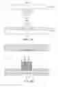
FIGS. 1A through 1I are schematic cross-sectional views illustrating the process of manufacturing a substrate for flip chip, according to an exemplary embodiment of the present invention.
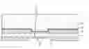
As shown in FIG. 1A, at least one conductive pad 2 is formed on a prepared base substrate 1. Here, the conductive pad 2 may be formed by using a photolithography process. The base substrate 1 may utilize a semiconductor substrate or a package substrate.
A photosensitive resin layer (not shown) is applied on the base substrate 1 including a conductive pad material (not shown) applied thereon. Subsequently, the conductive pad 2 may be formed by using the photolithography process for exposing and developing the applied photosensitive resin layer using a mask (not shown) having a predetermined pattern.
Thereafter, a solder resist layer 3, having a first opening V1 (not shown) exposing the conductive pad 2, is formed on the base substrate 1 including the conductive pad 2.
Here, the first opening V1 may be formed by exposing and developing a solder resist layer 3, applied on the base substrate 1, by using a predetermined mask pattern (not shown).
Also, an opening “O”, corresponding to a solder pad connected to a mother board or the like, may be then formed.
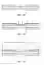
Subsequently, as shown in FIG. 1B, a seed layer 4 for plating may be formed on the solder resist layer 3. The seed layer 4 for plating may be formed in the case that a metal post 6, depicted in FIG. 1E, is formed using an electro-plating method. The formation method for the metal post 6 is not limited thereto, and an electroless plating method may be used to form the metal post 6. As described above, if the metal post 6 is formed using the electroless plating method, the seed layer 4 for plating may not be formed.
Thereafter, as shown in FIG. 1C, a dry film 5′ is applied to the seed layer 4 for plating.
Here, the dry film 5′ utilizes a high heat resistant film in order to endure a reflow process performed at a high temperature of 260° C. or higher. In addition, the dry film 5′ may have a thickness of 60 μm or greater for the purpose of forming a post bump with an appropriate height.
Thereafter, as shown in FIG. 1D, the dry film 5′, depicted in FIG. 1C, is subjected to exposing and developing processes, thereby forming a dry film 5 having a second opening V2 communicating (i.e., connected) with the first opening V1.
The second opening V2 may be formed by exposing and developing the photosensitive dry film 5′, applied on the seed layer 4 for plating, by using a predetermined mask pattern (not shown), in the same manner as the first opening V1 is formed.
Thereafter, as shown in FIG. 1E, the metal post 6 is formed in the first opening V1 and at least a part of the second opening V2.
At this time, the metal post 6 may be formed by using an electro-plating method or an electroless plating method.
The metal post 6 fills the first opening V1 and a part of the second opening V2 in order to cause wiring patterns to have fine pitches, enable high-speed signal transmissions between a substrate and a semiconductor chip, ensure a sufficient interval between chips, and perform a heat dissipation function. In this case, the metal post 6 may have a cylindrical structure. Also, the metal post 6 may be formed of a conductive material such as copper (Cu). However, the material of the metal post 6 is not limited to the material described, and may utilize nickel (Ni), tin (Sn), gold (Au) or the like.
Here, the metal post 6, when formed of copper, can lower the overall electrical resistance of the substrate 1 for flip chip due to the low resistance of copper, and can also enhance heat dissipation characteristics. Furthermore, the flexural deformation of the substrate 10 for flip chip can be prevented since copper is a metal with a relatively high level of rigidity and thus can retain its rigidity even after undergoing a plurality of high-temperature processes for forming the substrate 10 for flip chip.
In this case, the height of the metal post 6 is not limited specifically, but may satisfy the condition of H/D>1 where H denotes the height of the metal post and D denotes the diameter of the metal post. The metal post 6 may be formed to have a height of 50 μm or greater. Also, the metal post 6 may be formed to have a diameter of 30 μm or greater.
Thereafter, as shown in FIG. 1F, the second opening V2 above the metal post 6 is filled with solder paste. The solder paste is then subject to a reflow processes, thereby forming a solder cap 7a.
In this case, the solder paste may be filled up to a level higher than the second opening V2.
Subsequently, as shown in FIG. 1G, the surface of the solder cap 7a is mechanically or chemically polished to thereby form a planarized solder cap 7b.
Accordingly, the overall height of the metal post 6 and the solder cap 7b can attain uniformity even if the metal post 6 itself has a non-uniform height due to a variation in plating thickness occurring in the previous process of forming the metal post 6.
Namely, the solder cap 7b serves to ensure uniformity in height, as well as to perform a buffering function during a packaging process for the substrate 10 for flip chip.
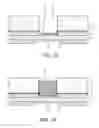
Thereafter, a typical deflux process is carried out to remove flux remaining on the planarized solder cap 7b.
Thereafter, as shown in FIG. 1H, the dry film 5 is stripped off.
Here, the dry film 5 may be removed by causing the dry film 5 on the surface of the base substrate 1 to contact a solvent. As for this contact method, the base substrate 1 may be immersed in a solvent, or a solvent may be sprayed onto the base substrate 1. In addition, the dry film 5 may be removed by controlling the temperature and contact duration with a solvent. Alternatively, the base substrate 1 may be cleaned using ultrasonic waves while being immersed in a solvent. In this case, the time it takes to remove the dry film 5 can be shortened as compared to when the dry film 5 on the surface of the base substrate 1 simply comes in contact with a solvent.
Thereafter, as shown in FIG. 1I, the seed layer 4 for plating is removed to thereby manufacture a substrate 10 for flip chip.
The substrate 10 for flip chip, manufactured according to the process of manufacturing the substrate 10 for flip chip according to an exemplary embodiment of the present invention, includes a base substrate 1 including at least one conductive pad 2, a solder resist layer 3 formed on the base substrate 1 and having a first opening V1 exposing the conductive pad 1, a metal post 6 filling at least a part of the first opening V1, and a solder cap 7b formed on the metal post and having a planarized surface.
Here, the metal post 6 may be formed by an electro-plating method or an electroless plating method.
The metal post 6 serves to enable wiring patterns to have fine pitches, allow for high-speed signal transmission between a substrate and a semiconductor chip, ensure distances between chips, and perform a heat dissipation function. The metal post 6 fills at least a part of the first opening V1. In this case, the metal post 6 may have a cylindrical structure. The metal post 6 may be formed of a conductive material such as copper (Cu), but is not limited thereto. The metal post 6 may be formed of a material such as nickel (Ni), tin (Sn), gold (Au) or the like.
Here, the metal post 6, when formed of copper, may lower the overall electric resistance of the substrate 10 for flip chip due to the low resistance characteristic of copper, and may also improve its heat dissipation characteristic. Since copper is a metal with a high level of rigidity, it can retain its rigidity even after a plurality of high-temperature processes for forming the substrate 10 for flip chip, thereby preventing the flexural deformation of the substrate 10 for flip chip.
The height of the metal post 6 is not limited specifically. However, the metal post 6 may be formed to satisfy the condition of H/D>1 where H denotes the height of the metal post 6, and D denotes the diameter of the metal post 6. Furthermore, the metal post 6 may have a height of 50 μm or greater. Also, the metal post 6 may have a diameter of 30 μm or greater.
The solder cap 7b is a planarized version of the solder cap 7a, which results from the mechanical or chemical polishing of the surface of the solder cap 7a.
Accordingly, even if the height of the metal post 6 is non-uniform due to a variation in plating thickness caused during the previous process of forming the metal post 6, the planarized solder cap 7b may supplement this non-uniformity, and thus allows for the uniformity of the overall height of the metal post 6 and the solder cap 7b.
That is, the solder cap 7b serves to ensure height uniformity, as well as to perform a buffering function during the packaging process of the substrate 10 for flip chip.
According to the present invention, there are provided a substrate for flip chip, enabling the formation of fine pitches and having improved reliability, and a method of manufacturing the same.
Furthermore, the use of the metal post and the solder cap solves the non-uniformity in height and location. Thus, the metal post, capable of providing improved height uniformity and mounting reliability, may be applied not only to a semiconductor substrate but also to a package substrate.
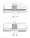
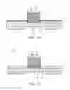
FIGS. 2A and 2B are schematic cross-sectional views for comparing a bonding part between a substrate for flip chip, formed according to an exemplary embodiment of the present invention, and another substrate with a bonding part between a related art substrate for flip chip and another substrate.
Referring to FIG. 2A, a related art substrate 100a, including a solder bump 60a connected with a solder pad 20a in a solder resist layer 300 including an opening, is soldered on a chip substrate 100b. In this case, typically, the chip substrate 100b includes, for the enhancement of assemblage, a metal pad 20b and a solder bump 60a formed on the metal pad 20b, and the chip substrate 100b is then soldered with the substrate 100a.
However, as shown in FIG. 2B, the substrate 10 for flip chip, according to this exemplary embodiment, includes the metal post 6 and the solder cap 7b formed on the metal post 6. Accordingly, when the substrate 10 for flip chip, having the vertically elongated metal post 6 as compared to the related art, is soldered on the metal pad 2′ formed on the chip substrate 1′, assembly defects can be reduced even without a solder bump formed on the chip substrate 1′.
Accordingly, a defect ratio, involving failed soldering, can be reduced even when solder bumps are not formed on both the substrate 10 for flip chip and another component or a chip substrate. This is contributive to reducing manufacturing costs.
As set forth above, according to exemplary embodiments of the invention, there can be provided the method of manufacturing a substrate for flip chip, capable of achieving fine pitches and improved reliability, and the substrate for flip chip manufactured using the same.
Furthermore, the metal post and the solder cap are used to reduce non-uniformity in height and location. Thus, a package substrate, as well as a semiconductor substrate, can be provided with a metal post allowing for the enhancement of high uniformity and mounting reliability.
Also, defect generation, involving failed soldering, can be reduced even when solder bumps are not formed on both the substrate for flip chip and another component or a chip substrate. This is contributive to reducing manufacturing costs.
While the present invention has been shown and described in connection with the exemplary embodiments, it will be apparent to those skilled in the art that modifications and variations can be made without departing from the spirit and scope of the invention as defined by the appended claims.
Claims
What is claimed is:1. A method of manufacturing a substrate for flip chip, the method comprising:
providing a base substrate including at least one conductive pad;
forming a solder resist layer on the base substrate, the solder resist layer including a first opening exposing the conductive pad;
forming a dry film on the solder resist layer, the dry film including a second opening connected with the first opening;
forming a metal post in the first opening and a part of the second opening;
filling the second opening above the metal post with solder paste;
forming a solder cap by performing a reflow process on the filled solder paste;
planarizing a surface of the solder cap; and
removing the dry film.
2. The method of claim 1, wherein the metal post is formed to satisfy a condition of H/D>1 where H denotes a height of the metal post and D denotes a diameter of the metal post.
3. The method of claim 1, wherein the metal post is formed to have a height of 50 μm or greater.
4. The method of claim 1, wherein the metal post is formed by using an electroless plating method.
5. The method of claim 1, further comprising forming a seed layer for plating on the solder resist layer after the forming of the solder resist layer.
6. The method of claim 5, wherein the metal post is formed by using an electro-plating method.
7. The method of claim 1, further comprising removing the seed layer for plating after the removing of the dry film.
8. The method of claim 1, further comprising performing a deflux process on the solder cap after the forming of the solder cap.
9. A substrate for flip chip, the substrate comprising:
a base substrate including at least one conductive pad;
a solder resist layer formed on the base substrate and having an opening exposing the conductive pad;
a metal post filling at least a part of the opening; and
a solder cap formed on the metal post and having a planarized surface.
10. The substrate of claim 9, wherein the metal post satisfies a condition of H/D>1 where H denotes a height of the metal post and D denotes a diameter of the metal post.
11. The substrate of claim 9, wherein the metal post has a height of 50 μm or greater.
12. The substrate of claim 9, wherein the metal post is formed by an electroless plating method.
13. The substrate of claim 9, further comprising a seed layer for plating on an interface between the opening and the metal post within the opening.
14. The substrate of claim 13, wherein the metal post is formed by using an electro-plating method.
15. A method of manufacturing a package substrate, the method comprising:
providing a base substrate including at least one conductive pad;
forming a solder resist layer on the base substrate, the solder resist layer including a first opening exposing the conductive pad;
forming a dry film on the solder resist layer, the dry film including a second opening connected with the first opening;
forming a metal post in the first opening and a part of the second opening;
filling the second opening above the metal post with solder paste;
forming a solder cap by performing a reflow process on the filled solder paste;
planarizing a surface of the solder cap;
removing the dry film;
providing a chip substrate including at least one metal pad; and
bonding the base substrate with the chip substrate such that the solder cap having the planarized surface corresponds to the metal pad.
16. The method of claim 15, wherein the metal post is formed to satisfy a condition H/D>1 where H denotes a height of the metal post and D denotes a diameter of the metal post.
17. The method of claim 15, wherein the metal post is formed to have a height of 50 μm or greater.
18. A package substrate comprising:
a base substrate including at least one conductive pad;
a solder resist layer formed on the base substrate and having an opening exposing the conductive pad;
a metal post filling at least a part of the opening;
a solder cap formed on the metal post and having a planarized surface; and
a chip substrate including at least one metal pad and bonded with the base substrate such that the metal pad corresponds to the solder cap having the planarized surface.
19. The package substrate of claim 18, wherein the metal post satisfies a condition of H/D>1 where H denotes a height of the metal post and D denotes a diameter of the metal post.
20. The package substrate of claim 18, wherein the metal post has a height of 50 μm or greater.
Images & Drawings included:
Sources:
- United States Patent and Trademark Office - verify current appl. status at the USPTO↗
Similar patent applications:
Recent applications in this class:
- » 20250185180 2025-06-05
PRINTED CIRCUIT BOARD AND MANUFACTURING METHOD THEREOF - » 20250126722 2025-04-17
CIRCUIT COMPENSATION METHOD APPLIED TO PATTERN DISPLACEMENT AND CIRCUIT STRUCTURE - » 20250107008 2025-03-27
PRINTED CIRCUIT BOARD - » 20250098076 2025-03-20
BOARD AND ELECTRONIC DEVICE - » 20240188224 2024-06-06
Electrical devices with electrodes on softening polymers and methods of manufacturing thereof - » 20240164026 2024-05-16
PRINTED CIRCUIT BOARD - » 20240107683 2024-03-28
WIRING CIRCUIT BOARD - » 20230180396 2023-06-08
Electrical devices with electrodes on softening polymers and methods of manufacturing thereof - » 20230007787 2023-01-05
Flux dotting tool - » 20220377910 2022-11-24
PREPARATION METHOD FOR CONNECTOR ELECTRONIC DEVICE CONNECTOR AND APPLICATION THEREOF
Recent applications for this Assignee:
- » 20170293104 2017-10-12
Lens module - » 20160242284 2016-08-18
PRINTED CIRCUIT BOARD HAVING METAL BUMPS - » 20160148750 2016-05-26
COIL COMPONENT - » 20160126745 2016-05-05
Non-contact type power transmitting apparatus, non-contact type power receiving apparatus, and non-contact type power transceiving apparatus - » 20160088201 2016-03-24
CAMERA MODULE - » 20160037624 2016-02-04
FLEXIBLE PRINTED CIRCUIT BOARD AND MANUFACTURING METHOD THEREOF - » 20150373842 2015-12-24
SUBSTRATE STRIP, SUBSTRATE PANEL, AND MANUFACTURING METHOD OF SUBSTRATE STRIP - » 20150364992 2015-12-17
Charge pump system and charge pump protection circuit - » 20150364585 2015-12-17
POWER SEMICONDUCTOR DEVICE - » 20150355777 2015-12-10
Integration circuit, touch interaction sensing apparatus, and touchscreen apparatus