Chip package and method for forming the same
US20110227210A1
2011-09-22
13/049,528
2011-03-16
✅ Patent granted
US 8,530,985 B2
2013-09-10
-
-
Nitin Parekh
Birch, Stewart, Kolasch & Birch, LLP
2031-09-29
Abstract:
An embodiment of the invention provides a chip package, which includes: a substrate having an upper surface and a lower surface; a passivation layer located overlying the upper surface of the substrate; a plurality of conducting pad structures disposed overlying the upper surface of the substrate, wherein at least portions of upper surfaces of the conducting pad structures are exposed; a plurality of openings extending from the upper surface towards the lower surface of the substrate; and a plurality of movable bulks located between the openings and connected with the substrate, respectively, wherein each of the movable bulks is electrically connected to one of the conducting pad structures.
Applicant:
Interested in similar patents?
Get notified when new applications in this technology area are published.
Classification:
H01L29/84 IPC
Semiconductor devices adapted for rectifying, amplifying, oscillating or switching, or capacitors or resistors with at least one potential-jump barrier or surface barrier, e.g. PN junction depletion layer or carrier concentration layer; Details of semiconductor bodies or of electrodes thereof; Multistep manufacturing processes therefor; Types of semiconductor device ; Multistep manufacturing processes therefor controllable by variation of applied mechanical force, e.g. of pressure
H01L2224/48 » CPC further
Indexing scheme for arrangements for connecting or disconnecting semiconductor or solid-state bodies and methods related thereto as covered by; Means for bonding being attached to, or being formed on, the surface to be connected, e.g. chip-to-package, die-attach, "first-level" interconnects; Manufacturing methods related thereto; Wire connectors; Manufacturing methods related thereto; Structure, shape, material or disposition of the wire connectors after the connecting process of an individual wire connector
H01L2924/12041 » CPC further
Indexing scheme for arrangements or methods for connecting or disconnecting semiconductor or solid-state bodies as covered by; Details of semiconductor or other solid state devices to be connected; Device type; Passive devices, e.g. 2 terminal devices; Optical Diode LED
H01L2924/1461 » CPC further
Indexing scheme for arrangements or methods for connecting or disconnecting semiconductor or solid-state bodies as covered by; Details of semiconductor or other solid state devices to be connected; Mixed devices MEMS
H01L2924/15788 » CPC further
Indexing scheme for arrangements or methods for connecting or disconnecting semiconductor or solid-state bodies as covered by; Details of package parts other than the semiconductor or other solid state devices to be connected; Die mounting substrate; Material with a principal constituent of the material being a non metallic, non metalloid inorganic material Glasses, e.g. amorphous oxides, nitrides or fluorides
H01L2224/45099 » CPC further
Indexing scheme for arrangements for connecting or disconnecting semiconductor or solid-state bodies and methods related thereto as covered by; Means for bonding being attached to, or being formed on, the surface to be connected, e.g. chip-to-package, die-attach, "first-level" interconnects; Manufacturing methods related thereto; Wire connectors; Manufacturing methods related thereto; Structure, shape, material or disposition of the wire connectors prior to the connecting process of an individual wire connector; Core members of the connector Material
H01L2924/00014 » CPC further
Indexing scheme for arrangements or methods for connecting or disconnecting semiconductor or solid-state bodies as covered by; Technical content checked by a classifier the subject-matter covered by the group, the symbol of which is combined with the symbol of this group, being disclosed without further technical details
H01L2924/14 » CPC further
Indexing scheme for arrangements or methods for connecting or disconnecting semiconductor or solid-state bodies as covered by; Details of semiconductor or other solid state devices to be connected; Device type Integrated circuits
H01L2924/00 » CPC further
Indexing scheme for arrangements or methods for connecting or disconnecting semiconductor or solid-state bodies as covered by
H01L23/49 IPC
Details of semiconductor or other solid state devices; Arrangements for conducting electric current to or from the solid state body in operation, e.g. leads, terminal arrangements ; Selection of materials therefor consisting of soldered constructions wire-like arrangements or pins or rods
H01L21/78 IPC
Processes or apparatus adapted for the manufacture or treatment of semiconductor or solid state devices or of parts thereof; Manufacture or treatment of devices consisting of a plurality of solid state components formed in or on a common substrate or of parts thereof; Manufacture of integrated circuit devices or of parts thereof; Manufacture or treatment of devices consisting of a plurality of solid state components or integrated circuits formed in, or on, a common substrate with subsequent division of the substrate into plural individual devices
H01L24/85 » CPC main
Arrangements for connecting or disconnecting semiconductor or solid-state bodies; Methods or apparatus related thereto; Methods for connecting semiconductor or other solid state bodies using means for bonding being attached to, or being formed on, the surface to be connected using a wire connector
B81B7/007 » CPC further
Microstructural systems; Auxiliary parts of microstructural devices or systems; Packages or encapsulation Interconnections between the MEMS and external electrical signals
B81C2203/0118 » CPC further
Forming microstructural systems; Packaging MEMS Bonding a wafer on the substrate, i.e. where the cap consists of another wafer
H01L24/45 » CPC further
Arrangements for connecting or disconnecting semiconductor or solid-state bodies; Methods or apparatus related thereto; Means for bonding being attached to, or being formed on, the surface to be connected, e.g. chip-to-package, die-attach, "first-level" interconnects; Manufacturing methods related thereto; Wire connectors; Manufacturing methods related thereto; Structure, shape, material or disposition of the wire connectors prior to the connecting process of an individual wire connector
H01L2224/85 » CPC further
Indexing scheme for arrangements for connecting or disconnecting semiconductor or solid-state bodies and methods related thereto as covered by; Methods for connecting semiconductor or other solid state bodies using means for bonding being attached to, or being formed on, the surface to be connected using a wire connector
H01L23/48 IPC
Details of semiconductor or other solid state devices Arrangements for conducting electric current to or from the solid state body in operation, e.g. leads, terminal arrangements ; Selection of materials therefor
Description
CROSS REFERENCE
This application claims the benefit of U.S. Provisional Application No. 61/315,220, filed on Mar. 18, 2010, the entirety of which is incorporated by reference herein.
BACKGROUND OF THE INVENTION
1. Field of the Invention
The present invention relates to a chip package, and in particular relates to a MEMS chip package.
2. Description of the Related Art
With the advancements in technology, the packaging process of chips has become more complex and now require heavy and complicated patterning processes, including an etching process. In addition, formed chip packages often need to be integrated with another electronic device for different applications.
Thus, it is desired to have a more simple chip packaging process, wherein not only are devices (such as conducting pads) protected from damage, but also the integration between the chip package and other electronic devices are simplified.
BRIEF SUMMARY OF THE INVENTION
An embodiment of the invention provides a chip package, which includes: a substrate having an upper surface and a lower surface; a passivation layer located overlying the upper surface of the substrate; a plurality of conducting pad structures disposed overlying the upper surface of the substrate, wherein at least portions of upper surfaces of the conducting pad structures are exposed; a plurality of openings extending from the upper surface towards the lower surface of the substrate; and a plurality of movable bulks located between the openings and connected with the substrate, respectively, wherein each of the movable bulks is electrically connected to one of the conducting pad structures.
An embodiment of the invention provides a method for forming a chip package, which includes: providing a substrate having at least a device region and a pad region, wherein a plurality of conducting pad structures are disposed overlying the pad region of the substrate, a passivation layer and an etch stop layer are sequentially disposed overlying an upper surface of the substrate, and the passivation layer and the etch stop layer have a plurality of openings on the device region, wherein the openings expose the upper surface of the substrate; using the etch stop layer as a mask to remove a portion of the substrate to form a plurality of openings and a plurality of movable bulks between the openings, wherein the openings extend from the upper surface towards a lower surface of the substrate, the movable bulks connect with the substrate, and each of the movable bulks is electrically connected to one of the conducting pad structures; and removing the etch stop layer.
A detailed description is given in the following embodiments with reference to the accompanying drawings.
BRIEF DESCRIPTION OF THE DRAWINGS
The present invention can be more fully understood by reading the subsequent detailed description and examples with references made to the accompanying drawings, wherein:
FIGS. 1A-1F are cross-sectional views showing the steps of forming a chip package according to an embodiment of the present invention; and
FIG. 2 is a top view partially showing a chip package according to an embodiment of the present invention.
DETAILED DESCRIPTION OF THE INVENTION
The following description is of the best-contemplated mode of carrying out the invention. This description is made for the purpose of illustrating the general principles of the invention and should not be taken in a limiting sense. The scope of the invention is best determined by reference to the appended claims.
It is understood, that the following disclosure provides many different embodiments, or examples, for implementing different features of the invention. Specific examples of components and arrangements are described below to simplify the present disclosure. These are, of course, merely examples and are not intended to be limiting. In addition, the present disclosure may repeat reference numbers and/or letters in the various examples. This repetition is for the purpose of simplicity and clarity and does not in itself dictate a relationship between the various embodiments and/or configurations discussed. Furthermore, descriptions of a first layer “on,” “overlying,” (and like descriptions) a second layer include embodiments where the first and second layers are in direct contact and those where one or more layers are interposing the first and second layers.
A chip package according to an embodiment of the present invention may be used to package a micro electro mechanical system chip. However, embodiments of the invention are not limited thereto. For example, the chip package of the embodiments of the invention may be applied to active or passive devices, or electronic components with digital or analog circuits, such as opto electronic devices, micro electro mechanical systems (MEMS), micro fluidic systems, and physical sensors for detecting heat, light, or pressure. Particularly, a wafer scale package (WSP) process may be applied to package semiconductor chips, such as image sensor devices, light-emitting diodes (LEDs), solar cells, RF circuits, accelerators, gyroscopes, micro actuators, surface acoustic wave devices, pressure sensors, or ink printer heads.
The wafer scale package process mentioned above mainly means that after the package process is accomplished during the wafer stage, the wafer with chips is cut to obtain separate independent packages. However, in a specific embodiment, separate independent chips may be redistributed overlying a supporting wafer and then be packaged, which may also be referred to as a wafer scale package process. In addition, the above mentioned wafer scale package process may also be adapted to form chip packages of multi-layer integrated circuit devices by stacking a plurality of wafers having integrated circuits.
In the following description, a MEMS chip package is taken as an example with references made to the accompanying drawings to illustrate a chip package according to an embodiment of the invention. For example, in one embodiment, the packaged MEMS chip may include an accelerator.
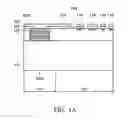
FIGS. 1A-1F are cross-sectional views showing the steps of forming a chip package according to an embodiment of the present invention. As shown in FIG. 1A, a substrate 100 is provided, which has at least a device region 101 and at least a pad region 103. The substrate 100 includes, for example, a semiconductor material or a ceramic material. In one embodiment, the substrate 100 is a semiconductor wafer such as a silicon wafer, and thus a wafer-level package process may be performed. Fabrication cost and fabrication time may be reduced if a chip package is formed by a wafer-level package process.
As shown in FIG. 1A, in one embodiment, the pad region 103 of the substrate 100 has a plurality of conducting pad structures 102 which are disposed overlying the upper surface 100a of the substrate 100. Although only a conducting pad is shown in FIG. 1A, one skilled in the art should understand that a plurality of pads may be stacked and/or arranged on the substrate 100. For example, in one embodiment, the pad region 103 surrounds the device region 101. The pad region 103 has a plurality of conducting pad structures 102 which also surround the device region 101. In addition, in one embodiment, the conducting pad structure 102 is a plurality of conducting pads which are stacked with each other, at least a conducting pad, or a conducting pad structure constructed of at least a conducting pad and at least an interconnection structure. The conducting pads may be formed in, for example, a dielectric layer 105 in the substrate 100 and electrically connected to each other through interconnections formed in the dielectric layer 105.
As shown in FIG. 1A, in one embodiment, a passivation layer 104 and an etch stop layer 106 are subsequently disposed overlying the upper surface 100a of the substrate 100. Typically, a semiconductor wafer fabricated by a wafer fabrication facility is covered by a chip passivation layer such as the passivation layer 104. Meanwhile, in order to form electrical connections between the devices inside the chip and the external circuits, the passivation layer is typically defined to form a plurality of openings exposing the conducting pad structure 102.
As shown in FIG. 1A, the passivation layer 104 and the etch stop layer 106 arc patterned to have a plurality of openings 108 exposing the substrate 100 thereunder. In addition, in one embodiment, a plurality of conducting wires 110 may be on the substrate 100 between the openings 108. These conducting wires 110 are electrically connected to the corresponding conducting pad structures 102, respectively. The conducting wire 110 may be formed overlying, for example, the upper surface 100a of the substrate 100 and be covered by the passivation layer 104. Alternatively, the conducting wire 110 may also be formed in the dielectric layer 105 of the substrate 100. In this case, the dielectric layer 105 is regarded as a portion of the substrate 100, and the upper surface of the dielectric layer 105 is regarded as the upper surface 100a of the substrate 100. The conducting wire 110 may be, for example, a conducting wire formed of a metal material. Alternatively, in one embodiment, the conducting wire 110 includes an elastic conducting structure formed of a semiconductor material. For example, a portion of the semiconductor substrate may be patterned to be a structure similar to a spring by a patterning process. In one embodiment, the conducting wire 110 is electrically connected to the substrate 100.
Then, referring to FIG. 1B, note that the dielectric layer 105 and the plurality of conducting pad are not shown in the drawing for the purpose of convenience, and a single-layer conducting pad structure 102 is shown in the drawing for simplicity. As shown in FIG. 1B, the etch stop layer 106 is used as a mask and a portion of the substrate 100 is removed from the upper surface 100a of the substrate 100 exposed by the openings 108 to form a plurality of openings 112 by, for example, an etching process, and a plurality of movable bulks 114 are formed between the openings 112. That is, the remaining substrate between the openings 112 has reduced constraint and thus become the movable bulks 114 which can move, bend, or vibrate if an external force is applied.
As shown in FIG. 1B, in one embodiment, the etch stop layer 106 may be removed after the openings 112 are formed. In another embodiment, when the substrate 100 is partially removed to form the openings 112, simultaneously, the etch stop layer 106 is etched. That is, in the etching process, the etchant which is used has a higher etchant rate for the substrate 100 than that for the etch stop layer 106. In one embodiment, a material of the etch stop layer 106 may be, for example, an oxide. In one embodiment, by tuning the material, thickness, and/or etching conditions of the etching stop layer 106, the etch stop layer 106 may be substantially and completely removed from the substrate 100 after the openings 112 have been formed. In this case, the upper surfaces of the conducting pad structures 102 are at least partially exposed.
As shown in FIG. 1B, in one embodiment, the opening 112 extends from the upper surface 100a towards the lower surface 100b of the substrate 100. In addition, each of the movable bulks 114 is electrically connected to one of the conducting pad structures 102 correspondingly. For example, the movable bulk 114 may be electrically connected to the conducting pad structure 102 through the conducting wire 110 thereon. In one embodiment, the movable bulk 114 connects with the substrate 100, and the materials of the movable bulk 114 and the substrate 100 are the same, as shown in FIG. 1B. For example, both the materials of the substrate 100 and the movable bulk 114 may include a semiconductor material.
FIG. 2 is a top view partially showing a chip package according to an embodiment of the present invention. When the chip package is applied by an external force and moves acceleratedly, the movable bulks 114 will bend due to the external force such that relative distances between the movable bulks 114 are changed. The changes of the relative distances cause changes in capacitance values. Thus, signals of the changes in capacitance values may be transmitted out through the conducting pad structures 102 electrically connected to the movable bulks 114.
In one embodiment, in order to increase the displacement of the movable bulks 114 to improve the sensitivity when an external force is applied thereto, an effort may be made to connect the openings 112. That is, percentage of the connection portions between the movable bulks 114 and the substrate 100 is reduced such that the freedom of vibration or movement of the movable bulks 114 is increased. For example, a trench may be formed from the lower surface 100b of the substrate 100 to expose the openings 112.
In one embodiment, before the trench connecting the openings 112 is formed, a package layer may be optionally disposed overlying the upper surface 100a of the substrate 100. For example, referring to FIG. 1C, a package layer 116 is provided and disposed overlying the upper surface 100a of the substrate 100. The package layer 116 may be, for example, a transparent substrate or a semiconductor substrate. In one embodiment, the package layer 116 may be a glass substrate or a silicon wafer. The package layer 116 may be used to protect the chip thereunder.
As shown in FIG. 1C, in one embodiment, a spacer layer 118 may be optionally disposed between the package layer 116 and the substrate 100. The spacer layer 118 may be an insulating material, for example. In one embodiment, the spacer layer 118, the substrate 100, and the package layer 116 together form a cavity 120. The opening 112 and the movable bulks 114 are located underlying the cavity 120. In one embodiment, the spacer layer 118 is disposed to surround the device region 101. Thus, the formed cavity is a substantially airtight cavity. Next, as shown in FIG. 1C, the substrate 100 may be optionally thinned from the lower surface 100b of the substrate 100 by, for example, mechanical grinding or chemical mechanical polishing.
Next, as shown in FIG. 1D, a trench 122 is formed from the lower surface 100b of the substrate 100. The bottom portion of the trench 122 exposes the openings 112 such that the openings 112 connect with each other. After the trench 122 is formed, the movable bulks 114 connect with the substrate 100 only through the periphery portions (not shown). Thus, when the chip package is applied by an external force and moves acceleratedly, the movable bulks 114 will bend or move in response to the external force more easily such that the sensing sensitivity is increased.
Next, as shown in FIG. 1E, a portion of the package layer 116 may be optionally removed such that the conducting pad structure 102 is not completely covered by the package layer 116. After the conducting pad structure 102 is at least partially exposed, it is easier for the conducting pad structure 102 to connect with another conducting structure.
For example, as shown in FIG. 1F, in one embodiment, a conducting structure 124 may be formed overlying the conducting pad structure 102. The conducting structure 124 may be used to provide electrical connections between the chip package and another electronic device. The conducting structure 124 may be, for example, a bonding wire. Alternatively, in another embodiment, a through-substrate via may be formed under the bottom portion of the conducting pad structure 102 to serve as the conducting structure 124.
In one embodiment, the substrate 100 is a semiconductor wafer such as a silicon wafer. A plurality of structures similar to the structure shown in FIG. 1F are formed on the semiconductor wafer. In this case, the substrate 100 may be diced along predetermined scribe lines (not shown) on the substrate 100 to form a plurality of separate chip packages.
Embodiments of the invention have many variations. For example, in one embodiment, the passivation layer is not like the structure shown in FIG. 1A to cover a portion of the conducting pad structure 102. In this case, the upper surface of the conducting pad of the formed chip package substantially does not directly contact with any insulating material.
In embodiments of the invention, the etch stop layer is formed overlying the substrate such that the conducting pad structure is protected during the forming of the movable bulks, which prevents the conducting pad from being damaged due to the etching process. In addition, the etch stop layer may also be used as an etch mask for defining the openings surrounding the movable bulks. Further, the conducting pad structure of the chip package according to an embodiment of the invention is at least partially exposed such that the chip package may be connected with another conducting wire which facilitates integration with other electronic devices.
While the invention has been described by way of example and in terms of the preferred embodiments, it is to be understood that the invention is not limited to the disclosed embodiments. To the contrary, it is intended to cover various modifications and similar arrangements (as would be apparent to those skilled in the art). Therefore, the scope of the appended claims should be accorded the broadest interpretation so as to encompass all such modifications and similar arrangements.
Claims
What is claimed is:1. A chip package, comprising:
a substrate having an upper surface and a lower surface;
a passivation layer located overlying the upper surface of the substrate;
a plurality of conducting pad structures disposed overlying the upper surface of the substrate, wherein at least portions of upper surfaces of the conducting pad structures are exposed;
a plurality of openings extending from the upper surface towards the lower surface of the substrate; and
a plurality of movable bulks located between the openings and connected with the substrate, respectively, wherein each of the movable bulks is electrically connected to one of the conducting pad structures.
2. The chip package as claimed in claim 1, wherein the openings connect with each other.
3. The chip package as claimed in claim 1, further comprising a trench extending from the lower surface towards the upper surface of the substrate, wherein a bottom portion of the trench exposes the openings.
4. The chip package as claimed in claim 1, further comprising a package layer disposed overlying the upper surface of the substrate.
5. The chip package as claimed in claim 4, wherein the package layer does not completely cover the conducting pad structures.
6. The chip package as claimed in claim 4, wherein the package layer does not cover the conducting pad structures.
7. The chip package as claimed in claim 4, further comprising a spacer layer disposed between the upper surface of the substrate and the package layer.
8. The chip package as claimed in claim 7, wherein the substrate, the spacer layer, and the passivation layer together form a cavity, and the openings and the movable bulks are located underlying the cavity.
9. The chip package as claimed in claim 1, further comprising a conducting structure electrically connected to the conducting pad structures.
10. The chip package as claimed in claim 9, wherein the conducting structure comprises a bonding wire.
11. The chip package as claimed in claim 1, further comprising a plurality of conducting wires respectively and correspondingly located on the movable bulks, wherein the conducting wires electrically connect the movable bulks and the conducting pad structures, respectively and correspondingly.
12. A method for forming a chip package, comprising:
providing a substrate having at least a device region and a pad region, wherein a plurality of conducting pad structures are disposed overlying the pad region of the substrate, a passivation layer and an etch stop layer are sequentially disposed overlying an upper surface of the substrate, and the passivation layer and the etch stop layer have a plurality of openings on the device region, wherein the openings expose the upper surface of the substrate;
using the etch stop layer as a mask to remove a portion of the substrate to form a plurality of openings and a plurality of movable bulks between the openings, wherein the openings extend from the upper surface towards a lower surface of the substrate, the movable bulks connect with the substrate, and each of the movable bulks is electrically connected to one of the conducting pad structures; and
removing the etch stop layer.
13. The method for forming a chip package as claimed in claim 12, wherein during the step of removing the portion of the substrate to form the openings, the etch stop layer is removed simultaneously and gradually.
14. The method for forming a chip package as claimed in claim 13, wherein after the openings are formed, the etch stop layer are substantially and completely removed from the substrate.
15. The method for forming a chip package as claimed in claim 12, further comprising forming a trench from the lower surface of the substrate, wherein a bottom portion of the trench exposes the openings.
16. The method for forming a chip package as claimed in claim 12, further comprising disposing a package layer overlying the upper surface of the substrate.
17. The method for forming a chip package as claimed in claim 16, further comprising disposing a spacer layer between the package layer and the substrate.
18. The method for forming a chip package as claimed in claim 16, further comprising removing a portion of the package layer to expose the conducting pad structures.
19. The method for forming a chip package as claimed in claim 12, wherein the substrate comprises a semiconductor wafer.
20. The method for forming a chip package as claimed in claim 12, further comprising dicing the substrate along at least a predetermined scribe line of the substrate.
Images & Drawings included:


Sources:
- United States Patent and Trademark Office - verify current appl. status at the USPTO↗
Similar patent applications:
- » 20210082861
Chip package, method of forming a chip package and method of forming an electrical contact - » 20220139798
Method of forming a chip package, method of forming a semiconductor arrangement, chip package, and semiconductor arrangement - » 20250079330
EMBEDDED CHIP-PACKAGE, SEMICONDUCTOR PACKAGE, METHOD OF FORMING AN EMBEDDED CHIP-PACKAGE, METHOD OF FORMING A SEMICONDUCTOR PACKAGE, AND METHOD OF ANALYZING AN EMBEDDED CHIP-PACKAGE OR A SEMICONDUCTOR PACKAGE - » 20240087992
CHIP PACKAGE, CHIP SYSTEM, METHOD OF FORMING A CHIP PACKAGE, AND METHOD OF FORMING A CHIP SYSTEM - » 20130256855
Chip arrangement, a method for forming a chip arrangement, a chip package, a method for forming a chip package - » 20230274996
CHIP ARRANGEMENT, CHIP PACKAGE, METHOD OF FORMING A CHIP ARRANGEMENT, AND METHOD OF FORMING A CHIP PACKAGE - » 20220173074
Chip Package and Method of Forming Chip Packages - » 20220208733
Chip Package and Method of Forming Chip Packages - » 20240105678
CHIP PACKAGE, METHOD OF FORMING A CHIP PACKAGE, AND CHIP SYSTEM - » 20170338169
Chip package and method of forming a chip package with a metal contact structure and protective layer, and method of forming an electrical contact
Recent applications in this class:
- » 20250266392 2025-08-21
Semiconductor packaging method and semiconductor packaging structure - » 20250239567 2025-07-24
METHODS OF FORMING WIRE INTERCONNECT STRUCTURES AND RELATED WIRE BONDING TOOLS - » 20250201765 2025-06-19
METHODS OF OPERATING WIRE BONDING SYSTEMS, INCLUDING METHODS OF DETECTING AND/OR PREVENTING WIRE FLY-OUT ON SUCH SYSTEMS - » 20250192098 2025-06-12
SEMICONDUCTOR APPARATUS AND METHOD FOR MANUFACTURING THE SAME, AND POWER CONVERSION APPARATUS - » 20250149502 2025-05-08
CAPILLARY FOR A WIRE BONDING MACHINE HAVING A DYNAMICALLY ADJUSTABLE CHAMFER DIAMETER - » 20250140740 2025-05-01
METHOD OF MANUFACTURING SEMICONDUCTOR DEVICE - » 20250140739 2025-05-01
LASER ENHANCED WIRE BONDING FOR SEMICONDUCTOR DEVICE PACKAGES - » 20250125305 2025-04-17
METHOD OF MANUFACTURING SEMICONDUCTOR DEVICE WITH FIXING FEATURE ON WHICH BONDING WIRE IS DISPOSED - » 20250118705 2025-04-10
PACKAGE-ON-PACKAGE ASSEMBLY WITH WIRE BOND VIAS - » 20250118704 2025-04-10
APPARATUS AND METHODS FOR TOOL MARK FREE STITCH BONDING