Method of attaching die to circuit board with an intermediate interposer
US20110232952A1
2011-09-29
13/156,536
2011-06-09
✅ Patent granted
US 8,481,861 B2
2013-07-09
-
-
Xiaoliang Chen
Carlson, Gaskey & Olds P.C.
2031-07-06
Abstract:
A die having a base formed of a first material is connected to a board having a base formed of a second material. An interposer having a coefficient of thermal expansion intermediate coefficients of thermal expansion of the first and second materials is positioned between the die and the board.
Inventors:
- Robert C. Cooney 27 🇺🇸 Janesville, WI, United States
- Joseph M. Wilkinson 2 🇺🇸 Rockford, IL, United States
Assignee:
- Hamilton Sundstrand Corporation 196 🇺🇸 Rockford, IL, United States
Applicant:
Interested in similar patents?
Get notified when new applications in this technology area are published.
Classification:
H05K3/3436 » CPC main
Apparatus or processes for manufacturing printed circuits; Assembling printed circuits with electric components, e.g. with resistor electrically connecting electric components or wires to printed circuits by soldering; Surface mounted components; Leadless components having an array of bottom contacts, e.g. pad grid array or ball grid array components
H01L23/3735 » CPC further
Details of semiconductor or other solid state devices; Arrangements for cooling, heating, ventilating or temperature compensation ; Temperature sensing arrangements; Selection of materials, or shaping, to facilitate cooling or heating, e.g. heatsinks; Cooling facilitated by selection of materials for the device or materials for thermal expansion adaptation, e.g. carbon Laminates or multilayers, e.g. direct bond copper ceramic substrates
H01L24/29 » CPC further
Arrangements for connecting or disconnecting semiconductor or solid-state bodies; Methods or apparatus related thereto; Means for bonding being attached to, or being formed on, the surface to be connected, e.g. chip-to-package, die-attach, "first-level" interconnects; Manufacturing methods related thereto; Layer connectors, e.g. plate connectors, solder or adhesive layers; Manufacturing methods related thereto; Structure, shape, material or disposition of the layer connectors prior to the connecting process of an individual layer connector
H05K1/0271 » CPC further
Printed circuits; Details Arrangements for reducing stress or warp in rigid printed circuit boards, e.g. caused by loads, vibrations or differences in thermal expansion
H05K1/0271 » CPC further
Printed circuits; Details Arrangements for reducing stress or warp in rigid printed circuit boards, e.g. caused by loads, vibrations or differences in thermal expansion
H01L2924/01006 » CPC further
Indexing scheme for arrangements or methods for connecting or disconnecting semiconductor or solid-state bodies as covered by; Chemical elements Carbon [C]
H01L2924/01033 » CPC further
Indexing scheme for arrangements or methods for connecting or disconnecting semiconductor or solid-state bodies as covered by; Chemical elements Arsenic [As]
H01L2924/14 » CPC further
Indexing scheme for arrangements or methods for connecting or disconnecting semiconductor or solid-state bodies as covered by; Details of semiconductor or other solid state devices to be connected; Device type Integrated circuits
H05K1/141 » CPC further
Printed circuits; Details; Structural association of two or more printed circuits One or more single auxiliary printed circuits mounted on a main printed circuit, e.g. modules, adapters
H05K1/141 » CPC further
Printed circuits; Details; Structural association of two or more printed circuits One or more single auxiliary printed circuits mounted on a main printed circuit, e.g. modules, adapters
H05K2201/068 » CPC further
Indexing scheme relating to printed circuits covered by; Thermal details wherein the coefficient of thermal expansion is important
H05K2201/068 » CPC further
Indexing scheme relating to printed circuits covered by; Thermal details wherein the coefficient of thermal expansion is important
H05K2201/10378 » CPC further
Indexing scheme relating to printed circuits covered by; Details of components or other objects attached to or integrated in a printed circuit board; Other objects, e.g. metallic pieces Interposers
H05K2201/10378 » CPC further
Indexing scheme relating to printed circuits covered by; Details of components or other objects attached to or integrated in a printed circuit board; Other objects, e.g. metallic pieces Interposers
H05K2201/10674 » CPC further
Indexing scheme relating to printed circuits covered by; Details of components or other objects attached to or integrated in a printed circuit board; Details of electrical connections of non-printed components, e.g. special leads; Components characterised by their electrical contacts Flip chip
Y02P70/50 » CPC further
Climate change mitigation technologies in the production process for final industrial or consumer products Manufacturing or production processes characterised by the final manufactured product
Y02P70/50 » CPC further
Climate change mitigation technologies in the production process for final industrial or consumer products Manufacturing or production processes characterised by the final manufactured product
Y10T29/49126 » CPC further
Metal working; Method of mechanical manufacture; Electrical device making; Conductor or circuit manufacturing; On flat or curved insulated base, e.g., printed circuit, etc. Assembling bases
Y10T29/49149 » CPC further
Metal working; Method of mechanical manufacture; Electrical device making; Conductor or circuit manufacturing; On flat or curved insulated base, e.g., printed circuit, etc.; Assembling terminal to base by metal fusion bonding
Y10T29/49155 » CPC further
Metal working; Method of mechanical manufacture; Electrical device making; Conductor or circuit manufacturing; On flat or curved insulated base, e.g., printed circuit, etc. Manufacturing circuit on or in base
Y10T428/24917 » CPC further
Stock material or miscellaneous articles; Structurally defined web or sheet [e.g., overall dimension, etc.]; Discontinuous or differential coating, impregnation or bond [e.g., artwork, printing, retouched photograph, etc.] including metal layer
Y10T428/2991 » CPC further
Stock material or miscellaneous articles; Coated or structually defined flake, particle, cell, strand, strand portion, rod, filament, macroscopic fiber or mass thereof; Particulate matter [e.g., sphere, flake, etc.] Coated
H01L2924/351 » CPC further
Indexing scheme for arrangements or methods for connecting or disconnecting semiconductor or solid-state bodies as covered by; Technical effects; Mechanical effects Thermal stress
H01L2924/0665 » CPC further
Indexing scheme for arrangements or methods for connecting or disconnecting semiconductor or solid-state bodies as covered by; Polymers Epoxy resin
H01L2924/014 » CPC further
Indexing scheme for arrangements or methods for connecting or disconnecting semiconductor or solid-state bodies as covered by; Alloys Solder alloys
H01L2924/1306 » CPC further
Indexing scheme for arrangements or methods for connecting or disconnecting semiconductor or solid-state bodies as covered by; Details of semiconductor or other solid state devices to be connected; Device type; Discrete devices, e.g. 3 terminal devices; Transistor Field-effect transistor [FET]
H01L2924/3512 » CPC further
Indexing scheme for arrangements or methods for connecting or disconnecting semiconductor or solid-state bodies as covered by; Technical effects; Mechanical effects; Thermal stress Cracking
H01L2924/181 » CPC further
Indexing scheme for arrangements or methods for connecting or disconnecting semiconductor or solid-state bodies as covered by; Details of package parts other than the semiconductor or other solid state devices to be connected Encapsulation
H01L2924/00 » CPC further
Indexing scheme for arrangements or methods for connecting or disconnecting semiconductor or solid-state bodies as covered by
H05K1/11 IPC
Printed circuits; Details Printed elements for providing electric connections to or between printed circuits
H05K1/11 IPC
Printed circuits; Details Printed elements for providing electric connections to or between printed circuits
H05K1/16 IPC
Printed circuits incorporating printed electric components, e.g. printed resistor, capacitor, inductor
H05K1/16 IPC
Printed circuits incorporating printed electric components, e.g. printed resistor, capacitor, inductor
H05K1/09 IPC
Printed circuits; Details Use of materials for the conductive, e.g. metallic pattern
H05K1/09 IPC
Printed circuits; Details Use of materials for the conductive, e.g. metallic pattern
Description
RELATED APPLICATIONS
This application is a divisional of U.S. patent application Ser. No. 11/768,939, filed 27 Jun. 2007.
BACKGROUND OF THE INVENTION
This application relates to a method of attaching a die, such as a switch, made of a first base material to a circuit board made of a second base material. An interposer having a coefficient of thermal expansion intermediate the first and second materials is used to reduce thermal stresses.
Circuit boards are utilized in various control applications. As one example, modern aircraft have many printed circuit boards providing various control functions. One known circuit board has a die attached to the circuit board, to provide a control function. As an example, an FET (field effect transistor) may provide On/Off switch and circuit breaker functions to a circuit on the circuit board.
In many applications the circuit board has a base, such as a polymer base, while the attached die may have a silicon base. When the two are attached together, there is a good deal of thermal stress between the two due to their differing coefficients of thermal expansion. As an example, if the two are soldered together, the solder absorbs the differential expansion and may crack. It has sometimes been challenging to provide such an assembly that is able to withstand expected thermal expansion over a wide temperature range.
SUMMARY OF THE INVENTION
In a disclosed embodiment, an interposer material is positioned between the die and the circuit board, and is formed of a material having a coefficient of thermal expansion intermediate the coefficient of thermal expansion of the die and the material of the circuit board. The interposer also forms a conductive connection between the die and the circuit boards. In disclosed embodiments, various types of interposers may be utilized.
These and other features of the present invention can be best understood from the following specification and drawings, the following of which is a brief description.
BRIEF DESCRIPTION OF THE DRAWINGS
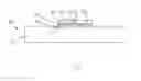
FIG. 1 is a cross-sectional view through a circuit board and connected die.
FIG. 2 shows a first embodiment interposer.
FIG. 3 shows a second embodiment interposer.
FIG. 4 shows a third embodiment interposer.
FIG. 5 shows a fourth embodiment interposer.
DETAILED DESCRIPTION OF THE PREFERRED EMBODIMENT
A printed circuit board assembly 20 is illustrated in FIG. 1 having a printed board 22 attached to a die 24. The die may be a field effect transistor, or some other type of solid state switch, and may provide a circuit breaker function to circuits on the printed board 22. Other switches and functions may also be used. The die 24 has a base of a first material along with circuit traces top and bottom, as known. The printed board 22 has a base of a second material, along with circuit traces. The particular disclosed embodiment has a silicon base die and a glass epoxy base printed board, but other materials may be utilized for the two members. The circuit traces are shown schematically at C and may be as known, to provide various functions.
The base materials for the die 24 and the printed board 22 are distinct, and have different coefficients of thermal expansion. As such, thermal stresses may exist at an interface between the two materials.
With the present application, a solder or other conductive material, such as a conductive adhesive is formed in one layer adjacent die 24, and another layer 28 adjacent the printed board 22. An intermediate material provides an interposer 30. Openings 32 within the material receive a conductive material to provide electrical connection between layers 26 and 28. The interposer 30 is selected to be of a material having a coefficient of thermal expansion intermediate that of the base materials of die 24 and the printed board 22. Thus, the thermal stresses between the die and printed board are reduced due to the interposer.
FIG. 2 shows a first embodiment interposer 130, wherein the layers 26 and 28 are connected by plated through holes 32 formed within the interposer material. The interposer material includes material 34, such that the thermal coefficient of expansion is intermediate that of the die 24 and the printed wiring board 22.
FIG. 3 shows another interposer embodiment 230 wherein a metal screen 232 is utilized. Solder or conductive adhesive flows through the openings 234 in the screen 232.
FIG. 4 shows another embodiment 330, wherein the interposer includes a material 332 formed with a plurality of holes 334. The holes are shown as round, but can be a plurality of shapes. Solder or conductive material flows through these openings to provide the electrical connections.
FIG. 5 shows another embodiment 50, wherein the printed board 52 is connected to the die 54 by an interposer 60. As shown, a conductive layer 58 is formed on the printed board 52, while a conductive layer 56 is provided adjacent the die 54. The interposer includes a back 62 in contact with the layer 56, and legs 60 which connect to the conductive portions 58 for the printed wiring board 52. The interposer itself is formed of a conductive metal to make the electrical connection. A space 66 is provided between the die 54 and the board 52 with this embodiment. This space can maximize the compliance between the printed wiring board 52 and the die 54. Other shapes can be utilized for the interposer.
The interposer can be made from any material having the coefficient of thermal expansion as mentioned above. One possible material would be a powdered metal injection molding compound. The process for forming materials from this compound could be optimized to obtain a specific coefficient of expansion. The porosity of this type material will allow the solder or other conductive type material to provide a superior electrical connection.
Another general type of material may be polyimide of bismuth telluride printed wiring board material. Again, an interposer would be plated on the top and bottom with plated through holes to provide an electrical connection between the top and bottom, such as shown for example in FIG. 2 above.
With all of the embodiments, it should be understood that the location of the conductive connection between the die and printed board, and through the interposer, is selected to provide appropriate electrical connections between the circuitry on the die and the printed board. The illustrations are a simplification of the actual likely connections.
Although embodiments of this invention have been disclosed, a worker of ordinary skill in this art would recognize that certain modifications would come within the scope of this invention. For that reason, the following claims should be studied to determine the true scope and content of this invention.
Claims
What is claimed is:1. A printed circuit board comprising:
a board having a substrate formed of a first material having a first coefficient of thermal expansion, and having circuit traces;
a die secured to said board, said die having circuit traces electrically connected to said board circuit traces, and said die having a base formed of a second material having a second coefficient of thermal expansion different than said first coefficient of thermal expansion; and
an interposer material positioned between said die and said board, said interposer having an electrical connection connecting said die circuit traces to said board circuit traces, said interposer being formed of a third material having a coefficient of thermal expansion intermediate said first and second coefficients of thermal expansion; and
wherein said interposer includes a base material with a plurality of openings, said openings receiving a conductive material to connect said die to said board.
2. The printed circuit board as set forth in claim 1, wherein said base material includes a solid plate having holes, with said conductive material extending through said holes to connect said die to said board.
3. The printed circuit board as set forth in claim 1, wherein said base material includes a metal screen, with openings in the screen allowing said conductive material to connect said die to said board.
4. The printed circuit board as set forth in claim 1, wherein said die is a switch.
5. The printed circuit board as set forth in claim 4, wherein said switch is a field effect transistor.
6. The printed circuit board as set forth in claim 1, wherein a first layer of conductive material is positioned between said interposer and said die, and a second layer of conductive material is positioned between said interposer and said board, with said connection extending through said interposer for connecting said first and second layers.
7. The printed circuit board as set forth in claim 6, wherein said first material is a glass filled epoxy.
8. The printed circuit board as set forth in claim 7, wherein said second material is silicon.
9. The printed circuit board as set forth in claim 1, wherein said interposer is formed of a powdered metal injection molding compound.
10. The printed circuit board as set forth in claim 1, wherein said interposer is formed of a polyimide of bismuth telluride.
11. A printed circuit board comprising:
a board having a substrate formed of a glass filled epoxy having a first coefficient of thermal expansion, said board having circuit traces;
a die secured to said board, said die having a base formed of a silicon having a second coefficient of thermal expansion, and said die being electrically connected to said board; and
an interposer material positioned between said die and said board, said interposer including a base material with a plurality of openings receiving a conductive material to provide an electrical connection between said die and said board.
12. The printed circuit board as set forth in claim 11, wherein said base material includes a solid plate having holes, with said conductive material extending through said holes.
13. The printed circuit board as set forth in claim 11, wherein said base material is provided by a metal screen, with openings in the screen allowing said conductive material to connect said die to said board.
14. The printed circuit board as set forth in claim 11, wherein a first layer of conductive material is positioned between said interposer and said die, and a second layer of conductive material is positioned between said interposer and said board, with said connection through said interposer connecting said first and second layers.
15. The printed circuit board as set forth in claim 11, wherein said die is a field effect transistor.
16. The printed circuit board as set forth in claim 11, wherein said interposer is formed of either a powdered metal injection molding compound and a polyimide of bismuth telluride.
17. The printed circuit board as set forth in claim 11, wherein said interposer has a coefficient of thermal expansion intermediate said first and second coefficients of thermal expansion.
18. The printed circuit board as set forth in claim 11, wherein each of said plurality of openings receives said conductive material.
Images & Drawings included:


Sources:
- United States Patent and Trademark Office - verify current appl. status at the USPTO↗
Recent applications in this class:
- » 20250120020 2025-04-10
SIGNAL TRACE TRANSITION FOR HIGH DATA RATE APPLICATIONS - » 20250081357 2025-03-06
INTERPOSER FOR TROUBLESHOOTING A BALL GRID ARRAY (BGA) DEVICE AND COUPLING THE BGA DEVICE TO A PRINTED CIRCUIT BOARD WITH LIMITED HEAT EXPOSURE - » 20250024608 2025-01-16
CIRCUIT STRUCTURE - » 20240414851 2024-12-12
PRINTED CIRCUIT BOARD FOR A REFLOW PROFILING PROCESS - » 20240324109 2024-09-26
SOLDER BARRIER CONTACT FOR AN INTEGRATED CIRCUIT - » 20240284603 2024-08-22
REMOVABLE LID FOR FLIP CHIP-BALL GRID ARRAY (FC-BGA) PACKAGES - » 20240244761 2024-07-18
PACKAGES WITH A SHORTEST DISTANCE BETWEEN PACKAGE CONNECTORS AND A SEATING PLANE OF AT LEAST 6 MILS - » 20230328895 2023-10-12
ELECTRONIC COMPONENT MOUNTING STRUCTURE AND METHOD FOR MANUFACTURING SAME - » 20230240020 2023-07-27
Integrated circuit device with edge bond dam - » 20230225060 2023-07-13
SOLDER PADS WITH CONCAVE EDGES FOR BALL GRID ARRAYS
Recent applications for this Assignee:
- » 20190097546 2019-03-28
Electric system architecture for a vehicle with multiple load characteristics - » 20130239578 2013-09-19
Internal thermal management for motor driven machinery - » 20130033038 2013-02-07
Starting/generating system with multi-functional circuit breaker - » 20120288372 2012-11-15
Teeter-restraint device for wind turbines - » 20120236439 2012-09-20
ELECTRICAL ACCUMULATOR UNITS WITH SAFE TURN-OFF - » 20110061447 2011-03-17
Biological agent detector method - » 20110005327 2011-01-13
In-situ monitoring device and method to determine accumulated printed wiring board vibration stress fatigue - » 20110005244 2011-01-13
Transcritical fluid cooling for aerospace applications - » 20110002786 2011-01-06
Remote pitch controller for a variable pitch propeller - » 20100327820 2010-12-30
Active damping for synchronous generator torsional oscillations