Semiconductor device comprising a passive component of capacitors and process for fabrication
US20120025348A1
2012-02-02
13/179,640
2011-07-11
✅ Patent granted
US 9,029,928 B2
2015-05-12
-
-
Mohsen Ahmadi
Gardere Wynne Sewell LLP
2032-12-03
Abstract:
A semiconductor device includes a wafer having a frontside and a backside. The wafer is formed from at least one integrated circuit chip having an electrical connection frontside co-planar with the wafer frontside and a backside co-planar with the wafer backside. A passive component including at least one conductive plate and a dielectric plate is positioned adjacent the integrated circuit chip. An encapsulation block embeds the integrated circuit chip and the passive component, the block having a frontside co-planar with the wafer frontside and a backside co-planar with the wafer backside. An electrical connection is made between the electrical connection frontside and the passive component. That electrical connection includes connection lines placed on the wafer frontside and wafer backside. The electrical connection further includes at least one via passing through the encapsulation block.
Inventors:
- Romain Coffy 20 🇫🇷 Saint Martin Le Vinoux, France
- Yvon Imbs 12 🇫🇷 Quaix En Chartreuse, France
- Laurent Marechal 4 🇫🇷 Grenoble, France
Assignee:
- STMICROELECTRONICS (GRENOBLE 2) SAS 704 🇫🇷 Grenoble, France
- STMicroelectronics (Grenoble) SAS 50 🇫🇷 Grenoble, France
Applicant:
Interested in similar patents?
Get notified when new applications in this technology area are published.
Classification:
H01L24/19 » CPC further
Arrangements for connecting or disconnecting semiconductor or solid-state bodies; Methods or apparatus related thereto; Means for bonding being attached to, or being formed on, the surface to be connected, e.g. chip-to-package, die-attach, "first-level" interconnects; Manufacturing methods related thereto; High density interconnect [HDI] connectors; Manufacturing methods related thereto Manufacturing methods of high density interconnect preforms
H01L21/568 » CPC further
Processes or apparatus adapted for the manufacture or treatment of semiconductor or solid state devices or of parts thereof; Manufacture or treatment of semiconductor devices or of parts thereof the devices having at least one potential-jump barrier or surface barrier, e.g. PN junction, depletion layer or carrier concentration layer; Assembly of semiconductor devices using processes or apparatus not provided for in a single one of the subgroups - , e.g. sealing of a cap to a base of a container; Encapsulations, e.g. encapsulation layers, coatings Temporary substrate used as encapsulation process aid
H01L2224/04105 » CPC further
Indexing scheme for arrangements for connecting or disconnecting semiconductor or solid-state bodies and methods related thereto as covered by; Means for bonding being attached to, or being formed on, the surface to be connected, e.g. chip-to-package, die-attach, "first-level" interconnects; Manufacturing methods related thereto; Bonding areas; Manufacturing methods related thereto; Structure, shape, material or disposition of the bonding areas prior to the connecting process Bonding areas formed on an encapsulation of the semiconductor or solid-state body, e.g. bonding areas on chip-scale packages
H01L2224/12105 » CPC further
Indexing scheme for arrangements for connecting or disconnecting semiconductor or solid-state bodies and methods related thereto as covered by; Means for bonding being attached to, or being formed on, the surface to be connected, e.g. chip-to-package, die-attach, "first-level" interconnects; Manufacturing methods related thereto; Bump connectors; Manufacturing methods related thereto; Structure, shape, material or disposition of the bump connectors prior to the connecting process Bump connectors formed on an encapsulation of the semiconductor or solid-state body, e.g. bumps on chip-scale packages
H01L2224/73267 » CPC further
Indexing scheme for arrangements for connecting or disconnecting semiconductor or solid-state bodies and methods related thereto as covered by; Means for bonding being of different types provided for in two or more of groups; Location after the connecting process on different surfaces Layer and HDI connectors
H01L2224/9222 » CPC further
Indexing scheme for arrangements for connecting or disconnecting semiconductor or solid-state bodies and methods related thereto as covered by; Methods for connecting semiconductor or solid state bodies including different methods provided for in two or more of groups - ; Specific sequence of method steps; Connecting different surfaces of the semiconductor or solid-state body with connectors of different types Sequential connecting processes
H01L2924/18162 » CPC further
Indexing scheme for arrangements or methods for connecting or disconnecting semiconductor or solid-state bodies as covered by; Details of package parts other than the semiconductor or other solid state devices to be connected; Encapsulation; Shape; Exposing the passive side of the semiconductor or solid-state body of a chip with build-up interconnect
H01L2924/19105 » CPC further
Indexing scheme for arrangements or methods for connecting or disconnecting semiconductor or solid-state bodies as covered by; Details of hybrid assemblies other than the semiconductor or other solid state devices to be connected; Disposition of discrete passive components in a side-by-side arrangement on a common die mounting substrate
H01L2224/82 » CPC further
Indexing scheme for arrangements for connecting or disconnecting semiconductor or solid-state bodies and methods related thereto as covered by; Methods for connecting semiconductor or other solid state bodies using means for bonding being attached to, or being formed on, the surface to be connected by forming build-up interconnects at chip-level, e.g. for high density interconnects [HDI]
H01L2924/14 » CPC further
Indexing scheme for arrangements or methods for connecting or disconnecting semiconductor or solid-state bodies as covered by; Details of semiconductor or other solid state devices to be connected; Device type Integrated circuits
H01L2924/00 » CPC further
Indexing scheme for arrangements or methods for connecting or disconnecting semiconductor or solid-state bodies as covered by
H01L23/28 IPC
Details of semiconductor or other solid state devices Encapsulations, e.g. encapsulating layers, coatings, e.g. for protection
H01L29/92 IPC
Semiconductor devices adapted for rectifying, amplifying, oscillating or switching, or capacitors or resistors with at least one potential-jump barrier or surface barrier, e.g. PN junction depletion layer or carrier concentration layer; Details of semiconductor bodies or of electrodes thereof; Multistep manufacturing processes therefor; Types of semiconductor device ; Multistep manufacturing processes therefor controllable only by variation of the electric current supplied, or only the electric potential applied, to one or more of the electrodes carrying the current to be rectified, amplified, oscillated or switched Capacitors with potential-jump barrier or surface barrier
H01L23/5389 » CPC further
Details of semiconductor or other solid state devices; Arrangements for conducting electric current within the device in operation from one component to another, i.e. interconnections, e.g. wires, lead frames the interconnection structure between a plurality of semiconductor chips being formed on, or in, insulating substrates the chips being integrally enclosed by the interconnect and support structures
H01L24/18 » CPC further
Arrangements for connecting or disconnecting semiconductor or solid-state bodies; Methods or apparatus related thereto; Means for bonding being attached to, or being formed on, the surface to be connected, e.g. chip-to-package, die-attach, "first-level" interconnects; Manufacturing methods related thereto High density interconnect [HDI] connectors; Manufacturing methods related thereto
H01L23/5383 » CPC further
Details of semiconductor or other solid state devices; Arrangements for conducting electric current within the device in operation from one component to another, i.e. interconnections, e.g. wires, lead frames the interconnection structure between a plurality of semiconductor chips being formed on, or in, insulating substrates Multilayer substrates
H01L24/82 » CPC further
Arrangements for connecting or disconnecting semiconductor or solid-state bodies; Methods or apparatus related thereto; Methods for connecting semiconductor or other solid state bodies using means for bonding being attached to, or being formed on, the surface to be connected by forming build-up interconnects at chip-level, e.g. for high density interconnects [HDI]
H01L24/96 » CPC further
Arrangements for connecting or disconnecting semiconductor or solid-state bodies; Methods or apparatus related thereto; Batch processes at chip-level, i.e. with connecting carried out on a plurality of singulated devices, i.e. on diced chips the devices being encapsulated in a common layer, e.g. neo-wafer or pseudo-wafer, said common layer being separable into individual assemblies after connecting
H01L24/97 » CPC further
Arrangements for connecting or disconnecting semiconductor or solid-state bodies; Methods or apparatus related thereto; Batch processes at chip-level, i.e. with connecting carried out on a plurality of singulated devices, i.e. on diced chips the devices being connected to a common substrate, e.g. interposer, said common substrate being separable into individual assemblies after connecting
H01L2224/18 » CPC further
Indexing scheme for arrangements for connecting or disconnecting semiconductor or solid-state bodies and methods related thereto as covered by; Means for bonding being attached to, or being formed on, the surface to be connected, e.g. chip-to-package, die-attach, "first-level" interconnects; Manufacturing methods related thereto High density interconnect [HDI] connectors; Manufacturing methods related thereto
H01L2224/97 » CPC further
Indexing scheme for arrangements for connecting or disconnecting semiconductor or solid-state bodies and methods related thereto as covered by; Batch processes at chip-level, i.e. with connecting carried out on a plurality of singulated devices, i.e. on diced chips the devices being connected to a common substrate, e.g. interposer, said common substrate being separable into individual assemblies after connecting
H05K1/185 » CPC further
Printed circuits; Printed circuits structurally associated with non-printed electric components associated with components mounted in the printed circuit board, e.g. insert mounted components [IMC] Components encapsulated in the insulating substrate of the printed circuit or incorporated in internal layers of a multilayer circuit
H01L2924/01058 » CPC further
Indexing scheme for arrangements or methods for connecting or disconnecting semiconductor or solid-state bodies as covered by; Chemical elements Cerium [Ce]
H01L2924/15311 » CPC further
Indexing scheme for arrangements or methods for connecting or disconnecting semiconductor or solid-state bodies as covered by; Details of package parts other than the semiconductor or other solid state devices to be connected; Die mounting substrate; Connection portion the connection portion being formed only on the surface of the substrate opposite to the die mounting surface being a ball array, e.g. BGA
H05K2201/10015 » CPC further
Indexing scheme relating to printed circuits covered by; Details of components or other objects attached to or integrated in a printed circuit board; Types of components Non-printed capacitor
H05K2201/10015 » CPC further
Indexing scheme relating to printed circuits covered by; Details of components or other objects attached to or integrated in a printed circuit board; Types of components Non-printed capacitor
H05K2201/10674 » CPC further
Indexing scheme relating to printed circuits covered by; Details of components or other objects attached to or integrated in a printed circuit board; Details of electrical connections of non-printed components, e.g. special leads; Components characterised by their electrical contacts Flip chip
H05K2203/1469 » CPC further
Indexing scheme relating to apparatus or processes for manufacturing printed circuits covered by; Related to the order of processing steps; Applying or finishing the circuit pattern after another process, e.g. after filling of vias with conductive paste, after making printed resistors Circuit made after mounting or encapsulation of the components
H01L2924/01033 » CPC further
Indexing scheme for arrangements or methods for connecting or disconnecting semiconductor or solid-state bodies as covered by; Chemical elements Arsenic [As]
H01L23/642 » CPC further
Details of semiconductor or other solid state devices; Structural electrical arrangements for semiconductor devices not otherwise provided for, e.g. in combination with batteries; Impedance arrangements Capacitive arrangements
H01L25/16 » CPC further
Assemblies consisting of a plurality of individual semiconductor or other solid state devices ; Multistep manufacturing processes thereof the devices being of types provided for in two or more different main groups of - , e.g. forming hybrid circuits
H01L27/108 IPC
Devices consisting of a plurality of semiconductor or other solid-state components formed in or on a common substrate including semiconductor components specially adapted for rectifying, oscillating, amplifying or switching and having at least one potential-jump barrier or surface barrier; including integrated passive circuit elements with at least one potential-jump barrier or surface barrier the substrate being a semiconductor body including a plurality of individual components in a repetitive configuration including field-effect components Dynamic random access memory structures
H01L29/94 IPC
Semiconductor devices adapted for rectifying, amplifying, oscillating or switching, or capacitors or resistors with at least one potential-jump barrier or surface barrier, e.g. PN junction depletion layer or carrier concentration layer; Details of semiconductor bodies or of electrodes thereof; Multistep manufacturing processes therefor; Types of semiconductor device ; Multistep manufacturing processes therefor controllable only by variation of the electric current supplied, or only the electric potential applied, to one or more of the electrodes carrying the current to be rectified, amplified, oscillated or switched; Capacitors with potential-jump barrier or surface barrier Metal-insulator-semiconductors, e.g. MOS
H01L29/40 IPC
Semiconductor devices adapted for rectifying, amplifying, oscillating or switching, or capacitors or resistors with at least one potential-jump barrier or surface barrier, e.g. PN junction depletion layer or carrier concentration layer; Details of semiconductor bodies or of electrodes thereof; Multistep manufacturing processes therefor Electrodes ; Multistep manufacturing processes therefor
H01L23/12 IPC
Details of semiconductor or other solid state devices Mountings, e.g. non-detachable insulating substrates
H01L23/053 IPC
Details of semiconductor or other solid state devices; Containers; Seals characterised by the shape of the container or parts, e.g. caps, walls the container being a hollow construction and having an insulating or insulated base as a mounting for the semiconductor body
H01L21/56 » CPC main
Processes or apparatus adapted for the manufacture or treatment of semiconductor or solid state devices or of parts thereof; Manufacture or treatment of semiconductor devices or of parts thereof the devices having at least one potential-jump barrier or surface barrier, e.g. PN junction, depletion layer or carrier concentration layer; Assembly of semiconductor devices using processes or apparatus not provided for in a single one of the subgroups - , e.g. sealing of a cap to a base of a container Encapsulations, e.g. encapsulation layers, coatings
H01L23/00 IPC
Details of semiconductor or other solid state devices
H01L23/64 IPC
Details of semiconductor or other solid state devices; Structural electrical arrangements for semiconductor devices not otherwise provided for, e.g. in combination with batteries Impedance arrangements
H01L23/538 IPC
Details of semiconductor or other solid state devices; Arrangements for conducting electric current within the device in operation from one component to another, i.e. interconnections, e.g. wires, lead frames the interconnection structure between a plurality of semiconductor chips being formed on, or in, insulating substrates
H05K1/18 IPC
Printed circuits Printed circuits structurally associated with non-printed electric components
H05K1/18 IPC
Printed circuits Printed circuits structurally associated with non-printed electric components
Description
PRIORITY CLAIM
This application claims priority from French Application for Patent No. 1056159 filed Jul. 27, 2010, the disclosure of which is hereby incorporated by reference.
TECHNICAL FIELD
The present invention relates to the field of semiconductor devices.
BACKGROUND
It is known to produce reconstituted wafers comprising, in locations, integrated circuit chips embedded in an encapsulation material and to saw these wafers so as to form individual semiconductor devices.
Nevertheless, it is not possible at the present time to integrate into the wafers, near the chips, capacitors such as those currently used, especially due to their shape and their electrical connection means.
SUMMARY
A process for fabricating a semiconductor device is provided.
This process comprises: placing, in at least one location on a receiving surface of a carrier, an electrical connection frontside of at least one integrated circuit chip and a frontside of at least one passive component comprising conductive plates separated by dielectric plates forming capacitors; forming on said receiving surface a layer of an encapsulation material so as to obtain, in said location, a wafer comprising an encapsulation block in which the chip and the passive component are embedded and having a frontside comprising the frontside of the chip and the frontside of the passive component; then selectively connecting at least some of said conductive plates to the chip, so that at least some of the capacitors are connected to the chip.
It is thus possible to prefabricate a passive component having a simple structure, to integrate it into the encapsulation block, and then to form one or more capacitors, as required, when electrical connections are made to the chip.
The process may comprise: forming at least one front electrical connection track on the frontside of the wafer.
The process may comprise: forming at least one back electrical connection track on the backside of the wafer, an electrical connection via through the wafer and a front electrical connection track on the frontside of the wafer, the back track and the front track being connected by the electrical connection via.
The process may comprise: placing the passive component such that said plates extend perpendicularly to said receiving surface, then selectively connecting at least some of the lands of said conductive plates to the chip.
The process may comprise: placing the passive component such that said plates extend parallel to said receiving surface.
The process may comprise: placing a passive component having a dielectric plate on the receiving surface, then forming at least one additional conductive plate on the frontside of this dielectric plate so as to form a capacitor comprising this conductive plate and the adjacent conductive plate of the passive component, which are separated by this first dielectric plate.
A semiconductor device is also provided, which comprises a wafer having a frontside and comprising at least one integrated circuit chip having an electrical connection frontside, at least one passive component having a frontside and comprising conductive plates separated by dielectric plates, forming capacitors, and an encapsulation block in which the integrated circuit chip and the passive component are embedded, a frontside of the encapsulation block, the frontside of the integrated circuit chip and the frontside of the passive component forming the frontside of the wafer; and electrical connection means connecting at least some of said conductive plates and the integrated circuit chip, these electrical connection means being formed on the frontside of the wafer and/or on the backside of the wafer, through the encapsulation block and on the frontside of the wafer.
The passive component may comprise plates which extend perpendicularly to the frontside of the wafer, the electrical connection means being connected to the lands of the conductive plates.
Said plates may extend through the thickness of the wafer.
The passive component may comprise plates which extend parallel to the frontside of the wafer.
The passive component may comprise a dielectric plate adjacent to the frontside of the wafer, at least one conductive plate being formed on the frontside of this dielectric plate.
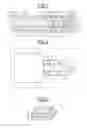
BRIEF DESCRIPTION OF THE DRAWINGS
Semiconductor devices will now be described by way of non-limiting example, illustrated by the drawings in which:
FIG. 1 shows a cross section of a semiconductor device;
FIG. 2 shows a front view of the semiconductor device in FIG. 1, without a surface layer;
FIG. 3 shows a perspective view of a passive component of the semiconductor device in FIG. 1;
FIG. 4 shows the semiconductor device in FIG. 1, according to one fabrication step;
FIG. 5 shows the semiconductor device in FIG. 1, according to another fabrication step;
FIG. 6 shows the semiconductor device in FIG. 1, according to another fabrication step;
FIG. 7 shows the semiconductor device in FIG. 1, according to another fabrication step;
FIG. 8 shows a cross section of another semiconductor device;
FIG. 9 shows a front view of the semiconductor device in FIG. 8, without a surface layer;
FIG. 10 shows a perspective view of a passive component of the semiconductor device in FIG. 8;
FIG. 11 shows the semiconductor device in FIG. 8, according to one fabrication step;
FIG. 12 shows the semiconductor device in FIG. 8, according to another fabrication step;
FIG. 13 shows the semiconductor device in FIG. 8, according to another fabrication step; and
FIG. 14 shows the semiconductor device in FIG. 8, according to another fabrication step.
DETAILED DESCRIPTION OF THE DRAWINGS
A semiconductor device 1 illustrated in FIGS. 1 to 3 comprises a wafer 2 which has a frontside 3 and a backside 4, in parallel.
The wafer 2 comprises a block of a dielectric encapsulation material 5 in which a prefabricated integrated circuit chip 6 and a prefabricated passive component 7 are embedded, these being placed so that a frontside 8 of the chip 6, in which the integrated circuits are formed and which has electrical connection pads, a frontside 9 of the passive component 7 and a frontside 10 of the encapsulation block 5 are in the same plane forming the frontside 3 of the wafer 2, the passive component 7 being placed at a distance to the side of the chip 6. Thus, the frontside 8 of the chip 6 and the frontside 9 of the passive component 7 are not covered by the encapsulation block 5.
The passive component 7 comprises a plurality of superposed plates, which are placed parallel to the frontside 3 of the wafer 2. According to the example shown, the passive component 7 comprises in succession, in the thickness direction of the wafer 2, a dielectric plate 11 having the aforementioned side 9, a conductive plate 12, a dielectric plate 13 and a conductive plate 14, the conductive plates 12 and 14 being for example metallic. The plate 12 completely covers the plate 11, the plate 13 does not completely cover the plate 12 and the plate 14 completely covers the plate 13, the conductive plate 14 being, in the example shown, distant from the backside 4 of the wafer 2.
On the frontside 3 of the wafer 2, two conductive front plates 15 and 16 are formed, which are connected to electrical connection pads on the frontside 8 of the chip 6 by front electrical connection tracks 17 and 18, the conductive plates 15 and 16 being located on the frontside 9 of the dielectric plate 11 and being distant from each other. The conductive front plates 15 and 16 have the same thickness as the front electrical connection tracks 17 and 18.
Behind the plates 12 and 14, and between these plates 12 and 14 and the backside 4 of the wafer 2, holes 19 and 20 are provided in the encapsulation block 5, which are filled with a conductive material so as to form electrical connection vias 21 and 22.
According to one variant, the passive component 7 could have the same thickness as the wafer 2. In this case, the electrical connection via 22 could be omitted.
To the side of the chip 6 and the passive component 7, and between the frontside 3 and the backside 4 of the wafer 2, through-holes 23 and 24 are provided in the encapsulation block 5 and are filled with a conductive material so as to form electrical connection vias 25 and 26.
On the frontside 3 of the wafer 2, front electrical connection tracks 27 and 28 are formed connecting the vias 25 and 26, respectively, to electrical connection pads on the frontside 8 of the chip 6 and, on the backside 4 of the wafer 2, back electrical connection tracks 29 and 30 are formed connecting the vias 21 and 22 to the vias 25 and 26, respectively.
Thus, the passive component 7 defines three capacitors connected to the chip 6, namely a first capacitor C1 comprising the conductive plate 12 and the conductive plate 15 which are separated by the dielectric plate 11, a second capacitor C2 comprising the conductive plate 12 and the conductive plate 16 which are separated by the dielectric plate 11, and a third capacitor C3 comprising the conductive plates 12 and 14 which are separated by the dielectric plate 13.
On the frontside 3 of the wafer 2, and covering the conductive plates 15 and 16 and the electrical connection tracks 17, 18, 27 and 28, a dielectric layer 31 is provided, incorporating an electrical connection network 32 allowing electrical connection pads, on the frontside 8 of the chip 6, and external electrical connection bumps 33, placed on a frontside of the layer 31, to be selectively connected.
A protective dielectric layer 34 is provided on the backside 4 of the wafer 2, covering the electrical connection tracks 29 and 30.
The semiconductor device 1 may be produced in the following way, by suitably employing means used in the microelectronics field.
As illustrated in FIG. 4, in respective adjacent, for example square, locations 35 in a receiving surface 36 of a carrier 37, chips 6 and passive components 7 are placed, their frontsides 8 and 9 being placed against the receiving surface 36, the receiving surface 36 being for example self-adhesive.
As illustrated in FIG. 5, an encapsulation layer 38 is formed on the receiving surface 36 of the carrier 37, embedding the chips 6 and the passive components 7 and this layer 38 is then leveled or thinned, for example as far as the backside of the chips 6, so as to obtain a large reconstituted wafer 39 forming, respectively in the locations 35, encapsulation blocks 5 holding chips 6 and passive components 7.
Then, as illustrated in FIG. 6, holes 19, 20, 23 and 24 are produced, respectively in the locations 35, in the encapsulation layer 38 and these holes are filled with a conductive material so as to form vias 21, 22, 25 and 26, respectively, in the encapsulation blocks 5.
Then, as partially illustrated in FIG. 7 and more fully shown in FIG. 1, the layer 31 is produced on the frontside 3 of the wafer 2, incorporating therein, respectively in the locations 35, and on the same metallization level, the conductive plates 15 and 16, the front electrical connection tracks 17, 18, 27 and 28 and the electrical connection network 32. An intermediate dielectric layer could be formed directly on the frontside of the wafer 2, the conductive plates 15 and 16, the front electrical connection tracks 17, 18, 27 and 28 and the electrical connection network 32 then being produced on this intermediate dielectric layer and passing through the latter in places where electrical connection is required. Moreover, the electrical connection network 32 could nevertheless comprise several metallic levels.
Then, on the backside 4 of the wafer 2, the layer 34 is produced, incorporating therein, in the locations 35 respectively, and on the same metallization level, the back electrical connection tracks 29 and 30.
Then, the electrical connection bumps 33 are placed on the front layer 31.
Finally, the large wafer 39 obtained is singulated, along the edges of the locations 35, for example by sawing, so as to obtain a plurality of semiconductor devices 1.
It follows from the above that when the conductive front plates 15 and 16 are produced, at the same time as the front electrical connection tracks 17 and 18, the capacitances of the capacitors C1 and C2 are defined, especially by choosing the areas of these plates 15 and 16. Of course, one or more capacitors could be produced by forming one or more conductive plates on the frontside 3, at the same time as one or more tracks for electrical connection to the chip 6.
In addition, being provided with a prefabricated passive component comprising several capacitors, only some of the capacitors could be connected, as a function of the chip 6 used and of the requirements related to the operation and applications of the latter.
Another semiconductor device 50, illustrated in FIGS. 8 to 10, comprises a wafer 51 which has a frontside 52 and a backside 53, in parallel.
The wafer 51 comprises a block of an encapsulation material 54 in which a prefabricated integrated circuit chip 55 and a prefabricated passive component 56 are embedded, these being placed so that an electrical connection frontside 57 of the chip 55, a frontside 58 of the passive component 56, and a frontside 59 of the encapsulation block 5 are in the same plane formed by the frontside 52 of the wafer 51, the passive component 56 being placed at a distance to the side of the chip 55.
The passive component 56 comprises a plurality of superposed plates, placed perpendicular to the frontside 52 of the wafer 51. According to the example shown, the passive component 56 comprises four parallel, for example metallic, conductive plates 60, 61, 62 and 63, separated by three dielectric plates 64, 65 and 66, so as to form three capacitors C10, C11 and C12.
The conductive plates 60-63 and the dielectric plates 64-66 are placed so as to have front lands which form the side 58 of the passive component 56 in the plane of the frontside 57 of the wafer 51, and opposite back lands which are in the plane of the backside 53 of the wafer 51, the conductive plates 60-63 and the dielectric plates 64-66 consequently having, between these opposite lands, a width corresponding to the thickness of the wafer 51.
By way of example, the capacitors C10-C12 may be connected to the chip 55 in the following way.
For example, front electrical connection tracks 67, 68 and 69 may be formed on the frontside 52 of the wafer 51 so as to connect the front lands of the conductive plates 60, 61 and 62 to front pads of the chip 55, by extending onto these front lands and onto these pads, so that the capacitors C10 and C11 are connected to the chip 55 by the front tracks 67 and 68 and by the front tracks 68 and 69, respectively.
Furthermore, the encapsulation block 54 may have a through-hole 70 filled with a material forming an electrical connection via 71, a front electrical connection track 72 possibly being formed on the frontside 52 of the wafer 51 so as to connect the via 71 and a front pad of the chip 55, by extending over this via and this pad, and a back electrical connection track 73 possibly being formed on the backside 53 of the wafer 51 so as to connect the via 71 and the back land of the conductive plate 63, by extending over this via and this land, so that the capacitor C12 is connected to the chip 55 by the via 71, the front electrical connection track 72 and the back electrical connection track 73.
On the frontside 52 of the wafer 51, and covering the frontside of the passive component 56 and the front electrical connection tracks 67-69 and 72, a dielectric layer 74 is provided, incorporating an electrical connection network 75 allowing electrical connection pads, on the frontside 57 of the chip 55, and external electrical connection bumps 76, placed on a frontside of the layer 74, to be selectively connected.
A protective dielectric layer 77 is provided on the backside 53 of the wafer 51, covering the backside of the passive component 56 and the back electrical connection track 73.
The semiconductor device 50 may be produced in the following way.
As illustrated in FIG. 11, in respective adjacent, for example square, locations 78 in a receiving surface 79 of a carrier 80, chips 55 and passive components 56 are placed, their frontsides 57 and 58 being placed against the receiving surface 79, the receiving surface 79 being for example self-adhesive.
As illustrated in FIG. 12, an encapsulation layer 81 is formed on the receiving surface 79 of the carrier 80, embedding the chips 55 and the passive components 56 and this layer 81 is then leveled or thinned, until the backsides of the passive components 56 are exposed, so as to obtain a large reconstituted wafer 82 forming, respectively in the locations 78, encapsulation blocks 54 holding chips 55 and passive components 56.
Then, as illustrated in FIG. 13, a hole 70 is produced, respectively in the locations 78, in the encapsulation layer 81 and this hole 70 is filled with a conductive material so as to form the via 71, respectively, in the encapsulation blocks 54.
Then, as partially illustrated in FIG. 14 and more fully shown in FIG. 8, and in a way equivalent to that described above, with reference to FIGS. 1 and 7, in relation to the device 1, on the one hand, front electrical connection tracks 67, 68, 69 and 72 and the network 75 are produced, respectively in the locations 78, in the dielectric front layer 74 and, on the other hand, the back electrical connection track 73 is produced in the dielectric back layer 77.
Then the bumps 76 are placed in each location 78
Finally, the large wafer 82 obtained is singulated, along the edges of the locations 78, for example by sawing, so as to obtain a plurality of semiconductor devices 50.
In the two examples just described, being provided with a prefabricated passive component comprising several capacitors, only some of the capacitors could be connected, as a function of the chip 55 used and of the requirements related to the operation and applications of the latter.
According to a variant embodiment, a semiconductor device could comprise a passive component some of the capacitors of which would be connected in series or in parallel, so as to create a resultant capacitor connected to the chip.
According to a variant embodiment, a semiconductor device could comprise a passive component at least one of the capacitors of which would be directly connected to one of the external electrical connection bumps.
According to a variant embodiment, a semiconductor device could comprise a passive component at least one of the capacitors of which would be directly connected to another semiconductor device, for example stacked on its backside.
The present invention is not limited to the examples described above. Many other variant embodiments are possible without departing from the scope defined by the appended claims.
Claims
What is claimed is:1. A process for fabricating a semiconductor device, comprising:
placing, in at least one location on a receiving surface of a carrier, an electrical connection frontside of at least one integrated circuit chip and a frontside of at least one passive component comprising at least one conductive plate and a dielectric plate for forming a capacitor;
forming on said receiving surface a layer of an encapsulation material so as to obtain, in said location, a wafer comprising an encapsulation block in which the chip and the passive component are embedded and having a frontside comprising the frontside of the chip and the frontside of the passive component;
then selectively connecting said at least one conductive plate to the chip, so that said capacitor is connected to the chip.
2. The process according to claim 1, comprising: forming at least one front electrical connection track on the frontside of the wafer.
3. The process according to claim 2, comprising: forming at least one back electrical connection track on the backside of the wafer, and forming an electrical connection via through the wafer and forming a front electrical connection track on the frontside of the wafer, the back track and the front track being connected by the electrical connection via.
4. The process according to claim 1, comprising: placing the passive component such that said at least one conductive plate extends perpendicular to said receiving surface, then selectively connecting an edge of said at least one conductive plate to the chip.
5. The process according to claim 1, comprising: placing the passive component such that said at least one plate extends parallel to said receiving surface.
6. The process according to claim 5, comprising: placing the passive component having a dielectric plate on the receiving surface, then forming at least one additional conductive plate on the frontside of this dielectric plate so as to form said capacitor comprising the additional conductive plate and the at least one conductive plate, which are separated by the first dielectric plate.
7. A semiconductor device, comprising:
a wafer having a frontside and comprising at least one integrated circuit chip having an electrical connection frontside, at least one passive component having a frontside and comprising at least one conductive plate and a dielectric plate for forming a capacitor, the wafer including an encapsulation block in which the integrated circuit chip and the passive component are embedded, a frontside of the encapsulation block, the frontside of the integrated circuit chip and the frontside of the passive component forming the frontside of the wafer; and
electrical connections configured to connect at least some of said conductive plates and the integrated circuit chip, these electrical connections being formed on the frontside of the wafer and/or on the backside of the wafer, through the encapsulation block and on the frontside of the wafer.
8. The device according to claim 7, in which the passive component comprises said at least one conductive plate which extends perpendicularly to the frontside of the wafer, the electrical connections being connected to an edge of the conductive plate.
9. The device according to claim 8, in which said at least one conductive plate extends through the thickness of the wafer.
10. The device according to claim 7, in which the passive component comprises said at least one conductive plate which extends parallel to the frontside of the wafer.
11. The device according to claim 10, in which the passive component comprises a dielectric plate adjacent to the frontside (3) of the wafer, and further comprising an additional conductive plate being formed on the frontside of this dielectric plate.
12. A process, comprising:
placing an electrical connection frontside of an integrated circuit chip on a receiving surface of a carrier;
placing a capacitive structure comprising at least one conductive plate and at least one dielectric plate on the receiving surface of the carrier adjacent to the integrated circuit chip;
providing an encapsulating material layer surrounding the integrated circuit chip and the capacitive structure, the encapsulating material layer having a backside co-planar with a backside of the integrated circuit chip;
forming an electrical connection between the electrical connection frontside of the integrated circuit chip and the at least one conductive plate of the capacitive structure, said electrical connection comprising a via passing through the encapsulating material layer and a connection line formed on the backside of the encapsulating material layer.
13. The process of claim 12, wherein placing the capacitive structure comprises orienting the at least one conductive plate parallel to the receiving surface of the carrier.
14. The process of claim 13 wherein forming the electrical connection further comprises another via passing through the encapsulating material layer between the connection line formed on the backside of the encapsulating material layer and the at least one conductive plate.
15. The process of claim 14, further comprising:
removing said carrier, the electrical connection frontside of the integrated circuit chip being co-planar with a frontside of the encapsulating material layer;
forming another conductive plate and another electrical connection between the electrical connection frontside of the integrated circuit chip and the another conductive plate, said another electrical connection comprising a connection line formed on the frontside of the encapsulating material layer.
16. The process of claim 12, wherein placing the capacitive structure comprises orienting the at least one conductive plate perpendicular to the receiving surface of the carrier.
17. The process of claim 16 wherein forming the electrical connection further comprises making an electrical connection between the connection line formed on the backside of the encapsulating material layer and an edge of the at least one conductive plate.
18. The process of claim 17, wherein the capacitive structure comprises an another conductive plate oriented perpendicular to the receiving surface of the carrier, further comprising:
removing said carrier, the electrical connection frontside of the integrated circuit chip being co-planar with a frontside of the encapsulating material layer;
forming another electrical connection between the electrical connection frontside of the integrated circuit chip and the another conductive plate, said another electrical connection comprising a connection line formed on the frontside of the encapsulating material layer.
19. The process of claim 18 wherein forming the another electrical connection further comprises making an electrical connection between the connection line formed on the frontside of the encapsulating material layer and an edge of the another conductive plate.
20. A semiconductor device, comprising:
an integrated circuit chip having an electrical connection frontside and a backside;
a capacitive structure comprising at least one conductive plate and at least one dielectric plate;
an encapsulating material layer surrounding the integrated circuit chip and capacitive structure, the encapsulating material layer having a frontside co-planar with the electrical connection frontside of the integrated circuit chip and a backside co-planar with the backside of the integrated circuit chip; and
an electrical connection between the electrical connection frontside of the integrated circuit chip and the at least one conductive plate of the capacitive structure, said electrical connection comprising a via passing through the encapsulating material layer and a connection line formed on the backside of the encapsulating material layer.
21. The device of claim 20, wherein the at least one conductive plate is oriented parallel to the frontside and backside of the encapsulating material layer.
22. The device of claim 21 wherein said electrical connection between the electrical connection frontside of the integrated circuit chip and the at least one conductive plate of the capacitive structure comprises another via passing through the encapsulating material layer between the connection line formed on the backside of the encapsulating material layer and the at least one conductive plate.
23. The device of claim 22, wherein the capacitive structure further comprises another conductive plate, further comprising another electrical connection between the electrical connection frontside of the integrated circuit chip and the another conductive plate, said another electrical connection comprising a connection line formed on the frontside of the encapsulating material layer.
24. The device of claim 20, wherein the at least one conductive plate is oriented parallel to the frontside and backside of the encapsulating material layer.
25. The device of claim 24 wherein the connection line formed on the backside of the encapsulating material layer is connected to an edge of the at least one conductive plate.
26. The device of claim 25, wherein the capacitive structure comprises an another conductive plate oriented perpendicular to the receiving surface of the carrier, further comprising:
another electrical connection between the electrical connection frontside of the integrated circuit chip and the another conductive plate, said another electrical connection comprising a connection line formed on the frontside of the encapsulating material layer.
27. The device of claim 26 wherein the connection line formed on the frontside of the encapsulating material layer is connected to an edge of the another conductive plate.
Images & Drawings included:


Sources:
- United States Patent and Trademark Office - verify current appl. status at the USPTO↗
Similar patent applications:
Recent applications in this class:
- » 20250293050 2025-09-18
WAFER PROCESSING METHOD AND WAFER PROCESSING APPARATUS - » 20250273481 2025-08-28
METHOD OF MANUFACTURING SEMICONDUCTOR DEVICES AND CORRESPONDING DEVICE - » 20250210375 2025-06-26
SURFACE TREATMENT COMPOSITION AND METHOD FOR PRODUCING WAFER - » 20250191939 2025-06-12
SEMICONDUCTOR DEVICES AND METHODS OF MANUFACTURING - » 20250191938 2025-06-12
Overmolding Structures in Glass - » 20250149346 2025-05-08
METHOD OF FORMING ELECTROMAGNETIC-WAVE SHIELD, METHOD OF MANUFACTURING STRUCTURE, AND STRUCTURE - » 20250096008 2025-03-20
PACKAGED SEMICONDUCTOR DEVICES AND METHODS OF PACKAGING SEMICONDUCTOR DEVICES - » 20250062137 2025-02-20
POWER SEMICONDUCTOR MODULE ARRANGEMENT AND METHOD FOR PRODUCING THE SAME - » 20250062136 2025-02-20
Packages with Implantation - » 20250014912 2025-01-09
METHOD FOR PROTECTING ACTIVE LAYERS OF ELECTRONIC CHIPS
Recent applications for this Assignee:
- » 20250224754 2025-07-10
BANDGAP CIRCUIT - » 20250218884 2025-07-03
INTEGRATED CIRCUIT PACKAGE WITH HEAT SINK AND MANUFACTURING METHOD THEREOF - » 20250164680 2025-05-22
OPTICAL DEVICE - » 20250070081 2025-02-27
METHOD FOR FORMING AN ELECTRICAL CONNECTION BETWEEN AN ELECTRONIC CHIP AND A CARRIER SUBSTRATE AND ELECTRONIC DEVICE - » 20250030408 2025-01-23
LEVEL SHIFTING DEVICE AND METHOD - » 20240341037 2024-10-10
ELECTRONIC DEVICE COMPRISING SURFACE-MOUNT DEVICE TYPE DIPOLES, AND CORRESPONDING ASSEMBLY METHOD - » 20240258184 2024-08-01
Package for an integrated circuit and manufacturing method - » 20240231410 2024-07-11
ELECTRONIC CIRCUIT COMPRISING A REFERENCE VOLTAGE CIRCUIT AND A START CHECK CIRCUIT - » 20240213972 2024-06-27
DIFFERENTIAL COMPARATOR CIRCUIT - » 20240203334 2024-06-20
Method of determining a state of a display