Method for integrating MEMS microswitches on GaN substrates comprising electronic power components
US20130056751A1
2013-03-07
13/696,569
2010-05-07
✅ Patent granted
US 8,859,318 B2
2014-10-14
WO; PCT/EP2010/056278; 20100507
WO; WO2010/136322; 20101202
Lex Malsawma
Baker & Hostetler LLP
2030-05-07
Abstract:
Methods of fabrication of electronic modules comprise, on the one hand, power electronic components fabricated on a substrate made of gallium nitride (GaN) and, on the other hand, micro-switches using electrostatic activation of the MEMS (Micro Electro Mechanical System) type. The electronic components and the micro-switches are fabricated on a single gallium nitride substrate and the fabrication method comprises at least the following steps: fabrication of the power components on the gallium nitride substrate; deposition of a first common passivation layer on said components and on the substrate; fabrication of the micro-switches on said substrate.
Assignee:
- THALES 1,536 🇫🇷 NEUILLY SUR SEINE, France
Applicant:
Interested in similar patents?
Get notified when new applications in this technology area are published.
Classification:
H01L29/20 IPC
Semiconductor devices adapted for rectifying, amplifying, oscillating or switching, or capacitors or resistors with at least one potential-jump barrier or surface barrier, e.g. PN junction depletion layer or carrier concentration layer; Details of semiconductor bodies or of electrodes thereof; Multistep manufacturing processes therefor; Semiconductor bodies ; Multistep manufacturing processes therefor characterised by the materials of which they are formed including, apart from doping materials or other impurities, only AB compounds
H01L21/02 IPC
Processes or apparatus adapted for the manufacture or treatment of semiconductor or solid state devices or of parts thereof Manufacture or treatment of semiconductor devices or of parts thereof
B81C1/00246 » CPC main
Manufacture or treatment of devices or systems in or on a substrate for manufacturing microsystems; Integrating an electronic processing unit with a micromechanical structure Monolithic integration, i.e. micromechanical structure and electronic processing unit are integrated on the same substrate
H01H59/0009 » CPC further
Electrostatic relays; Electro-adhesion relays making use of micromechanics
B81C2203/0735 » CPC further
Forming microstructural systems; Integrating an electronic processing unit with a micromechanical structure; Monolithic integration, i.e. the electronic processing unit is formed on or in the same substrate as the micromechanical structure Post-CMOS, i.e. forming the micromechanical structure after the CMOS circuit
B81B2201/016 » CPC further
Specific applications of microelectromechanical systems; Switches characterised by the shape having a bridge fixed on two ends and connected to one or more dimples
H01L21/00 IPC
Processes or apparatus adapted for the manufacture or treatment of semiconductor or solid state devices or of parts thereof
H01L27/14 IPC
Devices consisting of a plurality of semiconductor or other solid-state components formed in or on a common substrate including semiconductor components sensitive to infra-red radiation, light, electromagnetic radiation of shorter wavelength or corpuscular radiation and specially adapted either for the conversion of the energy of such radiation into electrical energy or for the control of electrical energy by such radiation
B81C1/00 IPC
Manufacture or treatment of devices or systems in or on a substrate
H01H59/00 IPC
Electrostatic relays; Electro-adhesion relays
Description
The field of the invention is that of microelectronics. A certain number of applications require the use of electronic components fabricated on various substrates in such a manner as to perform various functions.
Thus, gallium nitride (GaN), which is a wideband semiconductor, is commonly used as a substrate to fabricate optoelectronic devices or very high power devices or devices operating at high frequency. These devices are notably used in systems for transmission/reception of high frequency signals comprising components known as “LNA” or “HPA” respectively signifying “Low Noise Amplifier” or “High Power Amplifier”. The components of these devices then perform the conditioning of these signals, their amplification, and the measurement of their electronic characteristics. These systems also require switches disposed between the core of the electronic system and the transmitter/receiver antenna, the switches allowing the signals to be routed depending on whether the system operates in transmission or reception mode. Generally speaking, these micro-switches are fabricated using MEMS technology, where the acronym MEMS stands for “Micro Electro Mechanical System”. This technology will not be detailed as it is well known from elsewhere. The principle of operation of a micro-switch is to cause the displacement of a micro-membrane by subjecting it to an electrostatic force, the displacement or the deformation of the membrane subjected to this force causing an electronic parameter, such as the value of a resistance or of a capacitance, to vary. Currently, the micro-switches are fabricated on Si/SiO2 substrates, incompatible with the fabrication of electronic components on a GaN substrate. Moreover, the methods of fabrication of electronic components and of MEMS require very different fabrication temperatures. Lastly, the steps for deposition and for etching away of sacrificial layers in order to form the suspended membranes can seriously damage the various layers of power components. In addition, these various electronic components are connected via electrical connections, the method being better known by the term “bonding”. These electrical connections however exhibit electrical losses which can be detrimental to the correct operation of the assembly. Thus, a “bonding” formed between a MEMS device and an electronic device on GaN has a loss of 0.5 dB. A single electronic module necessarily possesses several “bondings”, which accordingly increases the losses. Furthermore, the size of the final module is thus increased.
The fabrication method according to the invention aims to overcome these drawbacks. More precisely, the subject of the invention is a method of fabrication of an electronic module comprising, on the one hand, power electronic components fabricated on a substrate made of gallium nitride (GaN) and, on the other hand, micro-switches using electrostatic activation of the MEMS type (Micro Electro Mechanical System), characterized in that the electronic components and the micro-switches are fabricated on a single gallium nitride substrate and that the method comprises at least the following fabrication steps:
-
- Step 1: Fabrication of the power components on the gallium nitride substrate;
- Step 2: Deposition of a first common passivation layer on said components and over the entire substrate;
- Step 3: Fabrication of the micro-switches on said substrate.
Advantageously, the step 2 is followed by a step 2b preceding the step 3, the step 2b consisting of the formation of a second passivation layer at the locations of the micro-switches. Advantageously, the step 2b is followed by a step 2c preceding the step 3, the step 2c consisting in locally eliminating the first passivation layer on top of the electrical interconnection regions of the electronic components and in depositing a conductive layer on top of said electrical interconnection regions.
Advantageously, the step 3 essentially consists in depositing electrically conducting lugs at the locations of the micro-switches and in forming on top of said lugs at least one suspended membrane, the whole assembly constituting said micro-switches.
Preferably, the passivation layers are made of silicon oxide (SiO2) or of silicon nitride (Si3N4).
The invention also relates to an electronic module comprising power electronic components fabricated on a substrate made of gallium nitride (GaN) using transistors of the “HEMI” (High Electron Mobility Transistor) type, characterized in that the power electronic components are covered by a passivation layer and that the module also comprises, on the same substrate, micro-switches using electrostatic activation of the MEMS type, where said module can be a radiofrequency transmission-reception module.
The invention will be better understood and other advantages will become apparent upon reading the description that follows presented by way of non-limiting example and thanks to the appended figures amongst which:
FIGS. 1 to 5 show the main steps in a method of fabrication of an electronic module according to the invention.
All the steps that follow are carried out by the techniques of photolithography widely used for the fabrication of electronic components.
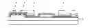
In a first step illustrated in FIG. 1, power components are fabricated on the gallium nitride substrate 1. In FIG. 1, the gallium nitride substrate 1 is formed on a first silicon substrate 2. The power component 3 shown in FIG. 1 is a transistor conventionally comprising a drain, a gate and a source formed within a layer of aluminum-gallium nitride (AlGaN). This transistor comprises three conducting lugs respectively denoted D, G and S. The electronic components fabricated can, by way of example, be “LNAs”, “DRAs” or “HPAs” respectively signifying “Low Noise Amplifier”, “Digital Research Amplifier” and “High Power Amplifier” used in systems for transmission/reception of high frequency signals.
In a second step illustrated in FIG. 2, a first passivation layer 4 is deposited, common to the whole of the GaN substrate wafer 1, covering the power components 3 and necessary for their completion and for their protection and for the fabrication of the micro-switches. The passivation layer can be made of silicon oxide (SiO2). The passivation layer thus fulfils a dual role. The power components 3 and, in particular, the regions formed of doped semiconductors are protected during the later steps of the fabrication method and especially during the steps for deposition and for elimination of the sacrificial layers of resist. The passivation layer also participates in the fabrication of the micro-switches.
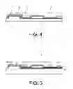
In the following step 2b shown in FIG. 3, the various electrodes 5 are formed that are needed for the operation of the micro-switches, then a second passivation layer 6 is deposited at the locations of the micro-switches. The passivation layer can be made of silicon nitride (Si3N4).
Also shown in FIG. 3, the step 2b is followed by a step 2c. The step 2c consists in locally eliminating the first passivation layer 4 on top of the electrical interconnection regions of the electronic components and in depositing a conductive metallization layer 7 on top of the said electrical interconnection regions.
In the step 3 shown in FIGS. 4 and 5, the micro-switches 10 are fabricated on said substrate. The step 3 essentially consists in depositing electrically conducting lugs 8 at the locations of the micro-switches as illustrated in FIG. 4. Then, as indicated in FIG. 5, at least one suspended membrane 9 is formed above said lugs, the whole assembly constituting the micro-switches. The membrane is formed by the deposition and the partial elimination of sacrificial layers of resist.
The micro-switch can be a switch with two channels of the type “SPDT” signifying “Single Port Dual Throw”. In FIG. 5, the two rectangles with dashed lines represent the limits of the electronic component 3 and of the micro-switch 10.
The materials used for the fabrication of the various elements can, by way of example, be gold, platinum, tungsten or titanium.
Claims
1. A method of fabrication of an electronic module comprising power electronic components fabricated on a substrate made of gallium nitride (GaN) and micro-switches using electrostatic activation of the MEMS (Micro Electro Mechanical System) type, wherein the electronic components and the micro-switches are fabricated on a single substrate of gallium nitride and the method comprises at least the following fabrication steps:
Step 1: Fabrication of the power components on the gallium nitride substrate;
Step 2: Deposition of a first common passivation layer on said components and over the entire substrate;
Step 3: Fabrication of the micro-switches on said substrate.
2. The method of fabrication of an electronic module as claimed in claim 1, wherein the step 2 is followed by a step 2b preceding the step 3, the step 2b consisting of the formation of a second passivation layer at the location of the micro-switches.
3. The method of fabrication of an electronic module as claimed in claim 2, wherein the step 2b is followed by a step 2c preceding the step 3, the step 2c consisting in locally eliminating the first passivation layer on top of the electrical interconnection regions of the electronic components and in depositing a conductive layer on top of said electrical interconnection regions.
4. The method of fabrication of an electronic module as claimed in claim 1 wherein the step 3 essentially consists in depositing electrically conducting lugs at the locations of the micro-switches and in forming on top of said lugs at least one suspended membrane, the whole assembly constituting said micro-switches.
5. The method of fabrication of an electronic module as claimed in claim 1 wherein the passivation layers are made of silicon oxide (SiO2) or of silicon nitride (Si3N4).
6. An electronic module comprising power electronic components fabricated on a substrate made of gallium nitride (GaN) using transistors of the “HEMI” (High Electron Mobility Transistor) type, wherein the power electronic components are covered by a passivation layer and that the module also comprises, on the same substrate, micro-switches using electrostatic activation of the MEMS type.
7. The electronic module as claimed in claim 6, wherein the module is a radiofrequency transmission-reception module.
8. The method of fabrication of an electronic module as claimed in claim 2, wherein the step 3 essentially consists in depositing electrically conducting lugs at the locations of the micro-switches and in forming on top of said lugs at least one suspended membrane, the whole assembly constituting said micro-switches.
9. The method of fabrication of an electronic module as claimed in claim 3, wherein the step 3 essentially consists in depositing electrically conducting lugs at the locations of the micro-switches and in forming on top of said lugs at least one suspended membrane, the whole assembly constituting said micro-switches.
10. The method of fabrication of an electronic module as claimed in claim 2, wherein the passivation layers are made of silicon oxide (SiO2) or of silicon nitride (Si3N4).
11. The method of fabrication of an electronic module as claimed in claim 3, wherein the passivation layers are made of silicon oxide (SiO2) or of silicon nitride (Si3N4).
12. The method of fabrication of an electronic module as claimed in claim 4, wherein the passivation layers are made of silicon oxide (SiO2) or of silicon nitride (Si3N4).
Images & Drawings included:
Sources:
- United States Patent and Trademark Office - verify current appl. status at the USPTO↗
Recent applications in this class:
- » 20230312337 2023-10-05
MEMS DEVICE WITH INTEGRATED CMOS CIRCUIT - » 20220289564 2022-09-15
Device for protecting FEOL element and BEOL element - » 20220185660 2022-06-16
Monolithic post complementary metal-oxide-semiconductor integration of thermoelectric-based infrared detector - » 20210206630 2021-07-08
Method for producing monolithic integration of piezoelectric micromachined ultrasonic transducers and CMOS - » 20200346925 2020-11-05
Method for integrating complementary metal-oxide-semiconductor (CMOS) devices with microelectromechanical systems (MEMS) devices using a flat surface above a sacrificial layer - » 20200216310 2020-07-09
Electrical connection to a micro electro-mechanical system - » 20200207613 2020-07-02
Complementary metal-oxide-semiconductor (CMOS) micro electro-mechanical (MEMS) microphone and method for fabricating the same - » 20200115223 2020-04-16
Device for protecting FEOL element and BEOL element - » 20200024135 2020-01-23
Method for integrating complementary metal-oxide-semiconductor (CMOS) devices with microelectromechanical systems (MEMS) devices using a flat surface above a sacrificial layer - » 20200002161 2020-01-02
Method of forming semiconductor package and semiconductor package
Recent applications for this Assignee:
- » 20190190744 2019-06-20
INFORMATION TRANSMISSION NETWORK AND CORRESPONDING NETWORK NODE - » 20170141264 2017-05-18
Method for randomly texturing a semiconductor substrate - » 20170053160 2017-02-23
Method for detecting people and/or objects in a space - » 20160371360 2016-12-22
TERMINAL FOR DISPLAYING ELEMENTS OF A DATABASE HIERARCHIZED IN N LEVELS - » 20160366563 2016-12-15
Data communication method between a plurality of aircraft - » 20160347267 2016-12-01
Transmission system for avionics application data - » 20160325856 2016-11-10
Telecommunications satellite architecture - » 20160311561 2016-10-27
Radiator deployable for a satellite stabilized on three axes - » 20160294335 2016-10-06
Radiofrequency power limiter, and associated radiofrequency emitter and/or receiver chain and low-noise amplifying stage - » 20160292939 2016-10-06
System for monitoring access to a restricted area, comprising a module housed below or above the gate