Chip assembly and chip assembling method
US20130285239A1
2013-10-31
13/559,621
2012-07-27
✅ Patent granted
US 8,860,219 B2
2014-10-14
-
-
Chandra Chaudhari
Novak Druce Connolly Bove + Quigg LLP
2032-07-27
Abstract:
A chip assembly includes a PCB and a chip positioned on the PCB. The PCB includes a number of first bonding pads. Each bonding pad includes two soldering balls formed thereon. The chip includes a number of second bonding pads, and each second bonding pad corresponds to a respective first bonding pad. The two soldering balls of each first bonding pad are electrically connected to a corresponding second bonding pad via two bonding wires, and the bonding wires are bonded to the second corresponding bonding pad by a wedge bonding manner.
Assignee:
- HON HAI PRECISION INDUSTRY CO., LTD. 12,833 🇹🇼 Tu-Cheng, Taiwan
- HON HAI PRECISION INDUSTRY CO., LTD. 10,014 🇹🇼 New Taipei, Taiwan
Applicant:
Interested in similar patents?
Get notified when new applications in this technology area are published.
Classification:
H01L2924/00012 » CPC further
Indexing scheme for arrangements or methods for connecting or disconnecting semiconductor or solid-state bodies as covered by; Technical content checked by a classifier Relevant to the scope of the group, the symbol of which is combined with the symbol of this group
H01L2224/85399 » CPC further
Indexing scheme for arrangements for connecting or disconnecting semiconductor or solid-state bodies and methods related thereto as covered by; Methods for connecting semiconductor or other solid state bodies using means for bonding being attached to, or being formed on, the surface to be connected using a wire connector; Bonding interfaces outside the semiconductor or solid-state body Material
H01L23/49816 » CPC main
Details of semiconductor or other solid state devices; Arrangements for conducting electric current to or from the solid state body in operation, e.g. leads, terminal arrangements ; Selection of materials therefor consisting of soldered constructions; Leads, on insulating substrates,; Additional leads joined to the metallisation on the insulating substrate, e.g. pins, bumps, wires, flat leads Spherical bumps on the substrate for external connection, e.g. ball grid arrays [BGA]
H01L24/48 » CPC further
Arrangements for connecting or disconnecting semiconductor or solid-state bodies; Methods or apparatus related thereto; Means for bonding being attached to, or being formed on, the surface to be connected, e.g. chip-to-package, die-attach, "first-level" interconnects; Manufacturing methods related thereto; Wire connectors; Manufacturing methods related thereto; Structure, shape, material or disposition of the wire connectors after the connecting process of an individual wire connector
H01L24/49 » CPC further
Arrangements for connecting or disconnecting semiconductor or solid-state bodies; Methods or apparatus related thereto; Means for bonding being attached to, or being formed on, the surface to be connected, e.g. chip-to-package, die-attach, "first-level" interconnects; Manufacturing methods related thereto; Wire connectors; Manufacturing methods related thereto; Structure, shape, material or disposition of the wire connectors after the connecting process of a plurality of wire connectors
H01L24/85 » CPC further
Arrangements for connecting or disconnecting semiconductor or solid-state bodies; Methods or apparatus related thereto; Methods for connecting semiconductor or other solid state bodies using means for bonding being attached to, or being formed on, the surface to be connected using a wire connector
H01L24/45 » CPC further
Arrangements for connecting or disconnecting semiconductor or solid-state bodies; Methods or apparatus related thereto; Means for bonding being attached to, or being formed on, the surface to be connected, e.g. chip-to-package, die-attach, "first-level" interconnects; Manufacturing methods related thereto; Wire connectors; Manufacturing methods related thereto; Structure, shape, material or disposition of the wire connectors prior to the connecting process of an individual wire connector
H01L25/0657 » CPC further
Assemblies consisting of a plurality of individual semiconductor or other solid state devices ; Multistep manufacturing processes thereof all the devices being of a type provided for in the same subgroup of groups - , e.g. assemblies of rectifier diodes the devices not having separate containers the devices being of a type provided for in group Stacked arrangements of devices
H01L2924/00014 » CPC further
Indexing scheme for arrangements or methods for connecting or disconnecting semiconductor or solid-state bodies as covered by; Technical content checked by a classifier the subject-matter covered by the group, the symbol of which is combined with the symbol of this group, being disclosed without further technical details
H01L2225/06506 » CPC further
Details relating to assemblies covered by the group but not provided for in its subgroups; All the devices being of a type provided for in the same subgroup of groups - the devices not having separate containers the devices being of a type provided for in group; Stacked arrangements of devices Wire or wire-like electrical connections between devices
H01L2225/0651 » CPC further
Details relating to assemblies covered by the group but not provided for in its subgroups; All the devices being of a type provided for in the same subgroup of groups - the devices not having separate containers the devices being of a type provided for in group; Stacked arrangements of devices Wire or wire-like electrical connections from device to substrate
H01L2224/05599 » CPC further
Indexing scheme for arrangements for connecting or disconnecting semiconductor or solid-state bodies and methods related thereto as covered by; Means for bonding being attached to, or being formed on, the surface to be connected, e.g. chip-to-package, die-attach, "first-level" interconnects; Manufacturing methods related thereto; Bonding areas; Manufacturing methods related thereto; Structure, shape, material or disposition of the bonding areas prior to the connecting process of an individual bonding area; External layer Material
H01L2924/30107 » CPC further
Indexing scheme for arrangements or methods for connecting or disconnecting semiconductor or solid-state bodies as covered by; Technical effects; Electrical effects Inductance
H01L2224/85203 » CPC further
Indexing scheme for arrangements for connecting or disconnecting semiconductor or solid-state bodies and methods related thereto as covered by; Methods for connecting semiconductor or other solid state bodies using means for bonding being attached to, or being formed on, the surface to be connected using a wire connector; Applying energy for connecting; Compression bonding Thermocompression bonding
H01L2924/00 » CPC further
Indexing scheme for arrangements or methods for connecting or disconnecting semiconductor or solid-state bodies as covered by
H01L23/498 IPC
Details of semiconductor or other solid state devices; Arrangements for conducting electric current to or from the solid state body in operation, e.g. leads, terminal arrangements ; Selection of materials therefor consisting of soldered constructions Leads, on insulating substrates,
H01L21/60 IPC
Processes or apparatus adapted for the manufacture or treatment of semiconductor or solid state devices or of parts thereof; Manufacture or treatment of semiconductor devices or of parts thereof the devices having at least one potential-jump barrier or surface barrier, e.g. PN junction, depletion layer or carrier concentration layer; Assembly of semiconductor devices using processes or apparatus not provided for in a single one of the subgroups - , e.g. sealing of a cap to a base of a container Attaching or detaching leads or other conductive members, to be used for carrying current to or from the device in operation
H01L23/48 IPC
Details of semiconductor or other solid state devices Arrangements for conducting electric current to or from the solid state body in operation, e.g. leads, terminal arrangements ; Selection of materials therefor
Description
BACKGROUND
1. Technical Field
The present disclosure relates to a chip assembly and a method for the chip assembly.
2. Description of Related Art
Chip assemblies include a printed circuit board (PCB) and at least one chip positioned on the PCB. To achieve predetermined functions, bonding wires are utilized to electrically connect the chip to the PCB and transmit high-frequency signals between the chip and the PCB. However, a large inductance is introduced and increases signal loss at the bonding wires when transmitting the high-frequency signals. In addition, with the development of technology, the chip becomes increasingly smaller and thus more difficult to bond bonding wires thereto.
What is needed therefore is a chip assembly and a chip assembling method addressing the limitations described.
BRIEF DESCRIPTION OF THE DRAWINGS
The components of the drawings are not necessarily drawn to scale, the emphasis instead being placed upon clearly illustrating the principles of the embodiments of the present disclosure. Moreover, in the drawings, like reference numerals designate corresponding parts throughout several views.
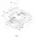
FIG. 1 is a schematic view of a chip assembly, according to an embodiment of the present disclosure.
FIG. 2 is a flowchart of a chip assembling method, according to another embodiment of the present disclosure.
DETAILED DESCRIPTION
Referring to FIG. 1, a chip assembly 100, according to an exemplary embodiment, is shown. The chip assembly 100 includes a printed circuit board (PCB) 10, a chip 20 positioned on the PCB 10, and a number of bonding wires 30.
The PCB 10 includes a supporting surface 11 for supporting the chip 20 and a number of first bonding pads 12 formed on the supporting surface 11. The first bonding pads 12 connect to circuits (not shown) formed in the PCB 10. Each first bonding pad 12 includes two soldering balls 13 formed thereon. The two soldering balls 13 are spaced from each other. In the embodiment, a distance between one of the two soldering balls 13 and the chip 20 is substantially equal to a distance between the other of the two soldering balls 13 and the chip 20.
The chip 20 is substantially rectangular-shaped. The chip 20 includes a number of second bonding pads 21, each of which corresponds to a first bonding pad 12.
In the embodiment, the number of the first bonding pads 12 is two, and the number of the second bonding pads 21 is two. In other embodiments, the number of the first bonding pads 12 and the number of the second bonding pads 12 can be changed according to different demands.
The bonding wires 30 electrically connect the chip 20 to the PCB 10. Each bonding wire 30 includes a beginning end 31 and an opposite ending end 32 between the beginning end 31 and the ending end 32. The beginning end 31 is bonded first, and the ending end 32 is bonded last. Each first bonding pad 12 is electrically connected to the corresponding second bonding pad 21 via two bonding wires 30. The two bonding wires 30 intersect to each other at the second bonding pad 21. In detail, the beginning end 31 of one bonding wire 30 is bonded on one of the soldering balls 13, and the ending end 32 of the bonding wire 30 is bonded on the corresponding second bonding pad 21; the beginning end 31 of the other bonding wire 30 is bonded on the other of the soldering balls 13, and the ending end 31 of the other bonding wire 30 is bonded on the corresponding second bonding pad 21. The ending ends 32 of the bonding wires 30 are bonding on the second bonding pad 21 by a wedge bonding manner The ending ends 32 of the two bonding wires 30 are bonded at a same position of the second bonding pad 21. The ending ends 32 form a wedge portion 33 on the second bonding pad 21.
The soldering balls 13 and the bonding wires 30 are made from a material(s) with high conductivity. In the embodiment, the soldering balls 13 and the bonding wires 30 are made from gold.
FIG. 1 only shows a chip 20 positioned on the PCB 10. However, the number of the chip on the PCB can be more than one, and the chips may have different heights. The chips also can be connected to each other by bonding wires similar as the bonding wires 30.
The chip assembly 100 electrically connects a first bonding pad 12 to a corresponding second bonding pad 21 via two shunt-wound bonding wires 30, thus an inductance between the first bonding pad 12 and the second bonding pad 21 is decreased.
Referring to FIG. 2, an embodiment of a chip assembling method is shown. The chip assembling method includes the following steps.
In step S01, a PCB is provided. The PCB includes a supporting surface and a number of first bonding pads formed on the supporting surface.
In step S02, a chip is provided. The chip includes a number of second bonding pads, and each second bonding pad corresponds to a respective first bonding pad.
In step S03, the chip is fixedly positioned on the supporting surface of the PCB.
In step S04, two soldering balls are formed on each of the first bonding pads.
In step S05, two bonding wires are provided. One end of each of the bonding wires is bonded to a respective soldering ball, and the other end of each of the bonding wires is bonded to the respective second bonding pad by a wedge bonding manner. In this embodiment, the ends of the bonding wires are bonded at the same position of the respective second bonding pad.
It should be noted that the above chip assembling method just described how to electrically connect a first bonding pad to a corresponding second bonding pad, the other first bonding pads can be electrically connected to the corresponding second bonding pads by a similar method.
It is believed that the present embodiments and their advantages will be understood from the foregoing description, and it will be apparent that various changes may be made thereto without departing from the spirit and scope of the disclosure or sacrificing all of its material advantages, the examples hereinbefore described merely being preferred or exemplary embodiments of the disclosure.
Claims
What is claimed is:1. A chip assembly, comprising:
a PCB comprising a plurality of first bonding pads, each first bonding pad comprising two soldering balls positioned thereon; and
a chip positioned on the PCB, the chip comprising a plurality of second bonding pads, each second bonding pad corresponding to a respective one of the first bonding pads;
wherein the two soldering balls of each first bonding pad are electrically connected to a corresponding second bonding pad via two bonding wires, the two bonding wires are bonded to the corresponding second bonding pad by a wedge bonding manner.
2. The chip assembly of claim 1, wherein a distance between one of the two soldering balls and the chip is substantially equal to a distance between the other of the two soldering balls and the chip.
3. The chip assembly of claim 1, wherein the bonding wires are bonded to a same position of the corresponding second bonding pad.
4. The chip assembly of claim 3, wherein ends of the bonding wires bonded to the corresponding second bonding pad form a wedge portion.
5. The chip assembly of claim 1, wherein the soldering balls and the bonding wires are made from gold.
6. A chip assembling method, comprising:
providing a PCB, the PCB comprising a plurality of first bonding pads on its supporting surface;
providing a chip, the chip comprising a plurality of second bonding pads, each second bonding pad corresponding to a respective one of the first bonding pads;
positioning the chip on the supporting surface of the PCB;
forming two soldering balls on each of the first bonding pads;
providing two bonding wires;
bonding one end of each of the two bonding wires to a respective first soldering ball; and
bonding the other end of each of the bonding wires to the corresponding second bonding pad by a wedge bonding manner
7. The chip assembling method of claim 6, wherein a distance between one of the two soldering balls and the chip is substantially equal to a distance between the other of the two soldering balls and the chip.
8. The chip assembling method of claim 6, wherein the bonding wires are bonded to a same position of the corresponding second bonding pad.
9. The chip assembling method of claim 8, wherein ends of the bonding wires bonded to the corresponding second bonding pad form a wedge portion.
10. The chip assembling method of claim 6, wherein the first soldering balls and the bonding wires are made from gold.
Images & Drawings included:


Sources:
- United States Patent and Trademark Office - verify current appl. status at the USPTO↗
Similar patent applications:
- » 20240078406
CHIP ASSEMBLY, METHOD FOR FORMING A CHIP ASSEMBLY, AND METHOD FOR USING A CHIP ARRANGEMENT - » 20150061100
Semiconductor arrangement, method for producing a number of chip assemblies, method for producing a semiconductor arrangement and method for operating a semiconductor arrangement - » 20130242518
Chip assembly and chip assembling method - » 20120217287
Flip chip assembly method employing post-contact differential heating - » 10164116
Semiconductor chip assemblies, methods of making same and components for same - » 20130285243
Easily assembled chip assembly and chip assembling method - » 20140283909
CONCENTRATING PHOTOVOLTAIC CHIP ASSEMBLY, METHOD FOR MANUFACTURING THE SAME, AND CONCENTRATING PHOTOVOLTAIC ASSEMBLY WITH SAME - » 9656690
Semiconductor chip assemblies, methods of making same and components for same - » 20080274589
Wafer-level flip-chip assembly methods - » 20230400788
CHIP ASSEMBLY AND METHOD OF MAKING A CHIP ASSEMBLY
Recent applications in this class:
- » 20130328179 2013-12-12
Integrated circuit packaging system with warpage preventing mechanism and method of manufacture thereof - » 20130292832 2013-11-07
SEMICONDUCTOR PACKAGE AND FABRICATION METHOD THEREOF - » 20130277855 2013-10-24
HIGH DENSITY 3D PACKAGE - » 20130277839 2013-10-24
CHIP PACKAGE AND METHOD FOR ASSEMBLING SAME - » 20130256884 2013-10-03
GRID FAN-OUT WAFER LEVEL PACKAGE AND METHODS OF MANUFACTURING A GRID FAN-OUT WAFER LEVEL PACKAGE - » 20130249118 2013-09-26
Integrated circuit packaging system with a grid array with a leadframe and method of manufacture thereof - » 20130241071 2013-09-19
Semiconductor device and method of forming compliant conductive interconnect structure in flipchip package - » 20130234318 2013-09-12
Semiconductor device and method of forming non-linear interconnect layer with extended length for joint reliability - » 20130211776 2013-08-15
Ball grid structure - » 20130181342 2013-07-18
SEMICONDUCTOR PACKAGE
Recent applications for this Assignee:
- » 20250218287 2025-07-03
METHOD OF GENERATING AND PROMPTING TRAFFIC INFORMATION, AND ROADSIDE DEVICE THEREOF - » 20250178535 2025-06-05
METHOD FOR CONSTRUCTING 3D PANORAMIC VIEW MODEL, VEHICLE-MOUNTED DEVICE, AND STORAGE MEDIUM - » 20250074444 2025-03-06
METHOD FOR EARLY WARNING A BLIND AREA, ELECTRONIC DEVICE AND STORAGE MEDIUM - » 20240416754 2024-12-19
DISPLAY CONTROL DEVICE, DISPLAY EQUIPMENT, AND VEHICLE EMPLOYING DEVICE - » 20240411051 2024-12-12
Light-emitting device array and optical transceiver system having the same - » 20240324114 2024-09-26
DISPLAY CONTROL DEVICE AND VEHICLE EMPLOYING DEVICE - » 20240295957 2024-09-05
METHOD FOR CONTROLLING ELECTRONIC DEVICE, ELECTRONIC DEVICE AND COMPUTER STROAGE MEDIUM EMPLOYING METHOD - » 20240257357 2024-08-01
METHOD FOR DETECTING OBSTACLES, ELECTRONIC DEVICE, AND STORAGE MEDIUM - » 20240203133 2024-06-20
LANE LINE RECOGNITION METHOD, ELECTRONIC DEVICE AND STORAGE MEDIUM - » 20240194999 2024-06-13
Robot using limiting device for locking battery