PACKAGE SUBSTRATE AND CHIP PACKAGE USING THE SAME
US20140118978A1
2014-05-01
13/659,916
2012-10-25
Abstract:
A package substrate is disclosed. The package substrate includes a base layer and a dam structure or a dent structure on at least one side of the base layer. The base layer may be a CCL core, a molding compound, or an epoxy base.
Interested in similar patents?
Get notified when new applications in this technology area are published.
Classification:
H01L23/13 » CPC further
Details of semiconductor or other solid state devices; Mountings, e.g. non-detachable insulating substrates characterised by the shape
H01L23/3157 » CPC further
Details of semiconductor or other solid state devices; Encapsulations, e.g. encapsulating layers, coatings, e.g. for protection characterised by the arrangement or shape Partial encapsulation or coating
H01L23/49816 » CPC further
Details of semiconductor or other solid state devices; Arrangements for conducting electric current to or from the solid state body in operation, e.g. leads, terminal arrangements ; Selection of materials therefor consisting of soldered constructions; Leads, on insulating substrates,; Additional leads joined to the metallisation on the insulating substrate, e.g. pins, bumps, wires, flat leads Spherical bumps on the substrate for external connection, e.g. ball grid arrays [BGA]
H01L24/48 » CPC further
Arrangements for connecting or disconnecting semiconductor or solid-state bodies; Methods or apparatus related thereto; Means for bonding being attached to, or being formed on, the surface to be connected, e.g. chip-to-package, die-attach, "first-level" interconnects; Manufacturing methods related thereto; Wire connectors; Manufacturing methods related thereto; Structure, shape, material or disposition of the wire connectors after the connecting process of an individual wire connector
H01L2224/73207 » CPC further
Indexing scheme for arrangements for connecting or disconnecting semiconductor or solid-state bodies and methods related thereto as covered by; Means for bonding being of different types provided for in two or more of groups; Location after the connecting process on the same surface Bump and wire connectors
H01L2224/8592 » CPC further
Indexing scheme for arrangements for connecting or disconnecting semiconductor or solid-state bodies and methods related thereto as covered by; Methods for connecting semiconductor or other solid state bodies using means for bonding being attached to, or being formed on, the surface to be connected using a wire connector; Post-treatment of the connector or wire bonding area Applying permanent coating, e.g. protective coating
H01L2224/85951 » CPC further
Indexing scheme for arrangements for connecting or disconnecting semiconductor or solid-state bodies and methods related thereto as covered by; Methods for connecting semiconductor or other solid state bodies using means for bonding being attached to, or being formed on, the surface to be connected using a wire connector; Post-treatment of the connector or wire bonding area Forming additional members, e.g. for reinforcing
Y10T428/24612 » CPC further
Stock material or miscellaneous articles; Structurally defined web or sheet [e.g., overall dimension, etc.] including variation in thickness Composite web or sheet
H01L2924/15311 » CPC further
Indexing scheme for arrangements or methods for connecting or disconnecting semiconductor or solid-state bodies as covered by; Details of package parts other than the semiconductor or other solid state devices to be connected; Die mounting substrate; Connection portion the connection portion being formed only on the surface of the substrate opposite to the die mounting surface being a ball array, e.g. BGA
H01L2224/73215 » CPC further
Indexing scheme for arrangements for connecting or disconnecting semiconductor or solid-state bodies and methods related thereto as covered by; Means for bonding being of different types provided for in two or more of groups; Location after the connecting process on the same surface Layer and wire connectors
H01L2924/181 » CPC further
Indexing scheme for arrangements or methods for connecting or disconnecting semiconductor or solid-state bodies as covered by; Details of package parts other than the semiconductor or other solid state devices to be connected Encapsulation
H01L2924/00 » CPC further
Indexing scheme for arrangements or methods for connecting or disconnecting semiconductor or solid-state bodies as covered by
H01L2224/45099 » CPC further
Indexing scheme for arrangements for connecting or disconnecting semiconductor or solid-state bodies and methods related thereto as covered by; Means for bonding being attached to, or being formed on, the surface to be connected, e.g. chip-to-package, die-attach, "first-level" interconnects; Manufacturing methods related thereto; Wire connectors; Manufacturing methods related thereto; Structure, shape, material or disposition of the wire connectors prior to the connecting process of an individual wire connector; Core members of the connector Material
H01L2924/00014 » CPC further
Indexing scheme for arrangements or methods for connecting or disconnecting semiconductor or solid-state bodies as covered by; Technical content checked by a classifier the subject-matter covered by the group, the symbol of which is combined with the symbol of this group, being disclosed without further technical details
H01L2224/05599 » CPC further
Indexing scheme for arrangements for connecting or disconnecting semiconductor or solid-state bodies and methods related thereto as covered by; Means for bonding being attached to, or being formed on, the surface to be connected, e.g. chip-to-package, die-attach, "first-level" interconnects; Manufacturing methods related thereto; Bonding areas; Manufacturing methods related thereto; Structure, shape, material or disposition of the bonding areas prior to the connecting process of an individual bonding area; External layer Material
H05K1/02 » CPC main
Printed circuits Details
H05K1/02 » CPC main
Printed circuits Details
B32B3/30 IPC
Layered products comprising a layer with external or internal discontinuities or unevennesses, or a layer of non-planar form ; Layered products having particular features of form characterised by a particular shape of the outline of the cross-section of a continuous layer; characterised by a layer with cavities or internal voids ; characterised by an apertured layer characterised by a layer formed with recesses or projections, e.g. hollows, grooves, protuberances, ribs
H05K1/18 IPC
Printed circuits Printed circuits structurally associated with non-printed electric components
H05K1/18 IPC
Printed circuits Printed circuits structurally associated with non-printed electric components
Description
BACKGROUND OF THE INVENTION
1. Field of the Invention
The present invention relates to semiconductor devices. More particularly, the present invention relates to a package substrate and a chip package structure.
2. Description of the Prior Art
In the integrated circuit (IC) packaging industry, there is a continuous desire to provide higher and higher density IC packages for semiconductor die having increasing numbers of input/output (I/O) terminal pads. When using a conventional wire bonding packaging technique, the pitch, or spacing between adjacent bonding wires becomes finer and finer as the number of I/O terminal pads increases for a given size die.
As known in the art, semiconductor die is typically sealed within a package of moldable material to protect it from environmental stresses. The moldable material is fed into cavities of a mold, thus flowing over the semiconductor die. The moldable material is then hardened to encapsulate the semiconductor die. However, the moldable material may bleed onto the solder mask. The mold bleed can adversely affect bonding of the external contacts to the bonding sites. The mold bleed can also adversely affect the electrical connections to the external contacts, and the cosmetic appearance of the package. Additionally, a subsequent process may be necessary to remove the mold bleed from the substrate surface and the equipment.
SUMMARY OF THE INVENTION
In one aspect, the present invention provides a package substrate including a base layer and a dam structure or a dent structure on at least one side of the base layer. The base layer may be a CCL core, a molding compound, or an epoxy base.
In another aspect, the present invention provides a package substrate including a base layer having a first side and a second side that is opposite to the first side; a first solder mask on a first side of the base layer; and a second solder mask on a second side of the base layer, wherein at least one of the first and second solder masks has thereon a dam structure and a dent structure.
In accordance with another aspect of the invention, a chip package includes a package substrate having a chip mounting side and a bottom side that is opposite to the chip mounting side; a semiconductor chip mounted on the chip mounting side; and a dam structure and a dent structure on the bottom side of the package substrate.
These and other objectives of the present invention will no doubt become obvious to those of ordinary skill in the art after reading the following detailed description of the preferred embodiment that is illustrated in the various figures and drawings.
BRIEF DESCRIPTION OF THE DRAWINGS
FIG. 1 is schematic, cross-sectional diagram showing a germane portion of a package substrate in accordance with one embodiment of this invention.
FIG. 2 is a schematic, cross-sectional view of a window BGA package for DRAM chips in accordance with another embodiment of this invention.
DETAILED DESCRIPTION
FIG. 1 is schematic, cross-sectional diagram showing a germane portion of a package substrate in accordance with one embodiment of this invention. As shown in FIG. 1, the package substrate 1 has a base layer 10 that may comprise a copper clay laminate (CCL) core and at least one layer of circuit pattern on the CCL core. The CCL core and the circuit pattern are not shown explicitly for the sake of simplicity. It is well known that circuit patterns on different sides of the core may be interconnected by plated through holes (PTHs), and that the package substrate 1 may comprise multiple layers of circuit patterns. It is to be understood that the package substrate 1 may be any other type of substrate, for example, a substrate merely composed of molding compound without using a CCL core or a solder mask. Alternatively, the base layer 10 may be an epoxy base.
According to the embodiment, a first solder mask 12 is provided on a first side of the base layer 10. A dam structure 12a may be formed on the first solder mask 12. The dam structure 12a protrudes from a major surface of the first solder mask 12 and may have a width w1 ranging, for example, between 0.001 mm and 2 mm, and a height h1 ranging, for example, between 0.001 mm and 2 mm. When viewed from the above, the dam structure 12a may have various shapes, for example, line shape, serpentine shape, or curved shape. It is to be understood that the dam structure 12a may be formed on a core material layer, a molding compound or a metal layer, depending upon the type of substrate chosen for the semiconductor package. Further, it is to be understood that in some cases the dam structure 12a may be made of a material that is different from that of the underlying layer (label 12). For example, the underlying layer 12 may be made of epoxy, CCL, BT resin, metal or solder mask, and is not limited to solder mask.
Optionally, a dent structure 12b may be provided adjacent to the dam structure 12a. The dent structure 12b may have a width w2 ranging, for example, between 0.001 mm and 2 mm, and a height h2 ranging, for example, between 0.001 mm and 2 mm. The dent structure 12b may have a shape selected from the group consisting of line shape, serpentine shape and curved shape. According to the embodiment, the dam structure 12a may be substantially in parallel with the dent structure 12b. The second side of the base layer 10 may be covered with a second solder mask 14. It is to be understood that although not shown in this figure, the aforesaid dam structure and/or dent structure may also be applied onto the second solder mask 14.
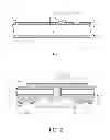
FIG. 2 is a schematic, cross-sectional view of an exemplary window BGA package for DRAM chips in accordance with another embodiment of this invention. As shown in FIG. 2, the chip package 100 comprises the package substrate 1 having the features substantially as described in FIG. 1. More specifically, the package substrate 1 has a chip mounting side 100a and a bottom side 100b that is opposite to the chip mounting side 100a. A semiconductor chip 20 such as a DRAM chip or die is mounted on the chip mounting side 100a by applying an adhesive layer 24 on the top surface of the second solder mask 14 to attach the semiconductor chip 20 on the chip mounting side 100a. In another embodiment, the label 24 may represent a bump, and no adhesive is used. In still another embodiment, the label 24 may represent both bump and adhesive. Likewise, the layer 14 may be made of epoxy, CCL, BT resin, metal or solder mask, and is not limited to solder mask.
An opening 10a, which is also referred to as “window”, is formed in the package substrate 1 between the chip mounting side 100a and the bottom side 100b. The active surface of the semiconductor chip 20 is electrically coupled to the bottom side 100b of the package substrate 1 using bond wires 26 that pass through the opening 10a. The bond wires 26 electrically connect the bond pads 22 on the active surface of the semiconductor chip 20 to the traces or bond fingers (not shown) on the bottom side 100b of the package substrate 1. The first solder mask 12 may provide electrical isolation and physical protection for the traces. It is to be understood that the layer 12 may be made of epoxy, CCL, BT resin, metal or solder mask, and is not limited to solder mask. A molding compound 30 is used to fill the opening 10a and encapsulate the bond pads 22, the bond wires 26, and the bond fingers on the bottom side 100b of the package substrate 1.
According to the embodiment, a dam structure 12a may be formed on the first solder mask 12. The dam structure 12a protrudes from a major surface of the first solder mask 12. When viewed from the above, the dam structure 12a may have various shapes, for example, line shape, serpentine shape, or curved shape. Optionally, a dent structure 12b may be provided adjacent to the dam structure 12a, and in this case, the dent structure 12b may be closer to the opening 10a than the dam structure 12a. The dent structure 12b in the first solder mask 12 can guide the mold bleed to a buffer area (not shown) during molding process. The dam structure 12a effectively stops and blocks the mold bleed from contaminating the solder ball implanting area 210, in which a plurality of solder balls 200 are disposed, on the other side of the dam structure 12a. The proposed structure also can prevent bleeding of paste-like materials. Further, although not shown in this figure, it is to be understood that the dam structure and/or the dent structure may be provided on the chip mounting side.
Those skilled in the art will readily observe that numerous modifications and alterations of the device and method may be made while retaining the teachings of the invention. Accordingly, the above disclosure should be construed as limited only by the metes and bounds of the appended claims.
Claims
What is claimed is:1. A package substrate, comprising:
a base layer; and
a dam structure and/or a dent structure on at least one side of the base layer.
2. The package substrate according to claim 1 wherein the base layer comprises a CCL core, a molding compound, or an epoxy base.
3. The package substrate according to claim 1 wherein the dam structure has a shape selected from the group consisting of line shape, serpentine shape and curved shape.
4. The package substrate according to claim 1 wherein the dent structure has a shape selected from the group consisting of line shape, serpentine shape and curved shape.
5. A package substrate, comprising:
a base layer having a first side and a second side that is opposite to the first side;
a first solder mask on a first side of the base layer; and
a second solder mask on a second side of the base layer, wherein at least one of the first and second solder masks has thereon a dam structure and/or a dent structure.
6. The package substrate according to claim 5 wherein the base layer comprises a CCL core and at least one layer of circuit pattern.
7. The package substrate according to claim 5 wherein the dam structure has a shape selected from the group consisting of line shape, serpentine shape and curved shape.
8. The package substrate according to claim 5 wherein the dam structure is arranged substantially in parallel with the dent structure.
9. A chip package, comprising:
a package substrate having a chip mounting side and a bottom side that is opposite to the chip mounting side;
a semiconductor chip mounted on the chip mounting side; and
a dam structure and/or a dent structure on either chip mounting side or the bottom side of the package substrate.
10. The chip package according to claim 9 wherein the dam structure and/or the dent structure are formed on a solder mask, a molding compound, or a metal.
11. The chip package according to claim 10 wherein the dam structure has a shape selected from the group consisting of line shape, serpentine shape and curved shape.
12. The chip package according to claim 10 wherein the dent structure has a shape selected from the group consisting of line shape, serpentine shape and curved shape.
Images & Drawings included:

Sources:
- United States Patent and Trademark Office - verify current appl. status at the USPTO↗
Similar patent applications:
- » 20160379957
Substrate for mounting a chip and chip package using the substrate - » 20160380168
Chip substrate comprising a groove portion and chip package using the chip substrate - » 20140175665
Chip package using interposer substrate with through-silicon vias - » 20150041182
PACKAGE SUBSTRATE AND CHIP PACKAGE USING THE SAME - » 20060079019
Method for manufacturing wafer level chip scale package using redistribution substrate - » 20130032939
Chip package structure using flexible substrate - » 20130309812
Integrated chip package structure using ceramic substrate and method of manufacturing the same - » 20080265401
Integrated chip package structure using organic substrate and method of manufacturing the same - » 20050046033
Tape circuit substrate and semiconductor chip package using the same - » 20090261368
LED chip package structure using a substrate as a lampshade and method for making the same
Recent applications in this class:
- » 20250133648 2025-04-24
COMPUTER HARDWARE INSTALLATION AND REMOVAL TOOL - » 20240422891 2024-12-19
PRINTED CIRCUIT BOARD ASSEMBLY AND METHOD FOR MANUFACTURING PRINTED CIRCUIT BOARD ASSEMBLY - » 20230284370 2023-09-07
PROTECTION UNIT AND DISPLAY DEVICE INCLUDING THE SAME - » 20230239992 2023-07-27
REINFORCING BOARD AND DISPLAY APPARATUS HAVING THE SAME - » 20220295626 2022-09-15
WIRELESS POWER SUPPLY WIRING CIRCUIT BOARD AND BATTERY MODULE - » 20210289613 2021-09-16
Structural element fixing structure and fixing element thereof - » 20200053864 2020-02-13
METHOD OF MANUFACTURING A PRINTED CIRCUIT BOARD - » 20200045805 2020-02-06
Plastic injection molded potting cups and related methods - » 20190037680 2019-01-31
Chip mounter, electronic circuit substrate, and power module - » 20180279462 2018-09-27
Printed circuit board component cover