MR device with synthetic free layer structure
US20140138783A1
2014-05-22
14/166,373
2014-01-28
✅ Patent granted
US 9,013,016 B2
2015-04-21
-
-
Samuel Gebremariam
Saile Ackerman LLC | Stephen B. Ackerman
2034-01-28
Abstract:
A magneto-resistive device having a large output signal as well as a high signal-to-noise ratio is described along with a process for forming it. This improved performance was accomplished by expanding the free layer into a multilayer laminate comprising at least three ferromagnetic layers separated from one another by antiparallel coupling layers. The ferromagnetic layer closest to the transition layer must include CoFeB while the furthermost layer is required to have low Hc as well as a low and negative lambda value. One possibility for the central ferromagnetic layer is NiFe but this is not mandatory.
Inventors:
- Tong Zhao 49 🇺🇸 Fremont, CA, United States
- Min Li 112 🇺🇸 Dublin, CA, United States
- Kunliang Zhang 94 🇺🇸 Fremont, CA, United States
- Hui-Chaun Wang 1 🇺🇸 Pleasanton, CA, United States
- Yu-Chen Zhou 5 🇺🇸 San Jose, CA, United States
Assignee:
- Headway Technologies, Inc. 1,073 🇺🇸 Milpitas, CA, United States
Applicant:
Interested in similar patents?
Get notified when new applications in this technology area are published.
Classification:
H01L43/08 » CPC main
Devices using galvano-magnetic or similar magnetic effects; Processes or apparatus specially adapted for the manufacture or treatment thereof or of parts thereof Magnetic-field-controlled resistors
G01R33/098 » CPC further
Arrangements or instruments for measuring magnetic variables; Measuring direction or magnitude of magnetic fields or magnetic flux using galvano-magnetic devices; Magnetoresistive devices comprising tunnel junctions, e.g. tunnel magnetoresistance sensors
G01R33/09 IPC
Arrangements or instruments for measuring magnetic variables; Measuring direction or magnitude of magnetic fields or magnetic flux using galvano-magnetic devices Magnetoresistive devices
G11B5/39 IPC
Recording by magnetisation or demagnetisation of a record carrier; Reproducing by magnetic means; Record carriers therefor; Structure or manufacture of heads, e.g. inductive; Structure or manufacture of flux-sensitive heads, i.e. for reproduction only; Combination of such heads with means for recording or erasing only using magneto-resistive devices or effects
H01F10/32 IPC
Thin magnetic films, e.g. of one-domain structure Spin-exchange-coupled multilayers, e.g. nanostructured superlattices
H01F41/30 IPC
Apparatus or processes specially adapted for manufacturing or assembling magnets, inductances or transformers; Apparatus or processes specially adapted for manufacturing materials characterised by their magnetic properties for applying magnetic films to substrates for applying nanostructures, e.g. by molecular beam epitaxy [MBE]
B82Y25/00 » CPC further
Nanomagnetism, e.g. magnetoimpedance, anisotropic magnetoresistance, giant magnetoresistance or tunneling magnetoresistance
B82Y40/00 » CPC further
Manufacture or treatment of nanostructures
G11B5/3906 » CPC further
Recording by magnetisation or demagnetisation of a record carrier; Reproducing by magnetic means; Record carriers therefor; Structure or manufacture of heads, e.g. inductive; Structure or manufacture of flux-sensitive heads, i.e. for reproduction only; Combination of such heads with means for recording or erasing only using magneto-resistive devices or effects using magnetic thin film layers or their effects, the films being part of integrated structures Details related to the use of magnetic thin film layers or to their effects
G11C11/16 » CPC further
Digital stores characterised by the use of particular electric or magnetic storage elements; Storage elements therefor using magnetic elements using elements in which the storage effect is based on magnetic spin effect
H01F10/3254 » CPC further
Thin magnetic films, e.g. of one-domain structure; Spin-exchange-coupled multilayers, e.g. nanostructured superlattices; Exchange coupling of magnetic film pairs via a very thin non-magnetic spacer, e.g. by exchange with conduction electrons of the spacer the spacer being semiconducting or insulating, e.g. for spin tunnel junction [STJ]
H01F10/3272 » CPC further
Thin magnetic films, e.g. of one-domain structure; Spin-exchange-coupled multilayers, e.g. nanostructured superlattices; Exchange coupling of magnetic film pairs via a very thin non-magnetic spacer, e.g. by exchange with conduction electrons of the spacer the exchange coupling being asymmetric, e.g. by use of additional pinning, by using antiferromagnetic or ferromagnetic coupling interface, i.e. so-called spin-valve [SV] structure, e.g. NiFe/Cu/NiFe/FeMn by use of anti-parallel coupled [APC] ferromagnetic layers, e.g. artificial ferrimagnets [AFI], artificial [AAF] or synthetic [SAF] anti-ferromagnets
H01F41/302 » CPC further
Apparatus or processes specially adapted for manufacturing or assembling magnets, inductances or transformers; Apparatus or processes specially adapted for manufacturing materials characterised by their magnetic properties for applying magnetic films to substrates for applying nanostructures, e.g. by molecular beam epitaxy [MBE] for applying spin-exchange-coupled multilayers, e.g. nanostructured superlattices
H01L43/12 » CPC further
Devices using galvano-magnetic or similar magnetic effects; Processes or apparatus specially adapted for the manufacture or treatment thereof or of parts thereof Processes or apparatus specially adapted for the manufacture or treatment of these devices or of parts thereof
H01L29/82 IPC
Semiconductor devices adapted for rectifying, amplifying, oscillating or switching, or capacitors or resistors with at least one potential-jump barrier or surface barrier, e.g. PN junction depletion layer or carrier concentration layer; Details of semiconductor bodies or of electrodes thereof; Multistep manufacturing processes therefor; Types of semiconductor device ; Multistep manufacturing processes therefor controllable by variation of the magnetic field applied to the device
Description
This is a Divisional application of US patent application serial number U.S. Ser. No. 12/313,351, filed on Nov. 19, 2008, which is herein incorporated by reference in its entirety, and assigned to a common assignee.
FIELD OF THE INVENTION
The invention relates to the general field of magneto resistance (MR) with particular reference to the micro-structure of the free layer.
BACKGROUND OF THE INVENTION
Magnetic tunneling junction (MTJ) is a key component of both magnetic recording heads and magnetic random access memory (MRAM). A typical MTJ structure for a recording head or for an MRAM application is schematically illustrated in FIG. 1, as follows:
Buffer layer 11, antiferromagnetic layer (AFM) 12, an outer pinned layer, Ru, (neither shown) inner pinned layer 13 (the reference layer), tunnel barrier layer 14, free layer 15, and capping layer 16. In this structure, free layer 15 serves as the sensing layer which responds to external fields (specifically those stored in the media) while inner pinned layer 13 remains fixed and serves as reference layer. The electrical resistance through barrier (i.e. insulating) layer 14 varies with the relative orientation of the free layer moment relative to the reference layer moment thereby converting magnetic information stored in the media into electrical signals.
For effective operation as part of a magnetic recoding head, the basic requirements for TMR sensors are as following:
1) Low resistance·area product (RA)
2) High magneto resistance (MR) ratio
3) A soft free layer having low magnetostriction
4) Low interlayer coupling through the barrier layer.
5) Strongly pinned reference layer.
MgO-based MTJs are promising candidates for achieving high recording density and/or high frequency application because their TMR ratio is significantly higher than those of AlOx or TiOx based MTJs. S. Yuasa et al [1] and S. S. Parkin et al. [2] demonstrated that MR ratios around 200% can be achieved at room temperature in epitaxial Fe(001)/MgO(001)/Fe(001) and with polycrystalline FeCo/MgO/(Fe70Co30)80B20 MTJs.
Yuasa et al. [3] have also reported that TMR ratios as high as 410% at room temperature can be achieved in fully epitaxial Fe(001)/Co(001)/MgO(001)/Co structures. Meanwhile, D. D. Djayaprawira et al [4] showed that MTJs of CoFeB/MgO(001)/CoFeB structure made by conventional sputtering can also have a very high MR ratio (230%) with the added advantage of greater feasibility and uniformity. For low RA applications, the MR ratio of CoFeB/Mg/MgO/CoFeB MTJs can reach 138% at RA=2.4 ohm·μm2 was achieved by K. Tsunekawa et al [5] by inserting a DC-sputtered metallic Mg layer in between the bottom CoFeB and the rf-sputtered MgO, an idea initially proposed by T. Linn et al. [6] to prevent oxidation of the bottom electrode (CoFe) in a CoFe/MgO/reactive sputtering/NiFe structure. Also, Ta getter-presputtering prior to the rf-sputtered MgO layer can achieve 55% TMR with an RA of 0.4 ohm·micron2 as recently reported by Y. Nagamine et al. [7]. An alternative way to form a low RA MgO barrier is to deposit two metallic Mg layers with a natural oxidation process in between as we previously proposed for the benefit of better process control and MRR uniformity.
CoFeB material has been used in MgO based MTJs to achieve a magnetically soft free layer having a high MR ratio. High MR ratio and low RA has been demonstrated in MgO MTJs with CoFeB free layer. It was also demonstrated that insertion of a thin CoFe layer between MgO barrier and CoFeB facilitates getting a high MR ratio even at low annealing temperatures (ca. 300° C.). However, there remains a concern that a CoFeB free layer will have a high positive magnetostriction coefficient (lambda).
There are several possible ways to reduce lambda in a CoFeB based free layer. As shown elsewhere, lambda can be reduced by replacing CoFeB with CoB or by adjusting the CoFeB composition. However, magnetic softness deteriorated at the high annealing temperature needed to achieve a high MR ratio. To tackle this issue, a special annealing procedure was developed whereby a relatively high dR/R could be achieved while the free layer was still soft. An alternative approach for reducing lambda is to add a NiFe layer, which has negative lambda and is magnetically soft, on top of the CoFeB in the free layer. However, CoFeB/NiFe-type free layer structure is not usable because direct contact between CoFeB and NiFe causes a drastic drop in MR ratio.
H. Wang et al have proposed to use CoFe/CoFeB/Ta/NiFe as a free layer with high dR/R. In this structure, high dR/R can be achieved because the CoFeB is separated from the NiFe by a Ta insertion layer. The CoFe\CoFeB and NiFe layers are magnetically coupled through orange-peel type coupling, which tend to align magnetic moments to be parallel. However, this coupling is relatively weak and, in the case of real devices, has to compete with magnetostatic coupling from the edge of two layers which tend to align these two layers anti-parallel. As a result, magnetic noise for this kind of structure is relatively high. So although signal amplitude is high, improvement in signal-to-noise ratio is limited.
REFERENCES
- 1. S. Yuasa et al “Giant room-temperature magnetoresistance in single-crystal Fe/MgO/Fe magnetic tunnel junctions”, Nature Materials 3, 868-871 (2004).
- 2. S. S. P. Parkin et al, “Giant tunnelling magnetoresistance at room temperature with MgO (100) tunnel barriers”, Nature Materials 3, 862-867 (2004).
- 3. S. Yuasa et al. “Giant tunneling magnetoresistance up to 410% at room temperature in fully epitaxial Co/MgO/Co magnetic tunnel junctions with bcc Co(001) electrodes”, Applied Physics Letters 89, 042505 (2006).
- 4. D. D. Djayaprawira et al. “230% room-temperature magnetoresistance in CoFeB/MgO/CoFeB magnetic junctions”, Applied Physics Letters 86, 092502 (2005).
- 5. K. Tsunekawa et al. “Giant tunneling magnetoresistance effect in low-resistance CoFeB/MgO(001)/CoFeB magnetic tunnel junctions for read-head applications” Applied Physics Letters 87, 072503 (2005).
- 6. T. Linn et al., “Method of forming a barrier layer of a tunneling magnetoresistvie sensor”, U.S. Pat. No. 0,101,978 A1 (May 27, 2004).
- 7. Y. Nagamine et al. “Ultralow resistance-area product of 0.4 ohm**μm̂2 and high magnetoresistance above 50% in CoFeB/MgO/CoFeB magnetic junctions” Applied Physics Letter 89 162507 (2006).
- 8. T. Zhao et al. Headway Invention Proposal HT05-045—“Low Resistance Tunneling
Magnetoresistive Sensor With Natural-Oxidized Double MgO Barrier”
- 9. H. Wang et al Headway Invention Proposal HT07-040 “TMR Sensor with Low magnetostriction Free layer
- 10. H. Wang et al Headway Invention Proposal HT07-028 “Novel Free Layer Design for TMR/CPP Device”.
A routine search of the prior art was performed with the following references of interest being found:
In U.S. Patent Application 2008/0117553, Carey et al. disclose a free layer comprising CoFe/spacer/NiFe/spacer/CoFe where the spacer is Cu, Au, or Ag and where a third element can be alloyed with the CoFe or NiFe. Additional discussion of this reference appears later in connection with TABLE I.
In U.S. Pat. No. 7,130,166, Gill shows a three-layer free layer where the first and third layers are CoFe/NiFe and the second layer is NiFe, but any of these layers can be NiFe, CoFe, or an CoFe/NiFe stack. The layers are separated by Ru. U.S. Pat. No. 7,141,314 (Zhang et al—Headway) teaches free layer laminates of CoFe and FeCo with spacer layers of Cu. In U.S. Pat. No. 7,149,105, Brown et al. disclose a free layer comprising NiFe and CoFeB separated by a nonmagnetic spacer such as Ru, having a thickness of 2-30 Angstroms.
U.S. Patent Application 2007/0097561 (Miyauchi et al.) shows a free layer comprising alloys of Co, Fe, Ni having a nonmagnetic layer in between while in U.S. Patent Application 2006/0291108, Sbiaa et al. describe a free layer containing a nonmagnetic spacer such as Ru, Rh, Ag, Cu.
SUMMARY OF THE INVENTION
It has been an object of at least one embodiment of the present invention to provide a magneto-resistive device having a large output signal as well as a high signal-to-noise ratio.
Another object of at least one embodiment of the present invention has been that said device be any of CIP-GMR, CPP-GMR, MTJ, and TMR devices.
Still another object of at least one embodiment of the present invention has been to provide a process for forming said magneto-resistive device.
A further object of at least one embodiment of the present invention has been for said process be fully compatible with existing processes for forming magneto-resistive devices.
These objects have been achieved by expanding the free layer into a multilayer laminate comprising at least three ferromagnetic layers separated from one another by antiparallel coupling layers, whereby the central ferromagnetic layer has a magnetization direction that is antiparallel to that of the two outer layers.
Additionally, the first of these three ferromagnetic layers, the one closest to the transition layer, must include (or consist entirely of) CoFeB while the third layer is required to have low Hc as well as a low and negative lambda value. One possibility for the central ferromagnetic layer is NiFe but this is not mandatory.
Processes for forming both the expanded free layer as well as the full device are also described.
BRIEF DESCRIPTION OF THE DRAWINGS
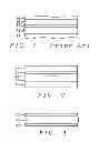
FIG. 1 is a schematic cross-section of a TMR stack of the prior art, including simple free layer 15.
FIG. 2 shows how free layer 15 of the prior art has been expanded into a laminate of three antiparallel coupled ferromagnetic layers.
FIG. 3 shows how the first of the ferromagnetic layers of FIG. 2 has been further expanded into a three layer laminate.
DESCRIPTION OF THE PREFERRED EMBODIMENTS
The present invention discloses a free layer structure comprising at least three magnetic layers whose magnetic moments are antiparallel coupled through Ru layers. This is illustrated in FIG. 2 which shows how the simple free layer 15 seen in FIG. 1 has been expanded to become a more complex structure. Seen in FIG. 2 are ferromagnetic layers mag1, mag2, and mag3 which have been designated as layers 21, 23, and 25 respectively. The magnetizations of layers 21 and 23 are antiparallel to each other as are those of layers 25 and 23, the required antiparallel coupling between the two pairs of layers being provided by Ru layers 22 and 24, respectively. Note that, while Ru is generally preferred, acceptable antiparallel coupling can also be achieved by using other materials such as Rh, Cu, Cr, or Ir in place of Ru. As with Ru, their thickness should be in a range of from 4-10 Å.
Mag1 can be made of single layer or combination of: CoxFe1−x(x=0˜100%), (CoxFe1−x)1−yBy (x=0˜100%, y=10˜40%) or their alloys with third or forth elements, such as Ni, Ta, Mn, Ti, W, Zr, Hf, Tb. For example, CoFeB, CoFe\CoFeB or CoFe\CoFeB\CoFe. The thickness for each layer may be 1˜40 Å. Materials or structures that give higher dR/R are preferred.
Mag2 can be a single layer or a combination of: NixFe1−x (x=0˜100) CoxFe1−x(x=0˜100%) and their alloys with third or fourth elements, such as Ni, Ta, Mn, Ti, W, Zr, Hf, Tb or B. For example, CoFe, NiFe or CoFe\NiFe\CoFe. The thickness for each layer may be 1˜30 A. Materials or structures with low or negative lambda that promote strong coupling through spacers are preferred.
Mag3 can be a single layer or combination of: NixFe1−x (x=0˜100) CoxFe1−x(x=0˜100%), their alloys with third or fourth elements, such as Ni, Ta, Mn, Ti, W, Zr, Hf, Tb or B. For example, NiFe, CoFe\NiFe or CoFe\NiFe\CoFe. The thickness for each layer may be 1˜80 Å. Materials or structures with negative lambda and low Hc are preferred.
The TMR barrier can be MgO, MgZnO, ZnO, Al2O3, TiOx, AlTiO, HfOx, ZrOx or any combination of these.
As illustrated in FIG. 3, Mag1 may be sandwiched between two layers, 31 and 33, of CoFe, each about 3 Å thick. Layer 31 enhances the MR ratio for anneal temperatures less than about 300° C. while layer 33 is for strong AP coupling through layer 22.
The characteristics required for the five main layers are summarized in TABLE I below. For comparison purposes we have also included the main features of the structures disclosed in U.S. 2008/011753, mentioned earlier in connection with our prior art search:
| TABLE I | |||
| PRESENT | |||
| 2008/0117553 | INVENTION | COMMENTS | |
| MAG1 | CoFe(40-60%), | CoFeB, CoFe/CoFeB or | Must include |
| CoFeAl | CoFe/CoFeB/CoFe, or | CoFeB | |
| or CoFeSi | alloy with 4th element | ||
| MAG2 | NiFe (2-25%) | CoFe, NiFe, or | Not limited |
| CoFe/NiFe/CoFe | to NiFe | ||
| MAG3 | CoFe(40-60%), | NiFe, CoFe/NiFe or | Low Hc and |
| CoFeAl | CoFe/NiFe/CoFe | negative | |
| or CoFeSi | lambda required* | ||
| APC | Cu, Au, Ag; | Ru, Rh, Cu, Cr, Ir; | Must promote |
| LAYERS | 1-5 Å | 4-10 Å | APC, ruling |
| out Au & Ag | |||
| *Cannot be accomplished by CoFe (40-60%) single layer |
In TABLE II below, we show data for a number of different TMR stacks having different free layer structures. Samples A and B, with free layers of CoFe3\CoFeB\Ru and CoFe3\CoFeB\CoFe\Ru respectively, have high MR ratios (up to 67% at RA 1.5) but cannot be used because of their very high positive lambda values (˜1.4E-5).
Inserting Ru\NiFex\Ru\NiFey on top allows us to significantly reduce magnetostriction while still maintaining a high MR ratio and good magnetic softness (see samples C, D, E, and F). The amount of magnetostriction and the magnetic moment can be readily tuned by adjusting the thickness of the two NiFe layers. Sample F has near zero magnetostriction, a Bs slightly higher than the reference (sample B), and an Hc of only 5.6 Oe.
In samples D and F, a thin CoFe layer has been inserted for the purpose of enhancing the coupling strength between CoFeB and NiFe layers. For example, the coupling field for CoFe3\CoFeB20\Ru8\NiFe35 is 800 Oe and which increases to 1700 Oe for CoFe3\CoFeB20\CoFe3\Ru8\NiFe35. Coupling strength could be even further improved by inserting another thin CoFe layer under the NiFe or by replacing NiFe with CoFe,
Sample G is an example of a synthetic free layer with thicker top NiFe layer and a thinner middle NiFe layer, demonstrating that Bs can be adjusted independently of total thickness and lambda.
| TABLE II | ||||
| Sam- | ||||
| ple | Bs | Hc | ||
| ID | Free Layer Structure | (nW) | (Oe) | Lambda |
| A | CF3\CFB20\Ru | 0.34 | 4.9 | 1.4E−05 |
| B | CF3\CFB20\CF3\Ru | 0.37 | 4.5 | 1.4E−05 |
| C | CF3\CFB20\Ru\NF15\Ru\NF20 | 0.40 | 5.3 | 3.8E−06 |
| D | CF3\CFB20\CF3\Ru\NF15\Ru\NF20 | 0.44 | 5.2 | 3.9E−06 |
| E | CF3\CFB20\Ru\NF35\Ru\NF40 | 0.41 | 5.8 | −2.3E−07 |
| F | CF3\CFB20\CF3\Ru\NF35\Ru\NF40 | 0.44 | 5.6 | 2.0E−08 |
| G | CF3\CFB20\CF3\Ru\NF20\Ru\NF20 | 0.59 | 4.2 | −4.2E−07 |
MgO MTJ with CoFe\CoFeB and CoFe\CoFeB free layers.
The structure of the full TMR stack was Ta\Ru\IrMn\CoFe\Ru\CoFe\MgO\FL\capping. The films were annealed at 280° C. for 5 hours in a magnetic field of 8K Oe.
Note that the free layer of the present invention may also be used in other similar MR structures (such as CIP-GMR, CPP-GMR and TMR), particularly those that need high lambda material to boost dR/R, while still retaining low free layer softness.
Claims
What is claimed is:1. A magneto-resistive device, comprising:
an antiferromagnetic layer on a substrate:
a magnetically pinned reference layer on said antiferromagnetic layer;
a transition layer on said magnetically pinned reference layer;
a first layer of ferromagnetic material (MAG1) on said transition layer;
on MAG1, a first antiparallel coupling layer;
on said first antiparallel coupling layer, a second layer of ferromagnetic material (MAG2);
on MAG2, a second antiparallel coupling layer;
on said second antiparallel coupling layer, a third layer of ferromagnetic material (MAG3) having a coercivity less than about 5 Oe and a negative lambda value that is less than about 2×10⁻⁶;
a capping layer on MAG3; and
said three ferromagnetic layers being magnetized in a manner such that MAG1 and MAG3 are magnetized parallel to one another and antiparallel to MAG2.
2. The magneto-resistive device described in claim 1 wherein said transition layer is copper whereby said magneto-resistive device is selected from the group consisting of CIP-GMR and CPP GMR devices.
3. The magneto-resistive device described in claim 2 wherein said first and second antiparallel coupling layers are selected from the group consisting of Ru, Rh, Cu, Cr, and Ir.
4. The magneto-resistive device described in claim 2 wherein MAG1 further comprises:
a first layer of CoFe having a thickness in the range of from 2 to 10 Å;
on said first layer of CoFe, a layer of CoFeB having a thickness in the range of from 10 to 40 Å; and
on said layer of CoFeB a second layer of CoFe having a thickness in the range of from 2 to 10 Å.
5. The magneto-resistive device described in claim 2 wherein MAG2 and MAG3 are each selected from the group consisting of CoFe, NiFe, and a CoFe/NiFe/CoFe laminate.
6. The magneto-resistive device described in claim 1 wherein said transition layer is a tunneling barrier layer selected from the group consisting of MgO, MgZnO, ZnO, Al2O3, TiOx, AlTiO, HfOx, ZrOx, including any combination of these group members, whereby said magneto-resistive device is selected from the group consisting of MTJ and TMR devices.
7. The magneto-resistive device described in claim 6 wherein said first and second antiparallel coupling layers are selected from the group consisting of Ru, Rh, Cu, Cr, and Ir.
8. The magneto-resistive device described in claim 6 wherein MAG1 further comprises:
a first layer of CoFe having a thickness in the range of from 2 to 10 Å;
on said first layer of CoFe, a layer of CoFeB having a thickness in the range of from 10 to 40 Å; and
on said layer of CoFeB a second layer of CoFe having a thickness in the range of from 2 to 10 Å.
9. The magneto-resistive device described in claim 6 wherein MAG2 and MAG3 are each selected from the group consisting of CoFe, NiFe, and a CoFe/NiFe/CoFe laminate.
Images & Drawings included:

Sources:
- United States Patent and Trademark Office - verify current appl. status at the USPTO↗
Similar patent applications:
- » 20100123208
MR device with synthetic free layer structure
Recent applications in this class:
- » 20240164219 2024-05-16
FAST SWITCHING MRAM HAVING AN ALUMINUM-MANGANESE-GERMANIUM FREE LAYER COMBINED WITH A CHROMIUM DIFFUSION BARRIER - » 20240130243 2024-04-18
MAGNETIC TUNNEL JUNCTION DEVICE - » 20240130242 2024-04-18
TOP CONTACT STRUCTURE FOR EMBEDDED MRAM - » 20240107893 2024-03-28
Magnetoresistive devices comprising a synthetic antiferromagnetic coupling layer of RuAl having a (110) texture - » 20240107892 2024-03-28
MAGNETORESISTANCE SENSOR WITH BIASED FREE LAYER FOR IMPROVED STABILITY OF MAGNETIC PERFORMANCE - » 20240099152 2024-03-21
MAGNETO RESISTIVE ELEMENT - » 20240090337 2024-03-14
MAGNETORESISTIVE RANDOM-ACCESS MEMORY WITH TOP AND BOTTOM ELECTRODES DEPOSITED IN UNISON - » 20240032436 2024-01-25
MRAM DEVICE STRUCTURE - » 20240032435 2024-01-25
MRAM STRUCTURE WITH RAISED EDGE OF TUNNEL BARRIER LAYER - » 20240023458 2024-01-18
SPIN-ORBIT TORQUE MAGNETIC RANDOM-ACCESS MEMORY (SOT-MRAM) DEVICE
Recent applications for this Assignee:
- » 20240296860 2024-09-05
Perpendicular Magnetic Recording Writer with Tunable Two Bias Branches - » 20240274152 2024-08-15
Perpendicular magnetic recording head equipping a spin torque oscillator element with an electric current in side gaps - » 20240233999 2024-07-11
Tunneling magnetoresistance device with magnetically soft high moment free layer - » 20240233758 2024-07-11
Perpendicular Magnetic Recording Writer With Tunable Pole Side Bridge Design - » 20240170010 2024-05-23
Spin injection assisted magnetic recording - » 20240135965 2024-04-25
Perpendicular magnetic recording writer with tunable pole side bridge design - » 20240112693 2024-04-04
Iridium film with a thin iridium template layer for a heat-assisted magnetic recording (HAMR) writer - » 20240071414 2024-02-29
Adaptive bias control for magnetic recording head - » 20240029758 2024-01-25
Perpendicular magnetic recording writer with double driving coil - » 20240013805 2024-01-11
Reader noise reduction using spin hall effects