Voltage noise reduction through co-layouts of multilayer ceramic capacitors and solid electrolytic polymer capacitors
US20140185207A1
2014-07-03
13/728,385
2012-12-27
✅ Patent granted
US 9,301,395 B2
2016-03-29
-
-
Tremesha S Willis | Michael E Moats, Jr.
Zilka-Kotab, PC
2034-06-07
Abstract:
Disclosed are methods and systems to reduce voltage noise on a printed circuit board (PCB) through a co-layout of multilayer ceramic capacitors. In one or more embodiments, this surface mounted layout comprises a first co-layout of multilayer ceramic capacitors mounted on a first corner of a rectangular footprint of a bottom side of the PCB; a second co-layout of multilayer ceramic capacitors mounted on a second corner of the rectangular footprint diagonal to the first corner; and a first solid electrolytic polymer capacitor and a second solid electrolytic polymer capacitor mounted on the remaining corners, respectively, of the rectangular footprint. The rectangular footprint of the PCB is a footprint of a high-speed processing unit mounted on the PCB. The high-speed processing unit is mounted on a top side of the PCB opposite the bottom side comprising the first co-layout of multilayer ceramic capacitors and the second co-layout of multilayer ceramic capacitors.
Assignee:
- NVIDIA Corporation 5,424 🇺🇸 Santa Clara, CA, United States
Applicant:
Interested in similar patents?
Get notified when new applications in this technology area are published.
Classification:
H05K13/04 » CPC further
Apparatus or processes specially adapted for manufacturing or adjusting assemblages of electric components Mounting of components, e.g. of leadless components
H05K13/04 » CPC further
Apparatus or processes specially adapted for manufacturing or adjusting assemblages of electric components Mounting of components, e.g. of leadless components
H05K1/181 » CPC main
Printed circuits; Printed circuits structurally associated with non-printed electric components associated with surface mounted components
H05K1/181 » CPC main
Printed circuits; Printed circuits structurally associated with non-printed electric components associated with surface mounted components
H05K1/023 » CPC further
Printed circuits; Details; Electrical arrangements not otherwise provided for; Reduction of cross-talk, noise or electromagnetic interference using auxiliary mounted passive components or auxiliary substances
H05K1/023 » CPC further
Printed circuits; Details; Electrical arrangements not otherwise provided for; Reduction of cross-talk, noise or electromagnetic interference using auxiliary mounted passive components or auxiliary substances
H05K3/341 » CPC further
Apparatus or processes for manufacturing printed circuits; Assembling printed circuits with electric components, e.g. with resistor electrically connecting electric components or wires to printed circuits by soldering Surface mounted components
H05K3/341 » CPC further
Apparatus or processes for manufacturing printed circuits; Assembling printed circuits with electric components, e.g. with resistor electrically connecting electric components or wires to printed circuits by soldering Surface mounted components
H01L2924/14 » CPC further
Indexing scheme for arrangements or methods for connecting or disconnecting semiconductor or solid-state bodies as covered by; Details of semiconductor or other solid state devices to be connected; Device type Integrated circuits
H01L2924/1432 » CPC further
Indexing scheme for arrangements or methods for connecting or disconnecting semiconductor or solid-state bodies as covered by; Details of semiconductor or other solid state devices to be connected; Device type; Integrated circuits; Digital devices Central processing unit [CPU]
H01L2924/1531 » CPC further
Indexing scheme for arrangements or methods for connecting or disconnecting semiconductor or solid-state bodies as covered by; Details of package parts other than the semiconductor or other solid state devices to be connected; Die mounting substrate; Connection portion the connection portion being formed only on the surface of the substrate opposite to the die mounting surface
H01L2924/19041 » CPC further
Indexing scheme for arrangements or methods for connecting or disconnecting semiconductor or solid-state bodies as covered by; Details of hybrid assemblies other than the semiconductor or other solid state devices to be connected; Structure; Component type being a capacitor
H01L2924/19106 » CPC further
Indexing scheme for arrangements or methods for connecting or disconnecting semiconductor or solid-state bodies as covered by; Details of hybrid assemblies other than the semiconductor or other solid state devices to be connected; Disposition of discrete passive components in a mirrored arrangement on two different side of a common die mounting substrate
H05K1/0243 » CPC further
Printed circuits; Details; Electrical arrangements not otherwise provided for; High frequency adaptations Printed circuits associated with mounted high frequency components
H05K1/0243 » CPC further
Printed circuits; Details; Electrical arrangements not otherwise provided for; High frequency adaptations Printed circuits associated with mounted high frequency components
H05K2201/10015 » CPC further
Indexing scheme relating to printed circuits covered by; Details of components or other objects attached to or integrated in a printed circuit board; Types of components Non-printed capacitor
H05K2201/10015 » CPC further
Indexing scheme relating to printed circuits covered by; Details of components or other objects attached to or integrated in a printed circuit board; Types of components Non-printed capacitor
Y10T29/4913 » CPC further
Metal working; Method of mechanical manufacture; Electrical device making; Conductor or circuit manufacturing; On flat or curved insulated base, e.g., printed circuit, etc. Assembling to base an electrical component, e.g., capacitor, etc.
H05K1/18 IPC
Printed circuits Printed circuits structurally associated with non-printed electric components
H05K1/18 IPC
Printed circuits Printed circuits structurally associated with non-printed electric components
H05K3/34 IPC
Apparatus or processes for manufacturing printed circuits; Assembling printed circuits with electric components, e.g. with resistor electrically connecting electric components or wires to printed circuits by soldering
H05K3/34 IPC
Apparatus or processes for manufacturing printed circuits; Assembling printed circuits with electric components, e.g. with resistor electrically connecting electric components or wires to printed circuits by soldering
H05K1/02 IPC
Printed circuits Details
H05K1/02 IPC
Printed circuits Details
H01G4/30 » CPC further
Fixed capacitors; Processes of their manufacture Stacked capacitors
H01G4/38 » CPC further
Fixed capacitors; Processes of their manufacture Multiple capacitors, i.e. structural combinations of fixed capacitors
H01G9/15 » CPC further
Electrolytic capacitors, rectifiers, detectors, switching devices, light-sensitive or temperature-sensitive devices; Processes of their manufacture Solid electrolytic capacitors
H01G9/28 » CPC further
Electrolytic capacitors, rectifiers, detectors, switching devices, light-sensitive or temperature-sensitive devices; Processes of their manufacture Structural combinations of electrolytic capacitors, rectifiers, detectors, switching devices with other electric components not covered by this subclass
H01G2/06 » CPC further
Details of capacitors not covered by a single one of groups -; Mountings specially adapted for mounting on a printed-circuit support
H01L23/64 IPC
Details of semiconductor or other solid state devices; Structural electrical arrangements for semiconductor devices not otherwise provided for, e.g. in combination with batteries Impedance arrangements
H01L23/642 » CPC further
Details of semiconductor or other solid state devices; Structural electrical arrangements for semiconductor devices not otherwise provided for, e.g. in combination with batteries; Impedance arrangements Capacitive arrangements
G06F1/16 » CPC main
Details not covered by groups - and Constructional details or arrangements
Description
FIELD OF TECHNOLOGY
This disclosure relates generally to printed circuit board technology, and more specifically, to systems and methods describing a surface mounted layout to reduce voltage noise carried by voltage supply lines on a printed circuit board.
BACKGROUND
With the increasing demand for realism and interactivity in graphics applications, high-speed processing units (such as high-speed graphics processing units) are obliged to handle increasingly complex image processing tasks. These high-speed processing units may comprise of an increasing number of circuit elements and, thus, consume significant amounts of power. The consumption of such power may lead to higher current draws over a short period of time and may lead to large and sudden voltage drops that may be harmful to the high-speed processing unit. In addition, the supply voltage rails that deliver power to the high-speed processing unit may carry electrical noise that may affect the performance of the high-speeding processing unit.
While different techniques have been used to place a bypass capacitor between power lines and ground lines to reduce voltage irregularities, such capacitors may often fail thermal specifications due to their positioning on a printed circuit board vis-à-vis the heat dissipating high-speed processing unit. Also, the limited space available on high-end printed circuit boards often compel board designers to choose electrical components that are not easily customizable or adaptable to new voltage noise problems that may arise from the introduction of new high-speed processing units to previously established printed circuit board layouts.
SUMMARY
Disclosed are methods and systems to reduce voltage noise on a printed circuit board through a surface mounted layout of multilayer ceramic capacitors and solid electrolytic polymer capacitors.
In one aspect, a surface mounted layout to reduce voltage noise on a printed circuit board, comprises a first co-layout of multilayer ceramic capacitors mounted on a first corner of a rectangular footprint of a bottom side of the printed circuit board, a second co-layout of multilayer ceramic capacitors mounted on a second corner of the rectangular footprint of the bottom side of the printed circuit board diagonal to the first corner, and a first solid electrolytic polymer capacitor and a second solid electrolytic polymer capacitor mounted on the remaining corners, respectively, of the rectangular footprint of the bottom side of the printed circuit board. The rectangular footprint of the printed circuit board is a footprint of a high-speed processing unit mounted on the printed circuit board. The high-speed processing unit is mounted on a top side of the printed circuit board opposite that of the bottom side comprising the first co-layout of multilayer ceramic capacitors and the second co-layout of multilayer ceramic capacitors. A set of leads of the first co-layout of multilayer ceramic capacitors, the first solid electrolytic polymer capacitor, the second co-layout of multilayer ceramic capacitors, and/or the second solid electrolytic polymer capacitor is coupled to a voltage supply pin and/or a ground pin of a voltage supply of the high-speed processing unit through a via.
The high-speed processing unit may be a central processing unit (CPU) and/or a graphics processing unit (GPU). The voltage supply of the high-speed processing unit may be a NVVDD and/or a core voltage of the high-speed processing unit. The rectangular footprint may be substantially a square having a side dimension between 20 and 35 mm. A set of thermal performance limitations for each of the multilayer ceramic capacitors may be between −55° C. and 125° C. and a set of thermal performance limitations for each of the first solid electrolytic polymer capacitor and the second solid electrolytic polymer capacitor may be between −40° C. and 105° C. In one aspect, each of the multilayer ceramic capacitors may have a capacitance of 10 μF. In another aspect, each of the multilayer ceramic capacitors may have a capacitance of 47 μF. The printed circuit board may be configured to be integrated into a computer graphics card, a mobile graphics card, a computer video adapter, a mobile video adapter, a computer graphics adapter, and/or a mobile graphics adapter.
In another aspect, an electronic assembly to reduce voltage noise comprises a first co-layout of multilayer ceramic capacitors surface mounted on a first corner of a rectangular footprint of a bottom side of the printed circuit board, a second co-layout of multilayer ceramic capacitors surface mounted on a second corner of the rectangular footprint of the bottom side of the printed circuit board diagonal to the first corner, and a first solid electrolytic polymer capacitor and a second solid electrolytic polymer capacitor surface mounted on the remaining corners, respectively, of the rectangular footprint of the bottom side of the printed circuit board. The rectangular footprint of the printed circuit board is a footprint of a high-speed processing unit mounted on the printed circuit board. The high-speed processing unit is surface mounted on a top side of the printed circuit board opposite that of the bottom side comprising the first co-layout of multilayer ceramic capacitors and the second co-layout of multilayer ceramic capacitors. A set of leads of the first co-layout of multilayer ceramic capacitors, the first solid electrolytic polymer capacitor, the second co-layout of multilayer ceramic capacitors, and/or the second solid electrolytic polymer capacitor is coupled to a voltage supply pin and/or a ground pin of a voltage supply of the high-speed processing unit through a via.
The high-speed processing unit may be a central processing unit (CPU) and/or a graphics processing unit (GPU). The voltage supply of the high-speed processing unit may be a NVVDD and/or a core voltage of the high-speed processing unit. The rectangular footprint may be substantially a square having a side dimension between 20 and 35 mm. A set of thermal performance limitations for each of the multilayer ceramic capacitors may be between −55° C. and 125° C. and a set of thermal performance limitations for each of the first solid electrolytic polymer capacitor and the second solid electrolytic polymer capacitor may be between −40° C. and 105° C. In one aspect, each of the multilayer ceramic capacitors may have a capacitance of 10 μF. In another aspect, each of the multilayer ceramic capacitors may have a capacitance of 47 μF. The printed circuit board may be configured to be integrated into a computer graphics card, a mobile graphics card, a computer video adapter, a mobile video adapter, a computer graphics adapter, and/or a mobile graphics adapter.
In yet another aspect, a method of assembling a printed circuit board to reduce voltage noise comprises surface mounting on a first corner of a rectangular footprint of a bottom side of the printed circuit board a first co-layout of multilayer ceramic capacitors, surface mounting on a second corner of the rectangular footprint of the bottom side of the printed circuit board diagonal to the first corner a second co-layout of multilayer ceramic capacitors, and surface mounting on the remaining corners, respectively, of the rectangular footprint of the bottom side of the printed circuit board a first solid electrolytic polymer capacitor and a second solid electrolytic polymer capacitor. The rectangular footprint of the printed circuit board is a footprint of a high-speed processing unit mounted on the printed circuit board. The high-speed processing unit is surface mounted on a top side of the printed circuit board opposite that of the bottom side comprising the first co-layout of multilayer ceramic capacitors and the second co-layout of multilayer ceramic capacitors. A set of leads of the first co-layout of multilayer ceramic capacitors, the first solid electrolytic polymer capacitor, the second co-layout of multilayer ceramic capacitors, and/or the second solid electrolytic polymer capacitor is coupled to a voltage supply pin and/or a ground pin of a voltage supply of the high-speed processing unit through a via. The voltage supply of the high-speed processing unit is a NVVDD and/or a core voltage of the high-speed processing unit.
The high-speed processing unit may be a central processing unit (CPU) and/or a graphics processing unit (GPU) and the rectangular footprint may be substantially a square having a side dimension between 20 and 35 mm. A set of thermal performance limitations for each of the multilayer ceramic capacitors may be between −55° C. and 125° C. and a set of thermal performance limitations for each of the first solid electrolytic polymer capacitor and the second solid electrolytic polymer capacitor may be between −40° C. and 105° C. and the multilayer ceramic capacitors may each have a capacitance of 47 μF. The printed circuit board may be configured to be integrated into a computer graphics card, a mobile graphics card, a computer video adapter, a mobile video adapter, a computer graphics adapter, and/or a mobile graphics adapter.
The methods, system, and/or apparatuses disclosed herein may be implemented in any means for achieving the various aspects. Other features will be apparent from the accompanying drawings and from the detailed description that follows.
BRIEF DESCRIPTION OF THE DRAWINGS
Example embodiments are illustrated by way of example and not limitation in the figures of the accompanying drawings, in which like references indicate similar elements.
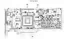
FIG. 1 depicts a bottom side of a printed circuit board comprising a surface mounted layout to reduce voltage noise, according to one embodiment.
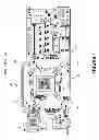
FIG. 2 depicts a top side of the printed circuit board of FIG. 1 comprising a surface mounted high-speed processing unit, according to one embodiment.
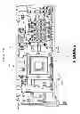
FIG. 3 is a close-up perspective view of the printed circuit board of FIG. 1 comprising a surface mounted layout to reduce voltage noise, according to one embodiment.
FIG. 4 is a circuit diagram depicting a portion of the surface mounted circuit layout of FIG. 1, according to one embodiment.
FIG. 5 is a simplified cross-sectional view depicting the orientation of the printed circuit board layout of FIG. 1, according to one embodiment.
FIG. 6 is a process flow diagram illustrating a method of reducing voltage noise carried by voltage supply lines on a printed circuit board, according to one embodiment.
Other features of the present embodiments will be apparent from the accompanying drawings and from the detailed description that follows.
DETAILED DESCRIPTION
Disclosed are methods and systems to reduce voltage noise on a printed circuit board through a co-layout of multilayer ceramic capacitors. Although the present embodiments have been described with reference to specific example embodiments, it will be evident that various modifications and changes may be made to these embodiments without departing from the broader spirit and scope of the various embodiments.
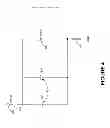
Reference is now made to FIG. 1 which depicts a bottom side of a printed circuit board 100 comprising a surface mounted layout to reduce voltage noise, according to one or more embodiments. Such voltage noise may be the result of spurious oscillations carried by the voltage supply lines or because of interactions between the run-time behavior of software code and the innate characteristics of the underlying power delivery system. For example, parasitic inductance in the power system may cause voltages to fluctuate as current draws change with processor activity. Significant voltage overshoots can cause long-term damage to transistors and other components within an integrated circuit package.
In one embodiment, a surface mounted layout to reduce voltage noise on a printed circuit board 100 comprises a first co-layout of multilayer ceramic capacitors 102 mounted on a first corner of a rectangular footprint 104 of a bottom side 106 of the printed circuit board 100. A co-layout may refer to a functional layout on a printed circuit board where multiple board components (e.g., capacitors, inductors, etc.) are laid out in a substantially parallel configuration that may serve the same purpose as a singular board component of substantially the same functional characteristic. In this embodiment, the co-layout of multilayer ceramic capacitors 102 may refer to two multilayer ceramic capacitors arranged in tandem in substantially the same parallel configuration shown in FIG. 1. The multilayer ceramic capacitors may be surface mounted using typical reflow soldering techniques. It should be understood by one of ordinary skill in the art that a co-layout may also refer to any track routing and circuitry needed to achieve the co-layout described in the present embodiment.
Each of the multilayer ceramic capacitors may comprise of a thin layer of formulated ceramic dielectric sandwiched between metal electrodes alternately exposed on opposite edges of a laminated structure. Such multilayer ceramic capacitors may take the shape of a monolithic block and may comprise a nickel barrier layer and a tin overplate for ease of solderability. Each of the multilayer ceramic capacitors may also have thermal performance limitations (or thermal specifications) of between −55° C. and 125° C.
In this embodiment, the surface mounted layout also comprises a second co-layout of multilayer ceramic capacitors 108 mounted on a second corner of the rectangular footprint 104 of the bottom side 106 of the printed circuit board 100 diagonal to the first corner. In this embodiment, the second co-layout of multilayer ceramic capacitors may comprise of the same multilayer ceramic capacitors used to construct the first co-layout of multilayer ceramic capacitors 102. In the present embodiment, the second co-layout of multilayer ceramic capacitors 108 occupies a second corner of the rectangular footprint 104 that is diagonal to the first co-layout. The term “diagonal” may refer to a position that is directly diagonal to the first corner or substantially diagonal to the first corner. For example, as depicted in FIG. 1, the first co-layout of multilayer ceramic capacitors 102 may be surface mounted on a northwest corner of the rectangular footprint 104 and the second co-layout of multilayer ceramic capacitors 108 may be surface mounted on a southeast corner of the rectangular footprint 104. In another embodiment, the first co-layout of multilayer ceramic capacitors 102 may be surface mounted on a northeast corner of the rectangular footprint 104 and the second co-layout of multilayer ceramic capacitors 108 may be surface mounted on a southwest corner of the rectangular footprint 104.
The surface mounted layout also comprises a first solid electrolytic polymer capacitor 110 and a second solid electrolytic polymer capacitor 112 mounted on the remaining corners, respectively, of the rectangular footprint 104 of the bottom side 106 of the printed circuit board 100. The first solid electrolytic polymer capacitor 110 may be an electrolytic capacitor where the electrolyte is a solid rather than a liquid type electrolyte. In one or more embodiments, the solid electrolyte may be a conductive polymer such as Poly(3,4-ethylenedioxythiophene) or PEDT. Such a capacitor may also include a cathode comprised of aluminum and/or tantalum. In this example embodiment, each of the first and second solid electrolytic polymer capacitors may have a capacitance of 330 μF and an equivalent series resistance (ESR) of 6 mΩ. Such characteristics are important for the capacitors to handle high switching operations and applications involving high ripple currents. Furthermore, each of the solid electrolytic polymer capacitors may withstand operating temperature ranges of between −40° C. and 105° C.
Reference is now made to FIG. 2 which depicts a top side of the printed circuit board of FIG. 1 comprising a surface mounted high-speed processing unit, according to one or more embodiments. As shown in FIG. 2, a high-speed processing unit 200 is surface mounted on a top side 202 of the printed circuit board 100 opposite that of the bottom side comprising the first co-layout of multilayer ceramic capacitors 102 and second co-layout of multiplayer ceramic capacitors 108. In this embodiment, the high-speed processing unit 200 may be a graphics processing unit (GPU) or a central processing unit (CPU). In addition, the printed circuit board 100 may be configured to be integrated into a computer graphics card, a mobile graphics card, a computer video adapter, a mobile video adapter, a computer graphics adapter, and/or a mobile graphics adapter. In one or more embodiments, the computer graphics card may be any of NVIDIA's® GeForce® line of graphics cards, including: the GTX 650® card, the GTX 660® card, the GTX 670® card, the GTX 680® card, and/or the GTX 690® card.
Reference is now made to FIG. 3, which is a close-up perspective view of the printed circuit board of FIG. 1 comprising a surface mounted layout to reduce voltage noise, according to one or more embodiments. As can be seen in FIGS. 1, 2, and 3, the rectangular footprint 104 is a footprint of the high-speed processing unit 200 of FIG. 2 mounted on the top side 202 of the printed circuit board. In this embodiment, the term “footprint” refers to a physical area occupied by an electronic component when mounted on a printed circuit board. In this embodiment, the rectangular footprint 104 may be indicated by a copper pattern etched on the printed circuit board and/or a virtual footprint that is visible only on computer-assisted drawings of the board's layout. In one embodiment, the rectangular footprint may be a footprint of the integrated circuit package containing the high-speed processing unit 200. In one or more embodiments, the rectangular footprint 104 may be substantially a square having side dimensions between 20 and 35 mm. In one embodiment, the first co-layout of multilayer ceramic capacitors 102 may be mounted on a northwest corner of the rectangular footprint 104 and the second co-layout of multilayer ceramic capacitors 108 may be mounted on a southeast corner of the rectangular footprint 104. Additionally, the first solid electrolytic polymer capacitor 110 may be mounted on a northeast corner of the rectangular footprint 104 and the second solid electrolytic polymer capacitor 112 may be mounted on a southwest corner of the rectangular footprint 104.
In another embodiment, the diagonal arrangement may be switched so that the first co-layout of multilayer ceramic capacitors 102 may be mounted on a northeast corner of the rectangular footprint 104 and the second co-layout of multilayer ceramic capacitors 108 may be mounted on a southwest corner of the rectangular footprint 104. In this alternative embodiment, the first solid electrolytic polymer capacitor 110 may be mounted on a northwest corner of the rectangular footprint 104 and the second solid electrolytic polymer capacitor 112 may be mounted on a southeast corner of the rectangular footprint 104. Arranging the capacitor sets diagonally from one another allows a board designer to locate the decoupling capacitors close to the voltage supply pins and ground pins of the high-speed processing unit 200 but does not require any of the capacitors to be located outside the confines of the rectangular footprint 104.
Moreover, the surface mounted layout of FIG. 1 and FIG. 3 allow a board designer to take advantage of the improved thermal specifications of the set of multilayer ceramic capacitors compared with those of their solid electrolytic polymer counterparts. While the multilayer ceramic capacitors used to construct the first and second co-layout of capacitors may have a maximum thermal limitation of 125° C., the solid electrolytic polymers may have a maximum thermal limitation of 105° C. When mounted directly underneath the heat-dissipating high-speed processing unit 200, it may be beneficial to maximize the distance between the two solid electrolytic polymer capacitors so as not to cause either or both of the solid electrolytic polymer capacitors to overheat and surpass the component's thermal specifications. Thus, the corner layout of FIGS. 1 and 3 allow the decoupling mechanism to take advantage of the high capacitance and low ESR of the solid electrolytic polymer capacitors while also maintaining the high thermal integrity of the multilayer ceramic capacitors.
Reference is now made to FIG. 4, which is a circuit diagram depicting a portion of the surface mounted circuit layout of FIG. 1, according to one embodiment. In this embodiment, a set of leads of the first co-layout of multilayer ceramic capacitors 102, the first solid electrolytic polymer capacitor 110, the second co-layout of multilayer ceramic capacitors 108, and/or the second solid electrolytic polymer capacitors 112 is coupled to a voltage supply pin 402 and/or a ground pin 404 of a voltage supply 400 of the high-speed processing unit 200 through a via (see FIG. 5). The voltage supply 400 of the high-speed processing unit 200 may be a core voltage supply and the voltage may be delivered through NVVDD voltage supply lines or rails. In another embodiment, the surface mounted layout of FIG. 1 may be used to reduce voltage noise on other power lines including, but not limited to, DACVDD, PLLVDD, and FBVDD. As shown in FIG. 4, the multilayer ceramic capacitors used to construct either the first co-layout or the second co-layout of multilayer ceramic capacitors may each have a capacitance of 10 μF. In addition, the solid electrolytic polymer capacitor may have a capacitance of 330 μF. In this embodiment, the combination of two 10 μF multilayer ceramic capacitors and one 330 μF may be used to reduce voltage noise at frequencies in the range of 500-600 kHz. In another embodiment, the multilayer ceramic capacitors used to construct either the first co-layout or the second co-layout of multilayer ceramic capacitors may each have a capacitance of 47 μF with the solid electrolytic polymer capacitor maintaining its capacitance of 330 μF. In this alternative embodiment, the combination of two 47 μF multilayer ceramic capacitors and one 330 μF may be used to reduce voltage noise at frequencies in the range of 100-200 kHz.
Reference is now made to FIG. 5, which is a simplified cross-sectional view depicting the orientation of the printed circuit board layout of FIG. 1, according to one embodiment. In this embodiment, the high-speed processing unit 200 is mounted on the top side 202 of the printed circuit board and the co-layout of multilayer ceramic capacitors and the solid electrolytic polymer capacitors are mounted on the bottom side 106 of the printed circuit board 100 directly underneath the high speed processing unit 200. This layout is preferred because the high-speed and high-current nature of logic integrated circuits such as GPUs require capacitors that serve a decoupling purpose to be located in close proximity to the voltage supply pins of such integrated circuits. Since the inductance of the lead-out wires within an IC package often is significant in such cases, the voltage supply and ground pins of the high performance IC must be located in a tight configuration around the chip package. In this case, both the leads of the co-layout of multilayer ceramic capacitors and the solid electrolytic capacitors may be limited to one or more vias 500 between the various circuit layers. In the present embodiment, both the first co-layout of multilayer ceramic capacitors 102 and the second co-layout of multilayer ceramic capacitors 108 and the first and second solid electrolytic polymer capacitors (110 and 112) are mounted within the rectangular footprint 104 of the high-speed processing unit 200. Moreover, the diagonal arrangement of such capacitors allows for improved connections between the leads of the capacitors and the various supply and ground pins of the high-speed processor.
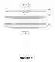
FIG. 6 is a process flow diagram illustrating a method of reducing voltage noise carried by voltage supply lines (e.g., NVVDD rails) on a printed circuit board, according to one embodiment. In one embodiment, operation 600 may involve surface mounting a first co-layout of multilayer ceramic capacitors 102 on a first corner of a rectangular footprint 104 of a bottom side 106 of the printed circuit board 100. The first co-layout of multilayer ceramic capacitors 102 may be mounted on the printed circuit board 100 using any commonly developed surface mounted soldering techniques, including reflow soldering. In addition, operation 602 may involve surface mounting a second co-layout of multilayer capacitors 108 on a second corner of the rectangular footprint 104 of the bottom side 106 of the printed circuit board 100. The second corner of the rectangular footprint of the printed circuit board may be substantially diagonal to the first corner of the rectangular footprint of the printed circuit board. Furthermore, operation 604 may involve surface mounting a first solid electrolytic polymer capacitor 110 and a second solid electrolytic polymer capacitor 112 on the remaining corners, respectively, of the rectangular footprint 104 of the bottom side 106 of the printed circuit board 100. In this embodiment, a high-speed processing unit 200 is surface mounted on a top side 202 of the printed circuit board 100 opposite that of the bottom side 106.
Although the present embodiments have been described with reference to specific example embodiments, it will be evident that various modifications and changes may be made to these embodiments without departing from the broader spirit and scope of the various embodiments. For example, the surface mounted layout may be expressed as an electronic assembly comprising the surface mounted layout and both the surface mounted layout and the electronic assembly may be integrated into any of a computer graphics card, a mobile graphics card, a computer video adapter, a mobile video adapter, a computer graphics adapter, and/or a mobile graphics adapter.
Claims
What is claimed is:1. A surface mounted layout to reduce voltage noise on a printed circuit board, comprising:
a first co-layout of multilayer ceramic capacitors mounted on a first corner of a rectangular footprint of a bottom side of the printed circuit board;
a second co-layout of multilayer ceramic capacitors mounted on a second corner of the rectangular footprint of the bottom side of the printed circuit board diagonal to the first corner; and
a first solid electrolytic polymer capacitor and a second solid electrolytic polymer capacitor mounted on the remaining corners, respectively, of the rectangular footprint of the bottom side of the printed circuit board,
wherein the rectangular footprint of the printed circuit board is a footprint of a high-speed processing unit mounted on the printed circuit board, and
wherein the high-speed processing unit is mounted on a top side of the printed circuit board opposite the bottom side comprising the first co-layout of multilayer ceramic capacitors and the second co-layout of multilayer ceramic capacitors, and
wherein a set of leads of at least one of the first co-layout of multilayer ceramic capacitors, the first solid electrolytic polymer capacitor, the second co-layout of multilayer ceramic capacitors, and the second solid electrolytic polymer capacitor is coupled to at least one of a voltage supply pin and a ground pin of a voltage supply of the high-speed processing unit through a via.
2. The surface mounted layout of claim 1, wherein the high-speed processing unit is at least one of a central processing unit (CPU) and a graphics processing unit (GPU).
3. The surface mounted layout of claim 1, wherein the voltage supply of the high-speed processing unit is at least one of an NVVDD and a core voltage of the high-speed processing unit.
4. The surface mounted layout of claim 1, wherein the rectangular footprint is substantially a square having a side dimension between 20 and 35 mm.
5. The surface mounted layout of claim 1, wherein a set of thermal performance limitations for each of the multilayer ceramic capacitors is between −55° C. and 125° C. and a set of thermal performance limitations for each of the first solid electrolytic polymer capacitor and the second solid electrolytic polymer capacitor is between −40° C. and 105° C.
6. The surface mounted layout of claim 1, wherein each of the multilayer ceramic capacitors has a capacitance of 10 μF.
7. The surface mounted layout of claim 1, wherein each of the multilayer ceramic capacitors has a capacitance of 47 μF.
8. The surface mounted layout of claim 1, wherein the printed circuit board is configured to be integrated into at least one of a computer graphics card, a mobile graphics card, a computer video adapter, a mobile video adapter, a computer graphics adapter, and a mobile graphics adapter.
9. An electronic assembly to reduce voltage noise, comprising:
a first co-layout of multilayer ceramic capacitors surface mounted on a first corner of a rectangular footprint of a bottom side of the printed circuit board;
a second co-layout of multilayer ceramic capacitors surface mounted on a second corner of the rectangular footprint of the bottom side of the printed circuit board diagonal to the first corner; and
a first solid electrolytic polymer capacitor and a second solid electrolytic polymer capacitor surface mounted on the remaining corners, respectively, of the rectangular footprint of the bottom side of the printed circuit board,
wherein the rectangular footprint of the printed circuit board is a footprint of a high-speed processing unit mounted on the printed circuit board,
wherein the high-speed processing unit is surface mounted on a top side of the printed circuit board opposite that of the bottom side comprising the first co-layout of multilayer ceramic capacitors and the second co-layout of multilayer ceramic capacitors, and
wherein a set of leads of at least one of the first co-layout of multilayer ceramic capacitors, the first solid electrolytic polymer capacitor, the second co-layout of multilayer ceramic capacitors, and the second solid electrolytic polymer capacitor is coupled to at least one of a voltage supply pin and a ground pin of a voltage supply of the high-speed processing unit through a via.
10. The electronic assembly of claim 9, wherein the high-speed processing unit is at least one of a central processing unit (CPU) and a graphics processing unit (GPU).
11. The electronic assembly of claim 9, wherein the voltage supply of the high-speed processing unit is at least one of an NVVDD and a core voltage of the high-speed processing unit.
12. The electronic assembly of claim 9, wherein the rectangular footprint is substantially a square having a side dimension between 20 and 35 mm.
13. The electronic assembly of claim 9, wherein a set of thermal performance limitations for each of the multilayer ceramic capacitors is between −55° C. and 125° C. and a set of thermal performance limitations for each of the first solid electrolytic polymer capacitor and the second solid electrolytic polymer capacitor is between −40° C. and 105° C.
14. The electronic assembly of claim 9, wherein each of the multilayer ceramic capacitors has a capacitance of 10 μF.
15. The electronic assembly of claim 9, wherein each of the multilayer ceramic capacitors has a capacitance of 47 μF.
16. The electronic assembly of claim 9, wherein the printed circuit board is configured to be integrated into at least one of a computer graphics card, a mobile graphics card, a computer video adapter, a mobile video adapter, a computer graphics adapter, and a mobile graphics adapter.
17. A method of assembling a printed circuit board to reduce voltage noise, comprising:
surface mounting on a first corner of a rectangular footprint of a bottom side of the printed circuit board a first co-layout of multilayer ceramic capacitors;
surface mounting on a second corner of the rectangular footprint of the bottom side of the printed circuit board diagonal to the first corner a second co-layout of multilayer ceramic capacitors; and
surface mounting on the remaining corners, respectively, of the rectangular footprint of the bottom side of the printed circuit board a first solid electrolytic polymer capacitor and a second solid electrolytic polymer capacitor,
wherein the rectangular footprint of the printed circuit board is a footprint of a high-speed processing unit mounted on the printed circuit board,
wherein the high-speed processing unit is surface mounted on a top side of the printed circuit board opposite the bottom side comprising the first co-layout of multilayer ceramic capacitors and the second co-layout of multilayer ceramic capacitors,
wherein a set of leads of at least one of the first co-layout of multilayer ceramic capacitors, the first solid electrolytic polymer capacitor, the second co-layout of multilayer ceramic capacitors, and the second solid electrolytic polymer capacitor is coupled to at least one of a voltage supply pin and a ground pin of a voltage supply of the high-speed processing unit through a via, and
wherein the voltage supply of the high-speed processing unit is at least one of an NVVDD and a core voltage of the high-speed processing unit.
18. The method of claim 17, wherein the high-speed processing unit is at least one of a central processing unit (CPU) and a graphics processing unit (GPU) and the rectangular footprint is substantially a square having a side dimension between 20 and 35 mm.
19. The method of claim 17, wherein a set of thermal performance limitations for each of the multilayer ceramic capacitors is between −55° C. and 125° C. and a set of thermal performance limitations for each of the first solid electrolytic polymer capacitor and the second solid electrolytic polymer capacitor is between −40° C. and 105° C. and each of the multilayer ceramic capacitors has a capacitance of 47 μF.
20. The method of claim 17, wherein the printed circuit board is configured to be integrated into at least one of a computer graphics card, a mobile graphics card, a computer video adapter, a mobile video adapter, a computer graphics adapter, and a mobile graphics adapter.
Images & Drawings included:
Sources:
- United States Patent and Trademark Office - verify current appl. status at the USPTO↗
Recent applications in this class:
- » 20250138578 2025-05-01
ELECTRONIC DEVICE - » 20250004497 2025-01-02
Tablet Protective Case and Tablet Keyboard Kit - » 20240353893 2024-10-24
Front Port Dongle for a Server Type Information Handling System - » 20240353892 2024-10-24
Information Handling System with Retractable Input/Output Port Component - » 20220163995 2022-05-26
METHOD AND SYSTEM FOR ADJUSTABLE HEIGHT KIOSK - » 20220155816 2022-05-19
DEVICES AND METHODS FOR DISPENSING HAND SANITIZER - » 20210286401 2021-09-16
Touch-sensitive screen - » 20210132651 2021-05-06
Shakeproof modular computer system - » 20210103312 2021-04-08
Structure of electronic device and electronic device - » 20210034097 2021-02-04
Universal bracket for multiple form factors of PCIe cards in OCP sled environments
Recent applications for this Assignee:
- » 20250292497 2025-09-18
MACHINE LEARNING MODELS FOR RECONSTRUCTION AND SYNTHESIS OF DYNAMIC SCENES FROM VIDEO - » 20250292137 2025-09-18
HYBRID QUANTUM-CLASSICAL SYSTEM FOR ENHANCED COMBINATORIAL OPTIMIZATION - » 20250284618 2025-09-11
HEALTH AND ERROR MONITORING OF SENSOR FUSION SYSTEMS - » 20250271576 2025-08-28
THREE-DIMENSIONAL (3D) OBJECT DETECTION AND LABELING USING MOTION CUES - » 20250264528 2025-08-21
Test Data Transfer in Multi-Die Systems - » 20250258683 2025-08-14
FINITE STATE MACHINES WITH MULTI-STATE RECONCILIATION IN DISTRIBUTED COMPUTING INFRASTRUCTURES - » 20250244807 2025-07-31
SYSTEMS AND METHODS FOR TEMPERATURE REGULATION OF ELECTRONIC DEVICES - » 20250234459 2025-07-17
CHIP-TO-CHIP INTERCONNECT DESIGN - » 20250232505 2025-07-17
MACHINE LEARNING MODELS FOR GENERATIVE HUMAN MOTION SIMULATION - » 20250232504 2025-07-17
MACHINE LEARNING MODELS FOR GENERATIVE HUMAN MOTION SIMULATION