Miniaturized SMD diode package and process for producing the same
US20150200147A1
2015-07-16
14/585,857
2014-12-30
✅ Patent granted
US 9,691,735 B2
2017-06-27
-
-
Thao X Le | Nduka Ojeh
Bacon & Thomas, PLLC
2034-12-30
Abstract:
A miniaturized SMD diode package involves using a diode chip whose bottom surface has a positive electrode and a negative electrode, using a circuit board instead of a conventional lead frame during packaging, and using Charge-Coupled Device (CCD) image registration technology to perform chip bonding; the beneficial advantages brought from a process for producing the same including to simplify producing process and reduce manufacturing cost, to improve accuracy and precision of producing the miniaturized SMD diode package due to using a circuit board instead of conventionally used lead frame, and to ensure the produced miniaturized SMD diode package possesses excellent diode characteristics without distortion or defect.
Inventors:
- Ching-Hohn LIEN 4 🇹🇼 Taoyuan County, Taiwan
- Xing- Xiang HUANG 3 🇹🇼 Taoyuan County, Taiwan
- Hsing-Tsai HUANG 3 🇹🇼 Taoyuan County, Taiwan
- Hong-Zong XU 3 🇹🇼 Taoyuan County, Taiwan
- Yi-Wei CHEN 2 🇹🇼 Taoyuan County, Taiwan
Assignee:
- SFI Electronics Technology Inc. 3 🇹🇼 , Taiwan
Applicant:
Interested in similar patents?
Get notified when new applications in this technology area are published.
Classification:
H01L2924/1203 » CPC further
Indexing scheme for arrangements or methods for connecting or disconnecting semiconductor or solid-state bodies as covered by; Details of semiconductor or other solid state devices to be connected; Device type; Passive devices, e.g. 2 terminal devices Rectifying Diode
H01L23/00 IPC
Details of semiconductor or other solid state devices
H01L21/56 » CPC further
Processes or apparatus adapted for the manufacture or treatment of semiconductor or solid state devices or of parts thereof; Manufacture or treatment of semiconductor devices or of parts thereof the devices having at least one potential-jump barrier or surface barrier, e.g. PN junction, depletion layer or carrier concentration layer; Assembly of semiconductor devices using processes or apparatus not provided for in a single one of the subgroups - , e.g. sealing of a cap to a base of a container Encapsulations, e.g. encapsulation layers, coatings
H01L21/78 » CPC further
Processes or apparatus adapted for the manufacture or treatment of semiconductor or solid state devices or of parts thereof; Manufacture or treatment of devices consisting of a plurality of solid state components formed in or on a common substrate or of parts thereof; Manufacture of integrated circuit devices or of parts thereof; Manufacture or treatment of devices consisting of a plurality of solid state components or integrated circuits formed in, or on, a common substrate with subsequent division of the substrate into plural individual devices
H01L23/02 » CPC further
Details of semiconductor or other solid state devices Containers; Seals
H01L23/15 » CPC main
Details of semiconductor or other solid state devices; Mountings, e.g. non-detachable insulating substrates characterised by the material or its electrical properties Ceramic or glass substrates
H01L23/31 IPC
Details of semiconductor or other solid state devices; Encapsulations, e.g. encapsulating layers, coatings, e.g. for protection characterised by the arrangement or shape
H01L23/3107 » CPC further
Details of semiconductor or other solid state devices; Encapsulations, e.g. encapsulating layers, coatings, e.g. for protection characterised by the arrangement or shape the device being completely enclosed
H01L29/861 » CPC further
Semiconductor devices adapted for rectifying, amplifying, oscillating or switching, or capacitors or resistors with at least one potential-jump barrier or surface barrier, e.g. PN junction depletion layer or carrier concentration layer; Details of semiconductor bodies or of electrodes thereof; Multistep manufacturing processes therefor; Types of semiconductor device ; Multistep manufacturing processes therefor controllable only by variation of the electric current supplied, or only the electric potential applied, to one or more of the electrodes carrying the current to be rectified, amplified, oscillated or switched Diodes
H01L24/83 » CPC further
Arrangements for connecting or disconnecting semiconductor or solid-state bodies; Methods or apparatus related thereto; Methods for connecting semiconductor or other solid state bodies using means for bonding being attached to, or being formed on, the surface to be connected using a layer connector
H01L24/97 » CPC main
Arrangements for connecting or disconnecting semiconductor or solid-state bodies; Methods or apparatus related thereto; Batch processes at chip-level, i.e. with connecting carried out on a plurality of singulated devices, i.e. on diced chips the devices being connected to a common substrate, e.g. interposer, said common substrate being separable into individual assemblies after connecting
H01L21/4867 » CPC further
Processes or apparatus adapted for the manufacture or treatment of semiconductor or solid state devices or of parts thereof; Manufacture or treatment of semiconductor devices or of parts thereof the devices having at least one potential-jump barrier or surface barrier, e.g. PN junction, depletion layer or carrier concentration layer; Manufacture or treatment of parts, e.g. containers, prior to assembly of the devices, using processes not provided for in a single one of the subgroups -; Conductive parts; Leads on or in insulating or insulated substrates, e.g. metallisation Applying pastes or inks, e.g. screen printing
H01L21/561 » CPC further
Processes or apparatus adapted for the manufacture or treatment of semiconductor or solid state devices or of parts thereof; Manufacture or treatment of semiconductor devices or of parts thereof the devices having at least one potential-jump barrier or surface barrier, e.g. PN junction, depletion layer or carrier concentration layer; Assembly of semiconductor devices using processes or apparatus not provided for in a single one of the subgroups - , e.g. sealing of a cap to a base of a container; Encapsulations, e.g. encapsulation layers, coatings Batch processing
H01L21/565 » CPC further
Processes or apparatus adapted for the manufacture or treatment of semiconductor or solid state devices or of parts thereof; Manufacture or treatment of semiconductor devices or of parts thereof the devices having at least one potential-jump barrier or surface barrier, e.g. PN junction, depletion layer or carrier concentration layer; Assembly of semiconductor devices using processes or apparatus not provided for in a single one of the subgroups - , e.g. sealing of a cap to a base of a container; Encapsulations, e.g. encapsulation layers, coatings Moulds
H01L23/49805 » CPC further
Details of semiconductor or other solid state devices; Arrangements for conducting electric current to or from the solid state body in operation, e.g. leads, terminal arrangements ; Selection of materials therefor consisting of soldered constructions; Leads, on insulating substrates, the leads being also applied on the sidewalls or the bottom of the substrate, e.g. leadless packages for surface mounting
H01L23/49833 » CPC further
Details of semiconductor or other solid state devices; Arrangements for conducting electric current to or from the solid state body in operation, e.g. leads, terminal arrangements ; Selection of materials therefor consisting of soldered constructions; Leads, on insulating substrates, the chip support structure consisting of a plurality of insulating substrates
H05K1/144 » CPC further
Printed circuits; Details; Structural association of two or more printed circuits Stacked arrangements of planar printed circuit boards
H05K1/144 » CPC further
Printed circuits; Details; Structural association of two or more printed circuits Stacked arrangements of planar printed circuit boards
H05K1/145 » CPC further
Printed circuits; Details; Structural association of two or more printed circuits Arrangements wherein electric components are disposed between and simultaneously connected to two planar printed circuit boards, e.g. Cordwood modules
H05K1/145 » CPC further
Printed circuits; Details; Structural association of two or more printed circuits Arrangements wherein electric components are disposed between and simultaneously connected to two planar printed circuit boards, e.g. Cordwood modules
H05K3/403 » CPC further
Apparatus or processes for manufacturing printed circuits; Forming printed elements for providing electric connections to or between printed circuits Edge contacts; Windows or holes in the substrate having plural connections on the walls thereof
H05K3/403 » CPC further
Apparatus or processes for manufacturing printed circuits; Forming printed elements for providing electric connections to or between printed circuits Edge contacts; Windows or holes in the substrate having plural connections on the walls thereof
H01L24/27 » CPC further
Arrangements for connecting or disconnecting semiconductor or solid-state bodies; Methods or apparatus related thereto; Means for bonding being attached to, or being formed on, the surface to be connected, e.g. chip-to-package, die-attach, "first-level" interconnects; Manufacturing methods related thereto; Layer connectors, e.g. plate connectors, solder or adhesive layers; Manufacturing methods related thereto Manufacturing methods
H01L24/29 » CPC further
Arrangements for connecting or disconnecting semiconductor or solid-state bodies; Methods or apparatus related thereto; Means for bonding being attached to, or being formed on, the surface to be connected, e.g. chip-to-package, die-attach, "first-level" interconnects; Manufacturing methods related thereto; Layer connectors, e.g. plate connectors, solder or adhesive layers; Manufacturing methods related thereto; Structure, shape, material or disposition of the layer connectors prior to the connecting process of an individual layer connector
H01L24/32 » CPC further
Arrangements for connecting or disconnecting semiconductor or solid-state bodies; Methods or apparatus related thereto; Means for bonding being attached to, or being formed on, the surface to be connected, e.g. chip-to-package, die-attach, "first-level" interconnects; Manufacturing methods related thereto; Layer connectors, e.g. plate connectors, solder or adhesive layers; Manufacturing methods related thereto; Structure, shape, material or disposition of the layer connectors after the connecting process of an individual layer connector
H01L24/33 » CPC further
Arrangements for connecting or disconnecting semiconductor or solid-state bodies; Methods or apparatus related thereto; Means for bonding being attached to, or being formed on, the surface to be connected, e.g. chip-to-package, die-attach, "first-level" interconnects; Manufacturing methods related thereto; Layer connectors, e.g. plate connectors, solder or adhesive layers; Manufacturing methods related thereto; Structure, shape, material or disposition of the layer connectors after the connecting process of a plurality of layer connectors
H01L25/0652 » CPC further
Assemblies consisting of a plurality of individual semiconductor or other solid state devices ; Multistep manufacturing processes thereof all the devices being of a type provided for in the same subgroup of groups - , e.g. assemblies of rectifier diodes the devices not having separate containers the devices being of a type provided for in group the devices being arranged next and on each other, i.e. mixed assemblies
H01L2224/2732 » CPC further
Indexing scheme for arrangements for connecting or disconnecting semiconductor or solid-state bodies and methods related thereto as covered by; Means for bonding being attached to, or being formed on, the surface to be connected, e.g. chip-to-package, die-attach, "first-level" interconnects; Manufacturing methods related thereto; Layer connectors, e.g. plate connectors, solder or adhesive layers; Manufacturing methods related thereto; Manufacturing methods by local deposition of the material of the layer connector in liquid form Screen printing, i.e. using a stencil
H01L2224/27312 » CPC further
Indexing scheme for arrangements for connecting or disconnecting semiconductor or solid-state bodies and methods related thereto as covered by; Means for bonding being attached to, or being formed on, the surface to be connected, e.g. chip-to-package, die-attach, "first-level" interconnects; Manufacturing methods related thereto; Layer connectors, e.g. plate connectors, solder or adhesive layers; Manufacturing methods related thereto; Manufacturing methods by local deposition of the material of the layer connector in liquid form Continuous flow, e.g. using a microsyringe, a pump, a nozzle or extrusion
H01L2224/83101 » CPC further
Indexing scheme for arrangements for connecting or disconnecting semiconductor or solid-state bodies and methods related thereto as covered by; Methods for connecting semiconductor or other solid state bodies using means for bonding being attached to, or being formed on, the surface to be connected using a layer connector the layer connector being supplied to the parts to be connected in the bonding apparatus as prepeg comprising a layer connector, e.g. provided in an insulating plate member
H01L2224/83191 » CPC further
Indexing scheme for arrangements for connecting or disconnecting semiconductor or solid-state bodies and methods related thereto as covered by; Methods for connecting semiconductor or other solid state bodies using means for bonding being attached to, or being formed on, the surface to be connected using a layer connector; Arrangement of the layer connectors prior to mounting wherein the layer connectors are disposed only on the semiconductor or solid-state body
H01L2224/83192 » CPC further
Indexing scheme for arrangements for connecting or disconnecting semiconductor or solid-state bodies and methods related thereto as covered by; Methods for connecting semiconductor or other solid state bodies using means for bonding being attached to, or being formed on, the surface to be connected using a layer connector; Arrangement of the layer connectors prior to mounting wherein the layer connectors are disposed only on another item or body to be connected to the semiconductor or solid-state body
H01L2224/83801 » CPC further
Indexing scheme for arrangements for connecting or disconnecting semiconductor or solid-state bodies and methods related thereto as covered by; Methods for connecting semiconductor or other solid state bodies using means for bonding being attached to, or being formed on, the surface to be connected using a layer connector; Bonding techniques Soldering or alloying
H01L2224/83851 » CPC further
Indexing scheme for arrangements for connecting or disconnecting semiconductor or solid-state bodies and methods related thereto as covered by; Methods for connecting semiconductor or other solid state bodies using means for bonding being attached to, or being formed on, the surface to be connected using a layer connector; Bonding techniques using a polymer adhesive, e.g. an adhesive based on silicone, epoxy, polyimide, polyester being an anisotropic conductive adhesive
H01L2224/92 » CPC further
Indexing scheme for arrangements for connecting or disconnecting semiconductor or solid-state bodies and methods related thereto as covered by; Methods for connecting semiconductor or solid state bodies including different methods provided for in two or more of groups - Specific sequence of method steps
H01L2224/97 » CPC further
Indexing scheme for arrangements for connecting or disconnecting semiconductor or solid-state bodies and methods related thereto as covered by; Batch processes at chip-level, i.e. with connecting carried out on a plurality of singulated devices, i.e. on diced chips the devices being connected to a common substrate, e.g. interposer, said common substrate being separable into individual assemblies after connecting
H01L2924/12035 » CPC further
Indexing scheme for arrangements or methods for connecting or disconnecting semiconductor or solid-state bodies as covered by; Details of semiconductor or other solid state devices to be connected; Device type; Passive devices, e.g. 2 terminal devices; Rectifying Diode Zener diode
H01L2924/1579 » CPC further
Indexing scheme for arrangements or methods for connecting or disconnecting semiconductor or solid-state bodies as covered by; Details of package parts other than the semiconductor or other solid state devices to be connected; Die mounting substrate; Material with a principal constituent of the material being a polymer, e.g. polyester, phenolic based polymer, epoxy
H01L2924/15787 » CPC further
Indexing scheme for arrangements or methods for connecting or disconnecting semiconductor or solid-state bodies as covered by; Details of package parts other than the semiconductor or other solid state devices to be connected; Die mounting substrate; Material with a principal constituent of the material being a non metallic, non metalloid inorganic material Ceramics, e.g. crystalline carbides, nitrides or oxides
H01L2924/15798 » CPC further
Indexing scheme for arrangements or methods for connecting or disconnecting semiconductor or solid-state bodies as covered by; Details of package parts other than the semiconductor or other solid state devices to be connected; Die mounting substrate; Material with a principal constituent of the material being a combination of two or more materials in the form of a matrix with a filler, i.e. being a hybrid material, e.g. segmented structures, foams
H01L2924/181 » CPC further
Indexing scheme for arrangements or methods for connecting or disconnecting semiconductor or solid-state bodies as covered by; Details of package parts other than the semiconductor or other solid state devices to be connected Encapsulation
H01L2924/186 » CPC further
Indexing scheme for arrangements or methods for connecting or disconnecting semiconductor or solid-state bodies as covered by; Details of package parts other than the semiconductor or other solid state devices to be connected; Encapsulation Material
H01L27/15 IPC
Devices consisting of a plurality of semiconductor or other solid-state components formed in or on a common substrate including semiconductor components with at least one potential-jump barrier or surface barrier specially adapted for light emission
H01L29/267 IPC
Semiconductor devices adapted for rectifying, amplifying, oscillating or switching, or capacitors or resistors with at least one potential-jump barrier or surface barrier, e.g. PN junction depletion layer or carrier concentration layer; Details of semiconductor bodies or of electrodes thereof; Multistep manufacturing processes therefor; Semiconductor bodies ; Multistep manufacturing processes therefor characterised by the materials of which they are formed including, apart from doping materials or other impurities, elements provided for in two or more of the groups , , , , , e.g. alloys in different semiconductor regions, e.g. heterojunctions
H01L31/12 IPC
Semiconductor devices sensitive to infra-red radiation, light, electromagnetic radiation of shorter wavelength or corpuscular radiation and specially adapted either for the conversion of the energy of such radiation into electrical energy or for the control of electrical energy by such radiation; Processes or apparatus specially adapted for the manufacture or treatment thereof or of parts thereof; Details thereof structurally associated with, e.g. formed in or on a common substrate with, one or more electric light sources, e.g. electroluminescent light sources, and electrically or optically coupled thereto
H01L23/498 IPC
Details of semiconductor or other solid state devices; Arrangements for conducting electric current to or from the solid state body in operation, e.g. leads, terminal arrangements ; Selection of materials therefor consisting of soldered constructions Leads, on insulating substrates,
H01L21/48 IPC
Processes or apparatus adapted for the manufacture or treatment of semiconductor or solid state devices or of parts thereof; Manufacture or treatment of semiconductor devices or of parts thereof the devices having at least one potential-jump barrier or surface barrier, e.g. PN junction, depletion layer or carrier concentration layer Manufacture or treatment of parts, e.g. containers, prior to assembly of the devices, using processes not provided for in a single one of the subgroups -
H05K1/11 IPC
Printed circuits; Details Printed elements for providing electric connections to or between printed circuits
H05K1/11 IPC
Printed circuits; Details Printed elements for providing electric connections to or between printed circuits
H05K1/14 IPC
Printed circuits; Details Structural association of two or more printed circuits
H05K1/14 IPC
Printed circuits; Details Structural association of two or more printed circuits
H05K3/40 IPC
Apparatus or processes for manufacturing printed circuits Forming printed elements for providing electric connections to or between printed circuits
H05K3/40 IPC
Apparatus or processes for manufacturing printed circuits Forming printed elements for providing electric connections to or between printed circuits
H01L25/065 IPC
Assemblies consisting of a plurality of individual semiconductor or other solid state devices ; Multistep manufacturing processes thereof all the devices being of a type provided for in the same subgroup of groups - , e.g. assemblies of rectifier diodes the devices not having separate containers the devices being of a type provided for in group
H05K1/117 » CPC further
Printed circuits; Details; Printed elements for providing electric connections to or between printed circuits Pads along the edge of rigid circuit boards, e.g. for pluggable connectors
H05K1/117 » CPC further
Printed circuits; Details; Printed elements for providing electric connections to or between printed circuits Pads along the edge of rigid circuit boards, e.g. for pluggable connectors
H01L2924/12032 » CPC further
Indexing scheme for arrangements or methods for connecting or disconnecting semiconductor or solid-state bodies as covered by; Details of semiconductor or other solid state devices to be connected; Device type; Passive devices, e.g. 2 terminal devices; Rectifying Diode Schottky diode
H01L21/4853 » CPC further
Processes or apparatus adapted for the manufacture or treatment of semiconductor or solid state devices or of parts thereof; Manufacture or treatment of semiconductor devices or of parts thereof the devices having at least one potential-jump barrier or surface barrier, e.g. PN junction, depletion layer or carrier concentration layer; Manufacture or treatment of parts, e.g. containers, prior to assembly of the devices, using processes not provided for in a single one of the subgroups -; Conductive parts; Leads on or in insulating or insulated substrates, e.g. metallisation Connection or disconnection of other leads to or from a metallisation, e.g. pins, wires, bumps
H01L24/96 » CPC further
Arrangements for connecting or disconnecting semiconductor or solid-state bodies; Methods or apparatus related thereto; Batch processes at chip-level, i.e. with connecting carried out on a plurality of singulated devices, i.e. on diced chips the devices being encapsulated in a common layer, e.g. neo-wafer or pseudo-wafer, said common layer being separable into individual assemblies after connecting
H01L2924/12036 » CPC further
Indexing scheme for arrangements or methods for connecting or disconnecting semiconductor or solid-state bodies as covered by; Details of semiconductor or other solid state devices to be connected; Device type; Passive devices, e.g. 2 terminal devices; Rectifying Diode PN diode
Description
BACKGROUND OF THE PRESENT INVENTION
1. Field of the Invention
The present invention relates to surface-mount device (SMD) diode packages, and more particularly to a miniaturized SMD diode package having a circuit board used instead of a conventional lead frame, and a process for producing the same.
2. Description of Related Art
In a given process for making IC or semiconductor packages (or called IC devices), lead frames are conventionally used to hold IC or semiconductor dies (or called IC chips) and further make an electrical connection with the IC chips before performing package of epoxy resin and formed as IC devices.
The lead frame after packaged acts as an inner electrode for the IC devices and further has pins (or contacting points) exposed outside to be worked as outer electrodes for the same IC devices. Therefore, IC device can be connected to a printed circuit board (PCB) via outer electrodes formed from so-called lead frame and to transmit workable functions from IC chips to the PCB, and vice versa.
Accordingly, a lead frame is an essential element for packaging IC chips. Depending on IC chips possessing what function, usage, shape and/or size, various different lead frames are designed for use in packaging those IC chips.
To take a miniaturized SMD diode package as an example, since a miniaturized diode package has a package size like chip scale, it is hardly to allow miniaturized diode chips are accurately and precisely installed on so-called lead frame. The inevitable problem is that a miniaturized diode package leads to have distortion and even failure if inaccurately packaged with lead frames for diode chips.
Therefore, the conventional packaging method that uses lead frames acted as inner electrodes and also as outer electrodes for diode chips do not suitably apply for use in producing the miniaturized SMD diode package.
SUMMARY OF THE INVENTION
In view of this, for improving the existing packaging process for miniaturized SMD diode packages, the present invention discloses a process for producing miniaturized SMD diode packages involves using a diode chip whose bottom surface has a positive electrode and a negative electrode, using a circuit board instead of a conventional lead frame during packaging, and using Charge-Coupled Device (CCD) image registration technology to perform chip bonding.
The beneficial advantages brought from the disclosed process for producing miniaturized SMD diode packages include:
- 1. to simplify producing process and reduce manufacturing cost;
- 2. to improve accuracy and precision of producing the miniaturized SMD diode package due to using a circuit board instead of the conventionally used lead frame;
- 3. to ensure the produced miniaturized SMD diode package possesses excellent diode characteristics without distortion or defect; and
- 4. to produce increasingly miniaturized SMD electronic devices more suitable.
BRIEF DESCRIPTION OF THE DRAWINGS
FIG. 1 is a schematic drawing showing a SMD diode chip package of the present invention.
FIG. 2 is a schematic drawing showing another embodiment of an array-type SMD diode chip package of the present invention.
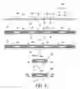
FIG. 3 depicts the SMD diode chip package of FIG. 1 or FIG. 2 in the course of packaging process using a circuit board instead of the conventionally used lead frame to make electrical connections with one or more diodes chips.
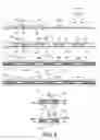
FIG. 4 is a flowchart for producing a first or second embodiment of SMD diode chip package of the present invention.
FIG. 5 is an illustrating drawing to show how to produce a first embodiment of SMD diode chip package of the present invention.
FIG. 6 is an illustrating drawing to show how to produce a second embodiment of SMD diode chip package of the present invention.
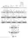
FIG. 7 is a flowchart for producing a third or fourth embodiment of SMD diode chip package of the present invention.
FIG. 8 is an illustrating drawing to show how to produce a third embodiment of SMD diode chip package of the present invention.
FIG. 9 is an illustrating drawing to show how to produce a fourth embodiment of SMD diode chip package of the present invention.
DETAILED DESCRIPTION OF THE INVENTION
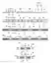
Referred to FIGS. 1 and 3, a SMD diode chip package 10 of the present invention is herein defined as a diode package miniaturized in whole package size like chip scale and having two ends formed with outer electrodes 80a, 80b respectively.
The SMD diode chip package 10 is packaged with a single diode chip 30 and has three basic features including: using a circuit board instead of the conventionally used lead frame, containing no outer pins extended from the so-called lead frame, and possessing excellent diode characteristics.
The SMD diode chip package 10 of the present invention contains four embodiments described as follows.
Referred to FIGS. 1, 3 and 5, formed as a first embodiment of the present invention, a diode package 10a is composed of a diode chip 30a, a bottom circuit board 50, two circuit electrodes 56a, 56b, an encapsulation 75 and two outer electrodes 80a, 80b.
The diode chip 30a for having function of electrical connection has its bottom surface provided with two lower electrodes 31 acting as a positive electrode and a negative electrode, respectively.
The circuit electrodes 56a, 56b are separately deposited on the bottom circuit board 50, and each corresponds to and electrically connects to the corresponding lower electrode 31 of the diode chip 30a, respectively.
The encapsulation 75 is attached to the bottom circuit board 50 and integrated with the bottom circuit board 50 as an integrated structure, so that the diode chip 30a and the circuit electrodes 56a, 56b are contained therein, and the circuit electrodes 56a, 56b each have one end extended to and exposed at one end of the encapsulation 75.
The outer electrodes 80a, 80b each cover one end of the integrated structure formed by the encapsulation 75 and the bottom circuit board 50, and each are electrically connected to the corresponding circuit electrode 56a, 56b, respectively.
Referred to FIG. 6, formed as a second embodiment of the present invention, a diode package 10b comprises all basic structures presented on the aforesaid diode package 10a, and further has an upper cover 53 that is attached to a top surface of the encapsulation 75 and forms an integrated structure together with the encapsulation 75 and the bottom circuit board 50.
Accordingly, the outer electrodes 80a, 80b each cover one end of the integrated structure formed by the upper cover 53, the encapsulation 75 and the bottom circuit board 50, and each are electrically connected to the corresponding circuit electrode 56a, 56b, respectively.
Referred to FIGS. 1, 3 and 8, formed as a third embodiment of the present invention, a diode package 10c is composed of a diode chip 30b having three electrodes, a bottom circuit board 50, two circuit electrodes 56a, 56b, a top circuit board 60, an upper circuit electrode 66a, an encapsulation 75 and two outer electrodes 80a, 80b.
The diode chip 30b for increasing current capacity has its bottom surface provided with two lower electrodes 31 acting as a positive electrode and a negative electrode respectively, and has its top surface provided with a higher electrode 32 acting as a positive electrode or a negative electrode.
The circuit electrodes 56a, 56b are separately deposited on the bottom circuit board 50, and each corresponds to and electrically connects to the corresponding lower electrode 31 of the diode chip 30b, respectively.
The upper circuit electrode 66a is deposited on the top circuit board 60, and corresponds to and electrically connects to the higher electrode 32 of the diode chip 30b.
The encapsulation 75 is attached between the bottom circuit board 50 and the top circuit board 60 as well as integrated with them as an integrated structure, so that the diode chip 30b, the circuit electrodes 56a, 56b and the upper circuit electrode 66a are all contained therein, and the circuit electrodes 56a, 56b and the upper circuit electrode 66a each have one end extended to and exposed at one end of the encapsulation 75.
The outer electrodes 80a, 80b each cover one end of the integrated structure formed by the bottom circuit board 50, the encapsulation 75 and the top circuit board 60, and each are electrically connected to the corresponding circuit electrode 56a, 56b and one of them is further electrically connected to the upper circuit electrode 66a, respectively.
Referred to FIGS. 1, 3 and 9, formed as a fourth embodiment of the present invention, a diode package 10d is composed of a diode chip 30c having four electrodes, a bottom circuit board 50, two circuit electrodes 56a, 56b, a top circuit board 60, two upper circuit electrodes 66a, 66b, an encapsulation 75 and two outer electrodes 80a, 80b.
The diode chip 30c for increasing current capacity has its bottom surface provided with two lower electrodes 31 acting as a positive electrode and a negative electrode, and has its top surface provided with two higher electrode 32 acting as a positive electrode and a negative electrode, respectively.
The circuit electrodes 56a, 56b are separately deposited on the bottom circuit board 50, and each corresponds to as well as electrically connects to the corresponding lower electrode 31 of the diode chip 30c, respectively.
The upper circuit electrodes 66a, 66b are separately deposited on the top circuit board 60, and each corresponds to as well as electrically connects to the corresponding higher electrode 32 of the diode chip 30c, respectively.
Accordingly, the outer electrodes 80a, 80b each cover one end of the integrated structure formed by the bottom circuit board 50, the encapsulation 75 and the top circuit board 60, and each are electrically connected to the corresponding circuit electrode 56a, 56b as well as the corresponding upper circuit electrode 66a, 66b, respectively.
Referred to FIG. 2, another alternative embodiment of the present invention is to disclose an array-type SMD diode chip package 20 (also abbreviated as diode array package 20) is formed from being packaged with two or more diode chips 30a, 30b or 30c that are separated and arranged into an array. The diode array package 20 has such an infrastructure like the aforesaid SMD diode chip package 10 has disclosed, which basic structure at least comprises a bottom circuit board 50, an encapsulation 75 to encase two or more diode chips 30a, 30b or 30c, and two or more pairs of outer electrodes 80a, 80b electrically connected to the corresponding diode chip 30a, 30b or 30c, respectively.
For example, a first diode array package 20 has one encapsulation 75 to encase two identical diode chips 30a each having two lower electrodes 31; the bottom circuit board 50 has deposited two pairs of circuit electrodes 56a and 56b, and each pair corresponds to as well as electrically connects to the corresponding lower electrode 31 of each corresponding diode chip 30a, respectively; and each pair of outer electrodes 80a and 80b corresponds to each corresponding diode chip 30a and is separately arranged on two opposite ends of the encapsulation 75 as well as electrically connects to each corresponding pair of circuit electrodes 56a and 56b, respectively.
Similarly, a second diode array package 20 has one encapsulation 75 to encase two identical diode chips each one is chosen from the diode chip 30b having three electrodes (or the diode chips 30c having four electrodes). The diode array package 20 further have a top circuit board 60 deposited with an upper circuit electrode 66a (or a pair of upper circuit electrodes 66a and 66b), and said upper circuit electrode 66a (or said pair of upper circuit electrodes 66a and 66b) corresponds to as well as electrically connects to the corresponding higher electrode 32 of each corresponding diode chip 30b (or 30c), respectively. And, each pair of outer electrodes 80a and 80b corresponds to each corresponding diode chip 30b (or 30c) and is separately arranged on two opposite ends of the encapsulation 75 as well as electrically connects to each corresponding pair of circuit electrodes 56a and 56b, and said corresponding upper circuit electrode 66a (or said pair of upper circuit electrodes 66a and 66b), respectively.
Referred to FIGS. 1, 2 and 3, a process for producing a miniaturized SMD diode chip package 10 or diode array package 20 of the present invention has the following specific features so different from the existing packaging process for making SMD diode packages:
- 1. In the course of packaging process, a bottom circuit board 50 is used instead of the conventionally used lead frame for packaging;
- 2. Referred to FIG. 3, the bottom circuit board 50 has deposited with plural thin-film or thick-film circuits 55 that are separated and arranged into an array (hereinafter referred to as arrayed film circuits 55); and two arrayed film circuits 55 which are located at positions separated from and adjacent to each other on the bottom circuit board 50 is hereinafter referred to as two spaced and arrayed film circuits 56;
- 3. Process of paste dispensing is performed using CCD image registration on two ends of each arrayed film circuit 55 of the bottom circuit board 50, so that lead-free conductive pastes 40 are accurately printed and dispensed to predetermined locations thereof; and
- 4. Process of chip bonding is performed using CCD image registration, so that as shown in FIG. 3 a miniaturized diode chip 30 can have its own positive and negative electrodes already formed on its bottom surface accurately aligned with one corresponding end of two spaced and arrayed film circuits 56 of the bottom circuit board 50 respectively. More particularly, through the lead-free conductive paste 40 coated at the corresponding positions, the positive and negative electrodes of diode chip 30 due to making electrical connection with two spaced and arrayed film circuits 56 are without a risk of short circuit.
Referred to FIG. 4 and FIG. 5, the process for producing a miniaturized SMD diode package 10a of the first embodiment of the present invention comprises steps of:
- A1. prefabricating a diode chip 30a having a bottom surface provided with two lower electrodes 31 acting as a positive electrode and a negative electrode;
- A2. prefabricating a bottom circuit board 50 having arrayed film circuits 55;
- A3. performing paste dispensing via CCD image registration to print or dispense lead-free conductive paste 40 onto two ends of each arrayed film circuits 55 of the bottom circuit board 50;
- A4. as shown in FIG. 3, taking every two opposite corresponding ends of two spaced and arrayed film circuits 56 of the bottom circuit board 50 as predefined connecting terminals, and performing chip bonding via CCD image registration to allow the two lower electrodes 31 of the diode chip 30a are securely and electrically connected to the predefined connecting terminals of the bottom circuit board 50 through the lead-free conductive paste 40;
- A5. performing packaging an insulating package 70 to encase every diode chip 30a and every arrayed film circuit 55, which is performed through using an insulating material packaged on the bottom circuit board 50 after chip bonding;
- A6. defining cutting lines 73 across every arrayed film circuit 55 of the bottom circuit board 50 via CCD image registration, and making semi-finished diode packages 15a obtained from cutting the insulating package 70 and the bottom circuit board 50 along the cutting lines 73 to allow every arrayed film circuit 55 deposited on the bottom circuit board 50 is cut into two separate circuit electrodes, i.e., the semi-finished diode packages 15a is composed of the diode chip 30a, the bottom circuit board 50, two circuit electrodes 56a, 56b formed from cutting of the arrayed film circuit 55 and an encapsulation 75 formed from cutting of the insulating package 70;
- A7. performing a coating, silver-dipping or film-making process to form outer electrodes 80a, 80b on two ends of the semi-finished diode packages 15a, and making the outer electrodes 80a, 80b electrically connected to the corresponding circuit electrodes 56a, 56b to obtain the diode package 10a of the first embodiment.
Referred to FIG. 4 and FIG. 6, the process for producing a miniaturized SMD diode package 10b of the second embodiment of the present invention comprises steps of:
- B1. Same as Step A1;
- B2. Same as Step A2;
- B3. Same as Step A3;
- B4. Same as Step A4;
- B5. Same as Step A5;
- B6. coating an adhesive layer 45 on a cured surface of the insulating package 70 and covering an upper cover 53 thereon;
- B7. Similar to Step A6 to obtain a semi-finished diode packages 15b composed of the diode chip 30a, the bottom circuit board 50, two circuit electrodes 56a, 56b formed from cutting of the arrayed film circuit 55, an encapsulation 75 formed from cutting of the insulating package 70 and an upper cover 53;
- B8. Similar to Step A7 to make outer electrodes 80a, 80b on two ends of semi-finished diode packages 15b and obtain the diode package 10b of the second embodiment.
Referred to from FIG. 7 to FIG. 9, the process for producing a miniaturized SMD diode package 10c (or 10d) of the third (or the fourth) embodiment of the present invention comprises steps of:
- C1. prefabricating a diode chip 30b (or 30c) having a bottom surface provided with two lower electrodes 31 and having a top surface provided with a higher electrode 32 (or two higher electrodes 32);
- C2. prefabricating a bottom circuit board 50 having arrayed film circuits 55 deposited thereon and a top circuit board 60 having arrayed film circuits 65 deposited thereon;
- C3. performing paste dispensing via CCD image registration to print or dispense lead-free conductive paste 40 onto two ends of each arrayed film circuits 55 of the bottom circuit board 50;
- C4. performing chip bonding via CCD image registration to allow the two lower electrodes 31 of the diode chip 30b (or 30c) are securely and electrically connected to predefined connecting terminals of the bottom circuit board 50 through the lead-free conductive paste 40 of Step C3;
- C5. performing paste dispensing via CCD image registration to print or dispense lead-free conductive paste 40 onto every higher electrode 32 of the diode chip 30b (or 30c);
- C6. performing covering with top circuit board 60 via CCD image registration to allow predefined connecting terminals of the top circuit board 60 accurately connected to the higher electrodes 32 of the diode chip 30b (or 30c) through the lead-free conductive paste 40 of Step C5;
- C7. performing packaging an insulating package 70 to encase every diode chip 30b (or 30c) and every arrayed film circuit 55 and 65, which is performed through using an insulating material packaged on the space between the bottom circuit board 50 and the top circuit board 60 after chip bonding;
- C8. defining cutting lines 73 across every arrayed film circuit 55 of the bottom circuit board 50 via CCD image registration, and making semi-finished diode packages 15c (or 15d) obtained from cutting the top circuit board 60, the insulating package 70 and the bottom circuit board 50 along the cutting lines 73;
- C9. performing a coating, silver-dipping or film-making process to form outer electrodes 80a, 80b on two ends of the semi-finished diode packages 15c (or 15d), and making the outer electrodes 80a, 80b electrically connected to the corresponding circuit electrodes 56a, 56b and 66a (or 56a, 56b, 66a and 66b) to obtain the diode package 10c (or 10d) of the third (or fourth) embodiment of the present invention.
The diode chip 30 for use in making the SMD diode chip package 10 or the diode array package 20 of the present invention is preferably chosen from a transient voltage suppression diode (TVS diode), a Schottky diode, a switch diode, a Zener diode or a rectifier diode, but not limited.
Accordingly, the SMD diode chip package 10 or the diode array package 20 of the present invention is preferably a TVS diode package, a Schottky diode package, a switch diode package, a Zener diode package or a rectifier diode package, but not limited.
As shown in FIG. 3, the arrayed film circuit 55 (or 65) of the bottom circuit board 50 (or the top circuit board 60) is acted as inner electrodes for use in in making the SMD diode chip package 10 or the diode array package 20 of the present invention.
The insulating package 70 or the encapsulation 75 for use in making the SMD diode chip package 10 or the diode array package 20 of the present invention is formed from a ceramic material or a plastic material, preferably formed from an epoxy resin.
The bottom circuit board 50 or the top circuit board 60 for use in making the SMD diode chip package 10 or the diode array package 20 of the present invention is formed from a ceramic plate, a plastic plate, a composite sheet or a heat-dissipated plate, wherein the ceramic plate is chosen from an alumina plate or an aluminum nitride plate; the plastic plate is chosen from PE plate, PP plate, PC plate or polyamide plate; and the composite sheet is formed from carbon fiber plate or glass fiber plate.
The outer electrodes 80a, 80b for use in making the SMD diode chip package 10 or the diode array package 20 of the present invention are formed from one or more lead-free conductive metals or its alloys selected from the group consisting of silver (Ag), tin (Sn), copper (Cu), gold (Au), nickel (Ni), palladium (Pd) and platinum (Pt), but not limited.
The lead-free conductive paste 40 for use in making the SMD diode chip package 10 or the diode array package 20 of the present invention contains one or more lead-free conductive metals selected from the group consisting of silver (Ag), tin (Sn), copper (Cu), gold (Au), nickel (Ni), palladium (Pd) and platinum (Pt), but not limited.
Due to using a circuit board instead of the conventionally used lead frame, the process for producing a miniaturized SMD diode package of the present invention helps to improve setting accuracy during packaging miniaturized diode chips, and more suitably uses for producing a diode chip package 10 shown in FIG. 1 that has a length (L) of 0.4-1.0 mm, a width (W) of 0.2-0.5 mm and a thickness (T) of 0.2-0.5 mm, preferably producing those diode chip packages 10 with specific specification listed in Table 1.
| TABLE 1 | ||||
| SMD diode chip | Number | Thick- | ||
| package | of Outer | Length | Width | ness |
| (sizes code) | Electrodes | (L) | (W) | (T) |
| Chip Scale | 2 | 0.4 ± 0.1 mm | 0.2 ± 0.1 mm | Max |
| (01005) | 0.2 mm | |||
| Chip Scale | 2 | 0.6 ± 0.1 mm | 0.3 ± 0.1 mm | Max |
| (0201) | 0.3 mm | |||
| Chip Scale | 2 | 1.0 ± 0.1 mm | 0.5 ± 0.1 mm | Max |
| (0402) | 0.5 mm | |||
The disclosed manufacturing method is also suitable for the diode array package 20 shown in FIG. 2 that has a length (L) of 1.0-2.4 mm a width (W) of 0.5-1.0 mm and a thickness (T) of 0.4-0.8 mm. Preferably, it is used to make the diode array package 20 with the specification listed in Table 2.
The process for producing a miniaturized SMD diode package of the present invention also suitably uses for producing a diode array package 20 shown in FIG. 2 that has a length (L) of 1.0-2.4 mm a width (W) of 0.5-1.0 mm and a thickness (T) of 0.4-0.8 mm, preferably producing those diode chip packages 10 with specific specification listed in Table 2.
| TABLE 2 | ||||
| SMD diode chip | Number | Thick- | ||
| package | of Outer | Length | Width | ness |
| (sizes code) | Electrodes | (L) | (W) | (T) |
| Array-type Chip | ≦4 | 1.0 ± 0.1 mm | 0.5 ± 0.1 mm | Max |
| Scale (0204) | 0.4 mm | |||
| Array-type Chip | ≦6 | 1.6 ± 0.1 mm | 0.8 ± 0.1 mm | Max |
| Scale (0306) | 0.7 mm | |||
| Array-type Chip | ≦6 | 1.3 ± 0.1 mm | 1.0 ± 0.1 mm | Max |
| Scale (0405) | 0.8 mm | |||
| Array-type Chip | ≦8 | 2.0 ± 0.2 mm | 1.3 ± 0.2 mm | Max |
| Scale (0508) | 0.8 mm | |||
| Array-type Chip | ≦10 | 2.4 ± 0.2 mm | 1.0 ± 0.2 mm | Max |
| Scale (0410) | 0.8 mm | |||
Moreover, the process for producing a miniaturized SMD diode package of the present invention due to no use of lead-containing tin paste conforms to requirements for environmental protection.
Claims
What is claimed is:1. A miniaturized SMD diode package, comprising:
a first diode chip, formed from a TVS diode, a Schottky diode, a switch diode, a Zener diode or a rectifier diode and having a bottom surface provided with a positive electrode and a negative electrode;
a bottom circuit board, formed from a ceramic plate, a plastic plate, a composite sheet or a heat-dissipated plate;
two circuit electrodes, being separately deposited on the bottom circuit board and electrically connected to the positive electrode and the negative electrode on the bottom surface of the first diode chip, respectively;
an encapsulation, formed from a ceramic material or a plastic material to integrate with the bottom circuit board, to encase the first diode chip and the two circuit electrodes, and to allow the two circuit electrodes each have one end extended to and exposed at one end of the encapsulation; and
two outer electrodes, formed from silver (Ag), tin (Sn), copper (Cu), gold (Au), nickel (Ni), palladium (Pd) or platinum (Pt), each covering one end of the integrated structure formed by the encapsulation and the bottom circuit board, and each electrically connected to the corresponding circuit electrode exposed at one end of the encapsulation, respectively.
2. The SMD diode package of claim 1, further comprising an upper cover attached to a top surface of the encapsulation, and each said outer electrode covering one end of the integrated structure formed by the upper cover, the encapsulation and the bottom circuit board and each electrically connected to the corresponding circuit electrode exposed at one end of the encapsulation, respectively.
3. The SMD diode package of claim 1, further comprising
a second diode chip used instead of the first diode chip, in addition to possessing the whole functions of the first diode thereof, further having a top surface provided with a higher electrode; and
a top circuit board, formed from a ceramic plate, a plastic plate, a composite sheet or a heat-dissipated plate, and having an upper circuit electrode deposited thereon and electrically connected to the higher electrode of the second diode chip;
wherein the encapsulation integrates with the top circuit board and the bottom circuit board further to encase the upper circuit electrode therein and allow the upper circuit electrode has one end extended to and exposed at one end of the encapsulation; each said outer electrode covers one end of the integrated structure formed by the top circuit board, the encapsulation and the bottom circuit board to electrically connect to the corresponding circuit electrode exposed at one end of the encapsulation, and one of the two outer electrodes further electrically connects to the upper circuit electrode.
4. The SMD diode package of claim 1, further comprising
a third diode chip used instead of the first diode chip, in addition to possessing the whole functions of the first diode thereof, further having a top surface provided with a positive electrode and a negative electrode; and
a top circuit board, formed from a ceramic plate, a plastic plate, a composite sheet or a heat-dissipated plate, and having two separated upper circuit electrodes deposited thereon and electrically connected to the positive electrode and negative electrode at the top surface of the third diode chip respectively;
wherein the encapsulation integrates with the top circuit board and the bottom circuit board further to encase the two upper circuit electrodes therein and allow each said upper circuit electrode has one end extended to and exposed at one end of the encapsulation; and each said outer electrode covers one end of the integrated structure formed by the top circuit board, the encapsulation and the bottom circuit board to electrically connect to both corresponding circuit electrode and upper circuit electrode exposed at one end of the encapsulation, respectively.
5. The SMD diode package of claim 1, wherein the SMD diode package has a miniaturized size of a length (L) of 0.4-1.0 mm, a width (W) of 0.2-0.5 mm and a thickness (T) of 0.2-0.5 mm.
6. The SMD diode package of claim 1, wherein the SMD diode package has a miniaturized size of a length (L) of 1.0-2.4 mm, a width (W) of 0.5-1.0 mm and a thickness (T) of 0.4-0.8 mm, and contains two or more the first diode chips, the second diode chips or the third diode chips that are separated and arranged into an array.
7. A process for producing a miniaturized SMD diode package, comprising the steps of:
1) prefabricating a diode chip formed from a TVS diode, a Schottky diode, a switch diode, a Zener diode or a rectifier diode and having a bottom surface provided with a positive electrode and a negative electrode;
2) prefabricating a bottom circuit board formed from a ceramic plate, a plastic plate, a composite sheet or a heat-dissipated plate and having plural arrayed film circuits deposited thereon;
3) performing paste dispensing via CCD image registration to print or dispense lead-free conductive paste onto two ends of each arrayed film circuits of the bottom circuit board;
4) performing chip bonding via CCD image registration to allow the positive electrode and the negative electrode of the diode chip are through the lead-free conductive paste securely and electrically connected to two arrayed film circuits located at positions separated from and adjacent to each other on the bottom circuit board;
5) performing packaging an insulating package formed from a ceramic material or a plastic material to encase every bonded diode chip and every arrayed film circuit on the bottom circuit board;
6) optionally performing coating an adhesive layer on a cured surface of the insulating package and placing an upper cover thereon;
7) performing cutting via CCD image registration to obtain semi-finished diode packages each having two reversed circuit electrodes of which each has one end respectively exposed at one opposite end of the semi-finished diode package thereof;
8) making outer electrodes covered at two end of the semi-finished diode package and electrically connected to the corresponding exposed circuit electrodes of the semi-finished diode package of step 7) via a coating, silver-dipping or film-making process, thereby the miniaturized SMD diode package is obtained.
8. A process for producing a miniaturized SMD diode package, comprising the steps of:
1) prefabricating a diode chip formed from a TVS diode, a Schottky diode, a switch diode, a Zener diode or a rectifier diode and having a bottom surface provided with a first positive electrode and a first negative electrode as well as having a top surface provided with a second positive electrode and/or a second negative electrode;
2) prefabricating a bottom circuit board and a top circuit board both formed from a ceramic plate, a plastic plate, a composite sheet or a heat-dissipated plate and having plural arrayed film circuits deposited thereon;
3) performing paste dispensing via CCD image registration to print or dispense lead-free conductive paste onto two ends of each arrayed film circuits of the bottom circuit board;
4) performing chip bonding via CCD image registration to allow the first positive electrode and the first negative electrode of the diode chip are through the lead-free conductive paste securely and electrically connected to two arrayed film circuits located at positions separated from and adjacent to each other on the bottom circuit board;
5) performing paste dispensing via CCD image registration to print or dispense lead-free conductive paste onto the second positive electrode and/or the second negative electrode of the diode chip thereof;
6) performing placing the top circuit board covered on the top surface of the diode chip via CCD image registration to allow the second positive electrode and/or the second negative electrode of the diode chip are through the lead-free conductive paste securely and electrically connected to each corresponding arrayed film circuit of the top circuit board thereof;
7) performing packaging an insulating package formed from a ceramic material or a plastic material and filled into a space between the bottom circuit board and the top circuit board to encase every bonded diode chip and every arrayed film circuit on both the bottom circuit board and the top circuit board;
8) performing cutting via CCD image registration to obtain semi-finished diode packages each having three or four reversed circuit electrodes of which each has one end respectively exposed at one opposite end of the semi-finished diode package thereof; and
9) making outer electrodes covered at two end of the semi-finished diode package and electrically connected to the corresponding exposed circuit electrodes of the semi-finished diode package of step 8) via a coating, silver-dipping or film-making process, thereby the miniaturized SMD diode package is obtained.
Images & Drawings included:


Sources:
- United States Patent and Trademark Office - verify current appl. status at the USPTO↗
Similar patent applications:
Recent applications in this class:
- » 20250285926 2025-09-11
CORE JOINING FOR EMBEDDED DIE WITHIN PACKAGE SUBSTRATES - » 20250218880 2025-07-03
MICROELECTRONIC ASSEMBLIES WITH PILLAR-FIRST CONDUCTIVE VIA FORMATION IN GLASS CORES - » 20250210426 2025-06-26
MICROELECTRONIC ASSEMBLIES WITH STRENGTHENED GLASS CORES - » 20250191984 2025-06-12
CERAMIC SUBSTRATE UNIT AND METHOD FOR MANUFACTURING SAME - » 20250125203 2025-04-17
CANTILEVERED DIES IN CERAMIC PACKAGES - » 20250125202 2025-04-17
PACKAGE SUBSTRATES WITH COMPONENTS INCLUDED IN CAVITIES OF GLASS CORES - » 20250125201 2025-04-17
PACKAGE SUBSTRATES WITH COMPONENTS INCLUDED IN CAVITIES OF GLASS CORES - » 20250112098 2025-04-03
PACKAGING SUBSTRATE, METHOD OF MANUFACTURING AN ELEMENT PACKAGE AND METHOD OF MANUFACTURING PACKAGING SUBSTRATE - » 20250105075 2025-03-27
CERAMIC SUBSTRATE, CERAMIC CIRCUIT SUBSTRATE, AND SEMICONDUCTOR DEVICE - » 20250105074 2025-03-27
GLASS CORES INCLUDING PROTRUDING THROUGH GLASS VIAS AND RELATED METHODS
Recent applications for this Assignee:
- » 20120208040 2012-08-16
Structure of multilayer ceramic device - » 20120057265 2012-03-08
Zinc-oxide surge arrester for high-temperature operation