Method for a uniform compressive strain layer and device thereof
US20150243787A1
2015-08-27
14/186,387
2014-02-21
✅ Patent granted
US 9,190,516 B2
2015-11-17
-
-
Joseph C Nicely
Ditthavong & Steiner, P.C.
2034-03-24
Abstract:
A methodology for forming a compressive strain layer with increased thickness that exhibits improved device performance and the resulting device are disclosed. Embodiments may include forming a recess in a source or drain region of a substrate, implanting a high-dose impurity in a surface of the recess, and depositing a silicon-germanium (SiGe) layer in the recess.
Inventors:
- Stefan Flachowsky 151 🇩🇪 Dresden, Germany
- Jan Hoentschel 213 🇩🇪 Dresden, Germany
- Ran Yan 30 🇩🇪 Dresden, Germany
- Alban Zaka 32 🇩🇪 Dresden, Germany
Assignee:
- GLOBALFOUNDRIES Inc. 5,848 Grand Cayman, Cayman Islands
Applicant:
Interested in similar patents?
Get notified when new applications in this technology area are published.
Classification:
H01L29/0843 » CPC further
Semiconductor devices adapted for rectifying, amplifying, oscillating or switching, or capacitors or resistors with at least one potential-jump barrier or surface barrier, e.g. PN junction depletion layer or carrier concentration layer; Details of semiconductor bodies or of electrodes thereof; Multistep manufacturing processes therefor; Semiconductor bodies ; Multistep manufacturing processes therefor characterised by their shape; characterised by the shapes, relative sizes, or dispositions of the semiconductor regions ; characterised by the concentration or distribution of impurities within semiconductor regions with semiconductor regions connected to an electrode carrying current to be rectified, amplified or switched and such electrode being part of a semiconductor device which comprises three or more electrodes Source or drain regions of field-effect devices
H01L29/0847 » CPC further
Semiconductor devices adapted for rectifying, amplifying, oscillating or switching, or capacitors or resistors with at least one potential-jump barrier or surface barrier, e.g. PN junction depletion layer or carrier concentration layer; Details of semiconductor bodies or of electrodes thereof; Multistep manufacturing processes therefor; Semiconductor bodies ; Multistep manufacturing processes therefor characterised by their shape; characterised by the shapes, relative sizes, or dispositions of the semiconductor regions ; characterised by the concentration or distribution of impurities within semiconductor regions with semiconductor regions connected to an electrode carrying current to be rectified, amplified or switched and such electrode being part of a semiconductor device which comprises three or more electrodes; Source or drain regions of field-effect devices of field-effect transistors with insulated gate
H01L29/41725 » CPC further
Semiconductor devices adapted for rectifying, amplifying, oscillating or switching, or capacitors or resistors with at least one potential-jump barrier or surface barrier, e.g. PN junction depletion layer or carrier concentration layer; Details of semiconductor bodies or of electrodes thereof; Multistep manufacturing processes therefor; Electrodes ; Multistep manufacturing processes therefor characterised by their shape, relative sizes or dispositions carrying the current to be rectified, amplified or switched Source or drain electrodes for field effect devices
H01L29/66477 » CPC further
Semiconductor devices adapted for rectifying, amplifying, oscillating or switching, or capacitors or resistors with at least one potential-jump barrier or surface barrier, e.g. PN junction depletion layer or carrier concentration layer; Details of semiconductor bodies or of electrodes thereof; Multistep manufacturing processes therefor; Types of semiconductor device ; Multistep manufacturing processes therefor; Multistep manufacturing processes of devices having semiconductor bodies comprising group 14 or group 13/15 materials the devices being controllable only by the electric current supplied or the electric potential applied, to an electrode which does not carry the current to be rectified, amplified or switched, e.g. three-terminal devices; Unipolar field-effect transistors with an insulated gate, i.e. MISFET
H01L29/78 IPC
Semiconductor devices adapted for rectifying, amplifying, oscillating or switching, or capacitors or resistors with at least one potential-jump barrier or surface barrier, e.g. PN junction depletion layer or carrier concentration layer; Details of semiconductor bodies or of electrodes thereof; Multistep manufacturing processes therefor; Types of semiconductor device ; Multistep manufacturing processes therefor controllable by only the electric current supplied, or only the electric potential applied, to an electrode which does not carry the current to be rectified, amplified or switched; Unipolar devices, e.g. field effect transistors; Field effect transistors with field effect produced by an insulated gate
H01L29/161 » CPC further
Semiconductor devices adapted for rectifying, amplifying, oscillating or switching, or capacitors or resistors with at least one potential-jump barrier or surface barrier, e.g. PN junction depletion layer or carrier concentration layer; Details of semiconductor bodies or of electrodes thereof; Multistep manufacturing processes therefor; Semiconductor bodies ; Multistep manufacturing processes therefor characterised by the materials of which they are formed including, apart from doping materials or other impurities, only elements of Group IV of the Periodic System including two or more of the elements provided for in group , e.g. alloys
H01L29/08 IPC
Semiconductor devices adapted for rectifying, amplifying, oscillating or switching, or capacitors or resistors with at least one potential-jump barrier or surface barrier, e.g. PN junction depletion layer or carrier concentration layer; Details of semiconductor bodies or of electrodes thereof; Multistep manufacturing processes therefor; Semiconductor bodies ; Multistep manufacturing processes therefor characterised by their shape; characterised by the shapes, relative sizes, or dispositions of the semiconductor regions ; characterised by the concentration or distribution of impurities within semiconductor regions with semiconductor regions connected to an electrode carrying current to be rectified, amplified or switched and such electrode being part of a semiconductor device which comprises three or more electrodes
H01L29/66 IPC
Semiconductor devices adapted for rectifying, amplifying, oscillating or switching, or capacitors or resistors with at least one potential-jump barrier or surface barrier, e.g. PN junction depletion layer or carrier concentration layer; Details of semiconductor bodies or of electrodes thereof; Multistep manufacturing processes therefor Types of semiconductor device ; Multistep manufacturing processes therefor
H01L21/02 IPC
Processes or apparatus adapted for the manufacture or treatment of semiconductor or solid state devices or of parts thereof Manufacture or treatment of semiconductor devices or of parts thereof
H01L21/265 IPC
Processes or apparatus adapted for the manufacture or treatment of semiconductor or solid state devices or of parts thereof; Manufacture or treatment of semiconductor devices or of parts thereof the devices having at least one potential-jump barrier or surface barrier, e.g. PN junction, depletion layer or carrier concentration layer the devices having semiconductor bodies comprising elements of Group IV of the Periodic System or AB compounds with or without impurities, e.g. doping materials; Bombardment with radiation with high-energy radiation producing ion implantation
H01L29/167 » CPC further
Semiconductor devices adapted for rectifying, amplifying, oscillating or switching, or capacitors or resistors with at least one potential-jump barrier or surface barrier, e.g. PN junction depletion layer or carrier concentration layer; Details of semiconductor bodies or of electrodes thereof; Multistep manufacturing processes therefor; Semiconductor bodies ; Multistep manufacturing processes therefor characterised by the materials of which they are formed including, apart from doping materials or other impurities, only elements of Group IV of the Periodic System further characterised by the doping material
H01L29/417 IPC
Semiconductor devices adapted for rectifying, amplifying, oscillating or switching, or capacitors or resistors with at least one potential-jump barrier or surface barrier, e.g. PN junction depletion layer or carrier concentration layer; Details of semiconductor bodies or of electrodes thereof; Multistep manufacturing processes therefor; Electrodes ; Multistep manufacturing processes therefor characterised by their shape, relative sizes or dispositions carrying the current to be rectified, amplified or switched
Description
TECHNICAL FIELD
The present disclosure relates to fabrication of semiconductor devices with strain-engineered channel regions. More particularly, the present disclosure relates to strain engineering for semiconductor devices at the 28 nanometer (nm) technology node and beyond.
BACKGROUND
Embedded silicon germanium (eSiGe) is commonly used to introduce stress in the channel regions of, for example, PMOS devices to improve hole mobility and, therefore, device performance. The eSiGe is typically formed in a recess in the silicon substrate adjacent the channel region. However, during a typical SiGe deposition, the SiGe grows at a faster rate at bottom surfaces than sidewall surfaces of recesses. This results in an eSiGe layer of non-uniform thickness, particularly at the edges of the recess where the deposited SiGe tapers. The non-uniform thickness impairs efforts to engineer channel region strain and impacts the performance of the resulting device.
A need therefore exists for methodology enabling the adjustment of the relative growth rate of strain-inducing materials at the bottom and sidewall surfaces of recesses and the resulting devices.
SUMMARY
An aspect of the present disclosure is a method for forming a compressive strain layer of a uniform thickness.
Another aspect of the present disclosure is a device with a high-dose impurity implanted in a surface of a recess used to form a compressive strain layer of a uniform thickness.
Additional aspects and other features of the present disclosure will be set forth in the description which follows and in part will be apparent to those having ordinary skill in the art upon examination of the following or may be learned from the practice of the present disclosure. The advantages of the present disclosure may be realized and obtained as particularly pointed out in the appended claims.
According to the present disclosure, some technical effects may be achieved in part by a method including: forming a recess in a source or drain region of a substrate, implanting a high-dose impurity in a surface of the recess, and depositing a SiGe layer in the recess.
Aspects of the present disclosure include implanting the high-dose impurity at a concentration of 1e14 kilo electron volts (keV) to 1e15 keV. Further aspects include implanting the high-dose impurity along an axis perpendicular to a bottom surface of the recess, or implanting the high-dose impurity at an angle between 0 and 90 degrees to a side surface of the recess. Additional aspects include implanting fluorine (F), nitrogen (N), neon (Ne), argon (Ar), or a combination thereof, in a bottom surface of the recess, or implanting germanium (Ge) in a side surface of the recess. Further aspects include adjusting a thickness of the SiGe layer based on a concentration of the high-dose impurity. Additional aspects include implanting a first high-dose impurity in a bottom surface of the recess and implanting a second high-dose impurity in a sidewall surface of the recess. Further aspects include the first high-dose impurity including F, N, Ne, Ar, or a combination thereof, and the second high-dose impurity including Ge. Additional aspects include differentially adjusting respective concentrations of the first and second high-dose impurities to obtain a SiGe layer of substantially uniform thickness. Further aspects include forming the recess by a dry etch process.
Another aspect of the present disclosure is a device including a substrate, a source or drain region in the substrate, a recess in the source or drain region, a high-dose impurity implanted in a surface of the recess, and a SiGe layer formed in the recess.
Aspects include the high-dose impurity being implanted along an axis perpendicular to a bottom surface of the recess, or the high-dose impurity being planted at an angle between 0 and 90 degrees to a side surface of the recess. Further aspects include the high-dose impurity being implanted in a bottom surface of the recess and including F, N, Ne, Ar, or a combination thereof. Additional aspects include the high-dose impurity being implanted in a side surface of the recess and including Ge. Further aspects include a thickness of the SiGe layer being based on a concentration of the high-dose impurity. Additional aspects include the concentration of the high-dose impurity ranging from 1e14 keV to 1e15 keV. Further aspects include the first high-dose impurity being implanted in a bottom surface of the recess, and a second high-dose impurity implanted in a sidewall surface of the recess. Additional aspects include the first high-dose impurity including F, N, Ne, Ar, or a combination thereof, and the second high-dose impurity including Ge. Further aspects include the respective concentrations of the first and second high-dose impurities corresponding to a SiGe layer of substantially uniform thickness.
Other aspects of the present disclosure include a method including forming a recess in a source or drain region of a substrate, implanting an impurity in a surface of the recess at a concentration of 1e14 keV to 1e15 keV along an axis perpendicular to a bottom surface of the recess or at an angle between 0 and 90 degrees to a side surface of the recess, epitaxially growing a SiGe layer in the recess, and adjusting a thickness of the SiGe layer based on the concentration of the impurity. Further aspects include implanting a first impurity including F, N, Ne, Ar, or a combination thereof, to a bottom surface of the recess, implanting a second impurity including Ge to a sidewall surface of the recess, and differentially adjusting respective concentrations of the first and second impurities to obtain a SiGe layer of substantially uniform thickness.
Additional aspects and technical effects of the present disclosure will become readily apparent to those skilled in the art from the following detailed description wherein embodiments of the present disclosure are described simply by way of illustration of the best mode contemplated to carry out the present disclosure. As will be realized, the present disclosure is capable of other and different embodiments, and its several details are capable of modifications in various obvious respects, all without departing from the present disclosure. Accordingly, the drawings and description are to be regarded as illustrative in nature, and not as restrictive.
BRIEF DESCRIPTION OF THE DRAWINGS
The present disclosure is illustrated by way of example, and not by way of limitation, in the figures of the accompanying drawing and in which like reference numerals refer to similar elements and in which:
FIG. 1A illustrates a cross-section view of a conventional transistor with an embedded compressive strain layer:
FIG. 1B illustrates surfaces of a recess used to form an embedded compressive strain layer; and
FIGS. 2A through 2E schematically illustrate a process for forming a uniform, embedded compressive strain layer, according to an exemplary embodiment of the present disclosure.
DETAILED DESCRIPTION
In the following description, for the purposes of explanation, numerous specific details are set forth in order to provide a thorough understanding of exemplary embodiments. It should be apparent, however, that exemplary embodiments may be practiced without these specific details or with an equivalent arrangement. In other instances, well-known structures and devices are shown in block diagram form in order to avoid unnecessarily obscuring exemplary embodiments. In addition, unless otherwise indicated, all numbers expressing quantities, ratios, and numerical properties of ingredients, reaction conditions, and so forth used in the specification and claims are to be understood as being modified in all instances by the term “about.”
The present disclosure addresses and solves the current problem of uneven growth attendant upon forming compressive stress layers in recesses in a substrate. In accordance with embodiments of the present disclosure, a surface of the recess used to form the compressive stress layer is doped with a high-dose impurity prior to growing the stress layer.
Methodology in accordance with embodiments of the present disclosure includes forming a recess in a source or drain region of a substrate, implanting a high-dose impurity in a surface of the recess, and depositing a SiGe layer in the recess.
Still other aspects, features, and technical effects will be readily apparent to those skilled in this art from the following detailed description, wherein preferred embodiments are shown and described, simply by way of illustration of the best mode contemplated. The disclosure is capable of other and different embodiments, and its several details are capable of modifications in various obvious respects. Accordingly, the drawings and description are to be regarded as illustrative in nature, and not as restrictive.
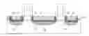
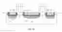
FIG. 1A illustrates a cross-section view of a conventional transistor with an embedded strain-inducing layer. The transistor 100 is formed on a substrate 101 with source and drain regions 103. The substrate 101 may, for instance, be formed from Si. As shown, the strain-inducing layer 105 (e.g., SiGe) is embedded in each of the source and drain regions 103. The geometry of the strain-inducing layer 105 induces a large, uniaxial, strain in the channel region 107, which results in significant improvement in hole mobility. The strain-inducing layer 105 may be deposited by an epitaxial growth process in recesses etched into the source and drain regions 103. However, the growth rate may be different along different surfaces of the recesses. For instance, the thickness of the strain-inducing layer 105 is greatest at the bottom surfaces 109 and then tapers at the edges 111.
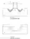
FIG. 1B schematically illustrates a recess 121 formed in the substrate 101. A strain-inducing layer (e.g., SiGe) typically grows at a faster rate at the bottom surface 123 that corresponds to a <100> crystal direction of the substrate 101 than at the sidewall surfaces 125 that correspond to the <110> and <111> directions. As indicated, the <110> and <111> directions may roughly correspond to a surface angle of 54.7 degrees.
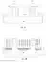
FIGS. 2A through 2E schematically illustrate a process for forming a uniform, embedded strain-inducing layer, according to an exemplary embodiment of the present disclosure.
Adverting to FIG. 2A, recesses 201 are formed in the source and drain regions of the substrate 203 on opposite sides of each gate 205. The U-shaped recesses 201 may be formed after the spacers 207 have been formed. The U-shaped recesses 201 may be formed by a wet or dry etch process. Surfaces of the recesses 201 may correspond to various crystal directions of the underlying substrate 203. For instance, the bottom surfaces (e.g., surface 209) may correspond to a <100> face of a Si substrate and the sidewall surfaces (e.g., surface 211) may correspond to a <110> or <111> face of a Si substrate, though illustrated as perpendicular to the bottom surface.
Adverting to FIG. 2B, the bottom surfaces of the recesses 201 are implanted with a high-dose impurity to form the implanted impurity regions 213. The implanted impurity regions 213 may include, for instance, F, N, Ne, or Ar. A standard metal implantation process may be used. Adverting to FIG. 2C, the sidewall surfaces 215 of the recesses 201 are implanted with a tilted high-dose impurity to form the implanted impurity regions 217. The implanted impurity regions 217 may include, for instance, Ge. A standard metal implant process may be used. The bottom and sidewall surface implants may be performed separately or in a single implantation step. Alternatively, either implanted impurity regions 213 or implanted impurity regions 217 may be used alone (not shown for illustrative convenience). In accordance with this disclosure, “high-dose” is defined as a concentration of the impurity ranging from 1e14 keV to 1e15 keV.
Adverting to FIG. 2D, a strain-inducing layer 219 (e.g., SiGe) is deposited in the recesses 201. Prior to the deposition, a surface cleaning process (e.g., plasma clean and anneal treatment) may be used to clean the surfaces of the doped substrate. The strain-inducing layer 219 may be formed by an epitaxial growth process. As shown, the final shape of the material is more uniform at all points along the recess, particular at the corners (e.g., corner 221) of the recesses 201. For instance, the thickness at the corner and sidewall surfaces of the recesses may be approximately the same as the thickness at the bottom surfaces of the recesses. Adverting to FIG. 2E, a cap 223 (e.g., Si) is formed to fill the recesses.
The final shape of the strain-inducing layer 219 may be adjusted by controlling the concentration of the implanted impurities. The bottom surface implants (e.g., F, N, Ne, or Ar) may downwardly adjust the growth rate whereas the sidewall implants (e.g., Ge) result in a higher growth rate. For instance, the bottom surface implants may retard the growth rate to make it slower than at the sidewall surfaces. By adjusting the relative concentration of the implants to the <100>, <110>, and <111> surfaces, the shape of the resulting strain-inducing layer 219 can be controlled to be more uniform.
The embodiments of the present disclosure can achieve several technical effects, including improved hole mobility and resulting device performance. The present disclosure enjoys industrial applicability in any of various types of highly integrated semiconductor devices used in microprocessors, smart phones, mobile phones, cellular handsets, set-top boxes, DVD recorders and players, automotive navigation, printers and peripherals, networking and telecom equipment, gaming systems, and digital cameras. The present disclosure is particularly applicable to highly integrated 28 nm node and beyond semiconductor devices employing a compressive strain.
In the preceding description, the present disclosure is described with reference to specifically exemplary embodiments thereof. It will, however, be evident that various modifications and changes may be made thereto without departing from the broader spirit and scope of the present disclosure, as set forth in the claims. The specification and drawings are, accordingly, to be regarded as illustrative and not as restrictive. It is understood that the present disclosure is capable of using various other combinations and embodiments and is capable of any changes or modifications within the scope of the inventive concept as expressed herein.
Claims
What is claimed is:1. A method comprising:
forming a recess in a source or drain region of a substrate;
implanting a high-dose impurity in a surface of the recess; and
depositing a silicon-germanium (SiGe) layer in the recess.
2. The method of claim 1, comprising:
implanting the high-dose impurity at a concentration of 1e14 kilo electron volts (keV) to 1e15 keV.
3. The method of claim 2, comprising:
implanting the high-dose impurity along an axis perpendicular to a bottom surface of the recess; or
implanting the high-dose impurity at an angle between 0 and 90 degrees to a side surface of the recess.
4. The method of claim 3, comprising:
implanting fluorine (F), nitrogen (N), neon (Ne), argon (Ar), or a combination thereof, in a bottom surface of the recess; or
implanting germanium (Ge) in a side surface of the recess.
5. The method of claim 3, further comprising:
adjusting a thickness of the SiGe layer based on a concentration of the high-dose impurity.
6. The method of claim 2, comprising:
implanting a first high-dose impurity in a bottom surface of the recess; and
implanting a second high-dose impurity in a sidewall surface of the recess.
7. The method of claim 6, wherein the first high-dose impurity comprises fluorine (F), nitrogen (N), neon (Ne), argon (Ar), or a combination thereof, and the second high-dose impurity comprises germanium (Ge).
8. The method of claim 6, comprising differentially adjusting respective concentrations of the first and second high-dose impurities to obtain a SiGe layer of substantially uniform thickness.
9. The method of claim 1, comprising forming the recess by a dry etch process.
10. A device comprising:
a substrate;
a source or drain region in the substrate;
a recess in the source or drain region;
a high-dose impurity implanted in a surface of the recess; and
a silicon-germanium (SiGe) layer formed in the recess.
11. The device of claim 10, wherein
the high-dose impurity is implanted along an axis perpendicular to a bottom surface of the recess; or
the high-dose impurity is implanted at an angle between 0 and 90 degrees to a side surface of the recess.
12. The method of claim 11 wherein:
the high-dose impurity is implanted in a bottom surface of the recess and comprises fluorine (F), nitrogen (N), neon (Ne), argon (Ar), or a combination thereof
13. The method of claim 11 wherein:
the high-dose impurity is implanted in a side surface of the recess and comprises germanium (Ge).
14. The device of claim 11, wherein a thickness of the SiGe layer is based on a concentration of the high-dose impurity.
15. The device of claim 14, wherein the concentration of the high-dose impurity ranges from 1e14 kilo electron volts (keV) to 1e15 keV.
16. The device of claim 10, comprising a first high-dose impurity implanted in a bottom surface of the recess, and a second high-dose impurity implanted in a sidewall surface of the recess.
17. The device of claim 16, wherein the first high-dose impurity comprises fluorine (F), nitrogen (N), neon (Ne), argon (Ar), or a combination thereof, and the second high-dose impurity comprises germanium (Ge).
18. The device of claim 16, wherein respective concentrations of the first and second high-dose impurities correspond to a SiGe layer of substantially uniform thickness.
19. A method comprising:
forming a recess in a source or drain region of a substrate;
implanting an impurity in a surface of the recess at a concentration of 1e14 kilo electron volts (keV) to 1e15 keV along an axis perpendicular to a bottom surface of the recess or at an angle between 0 and 90 degrees to a side surface of the recess;
epitaxially growing a silicon-germanium (SiGe) layer in the recess; and
adjusting a thickness of the SiGe layer based on the concentration of the impurity.
20. The method of claim 19, further comprising:
implanting a first impurity comprising fluorine (F), nitrogen (N), neon (Ne), argon (Ar), or a combination thereof, to a bottom surface of the recess;
implanting a second impurity comprising germanium (Ge) to a sidewall surface of the recess; and
differentially adjusting respective concentrations of the first and second impurities to obtain a SiGe layer of substantially uniform thickness.
Images & Drawings included:
Sources:
- United States Patent and Trademark Office - verify current appl. status at the USPTO↗
Recent applications in this class:
- » 20250022957 2025-01-16
EPITAXIAL STRUCTURES FOR SEMICONDUCTOR DEVICES AND MANUFACTURING METHODS THEREOF - » 20240429316 2024-12-26
SEMICONDUCTOR DEVICE - » 20240421228 2024-12-19
NOISE TRANSISTOR - » 20240395937 2024-11-28
SEMICONDUCTOR DEVICE HAVING A SHAPED EPITAXIAL REGION WITH SHAPING SECTION - » 20240395936 2024-11-28
SEMICONDUCTOR DEVICE AND MANUFACTURING METHOD THEREOF - » 20240395935 2024-11-28
Structure and Method for FinFET Device with Asymmetric Contact - » 20240363754 2024-10-31
SEMICONDUCTOR DEVICE STRUCTURE WITH CAP LAYER - » 20240363753 2024-10-31
Epitaxial Source/Drain Structure and Method of Forming Same - » 20240363752 2024-10-31
MINIMIZATION OF SILICON GERMANIUM FACETS IN PLANAR METAL OXIDE SEMICONDUCTOR STRUCTURES - » 20240322039 2024-09-26
INTEGRATED CIRCUIT DEVICES
Recent applications for this Assignee:
- » 20220238386 2022-07-28
METHODS, APPARATUS, AND MANUFACTURING SYSTEM FOR SELF-ALIGNED PATTERNING OF A VERTICAL TRANSISTOR - » 20220200636 2022-06-23
Multiband receivers for millimeter wave devices - » 20220085994 2022-03-17
Public-private encryption key generation using Pcell parameter values and on-chip physically unclonable function values - » 20210066503 2021-03-04
Body-contacted field effect transistors configured for test and methods - » 20210063531 2021-03-04
Transmitter unit suitable for millimeter wave devices - » 20210057592 2021-02-25
Semiconductor detectors with butt-end coupled waveguide and method of forming the same - » 20210043727 2021-02-11
Gate-all-around field effect transistors with robust inner spacers and methods - » 20210027005 2021-01-28
Method, apparatus and system for wide metal line for SADP routing - » 20210005601 2021-01-07
Fin-type field effect transistor with reduced fin bulge and method - » 20210005454 2021-01-07
Metal on metal multiple patterning