Redistribution film for IC package
US20160141262A1
2016-05-19
14/542,191
2014-11-14
✅ Patent granted
US 9,756,738 B2
2017-09-05
-
-
Fernando L Toledo | Lawrence-Linh T Nguyen
Jianq Chyun IP Office
2034-11-14
Abstract:
A redistribution film for IC package is disclosed, which comprises a top redistribution layer configured on top of a bottom redistribution layer. The top redistribution layer is fabricated following PCB design rule, and the bottom redistribution layer is fabricated following IC design rule. Further, the interface between the top redistribution layer and the bottom redistribution layer is optionally made roughed to increase bonding forces therebetween.
Applicant:
Interested in similar patents?
Get notified when new applications in this technology area are published.
Classification:
H01L24/17 » CPC main
Arrangements for connecting or disconnecting semiconductor or solid-state bodies; Methods or apparatus related thereto; Means for bonding being attached to, or being formed on, the surface to be connected, e.g. chip-to-package, die-attach, "first-level" interconnects; Manufacturing methods related thereto; Bump connectors ; Manufacturing methods related thereto; Structure, shape, material or disposition of the bump connectors after the connecting process of a plurality of bump connectors
H01L24/11 » CPC further
Arrangements for connecting or disconnecting semiconductor or solid-state bodies; Methods or apparatus related thereto; Means for bonding being attached to, or being formed on, the surface to be connected, e.g. chip-to-package, die-attach, "first-level" interconnects; Manufacturing methods related thereto; Bump connectors ; Manufacturing methods related thereto Manufacturing methods
H01L2224/0231 » CPC further
Indexing scheme for arrangements for connecting or disconnecting semiconductor or solid-state bodies and methods related thereto as covered by; Means for bonding being attached to, or being formed on, the surface to be connected, e.g. chip-to-package, die-attach, "first-level" interconnects; Manufacturing methods related thereto; Bonding areas; Manufacturing methods related thereto; Redistribution layers [RDL] for bonding areas Manufacturing methods of the redistribution layers
H01L2224/02333 » CPC further
Indexing scheme for arrangements for connecting or disconnecting semiconductor or solid-state bodies and methods related thereto as covered by; Means for bonding being attached to, or being formed on, the surface to be connected, e.g. chip-to-package, die-attach, "first-level" interconnects; Manufacturing methods related thereto; Bonding areas; Manufacturing methods related thereto; Redistribution layers [RDL] for bonding areas; Structure of the redistribution layers being a bump
H01L2224/16112 » CPC further
Indexing scheme for arrangements for connecting or disconnecting semiconductor or solid-state bodies and methods related thereto as covered by; Means for bonding being attached to, or being formed on, the surface to be connected, e.g. chip-to-package, die-attach, "first-level" interconnects; Manufacturing methods related thereto; Bump connectors; Manufacturing methods related thereto; Structure, shape, material or disposition of the bump connectors after the connecting process of an individual bump connector; Disposition the bump connector being at least partially embedded in the surface
H01L2224/1703 » CPC further
Indexing scheme for arrangements for connecting or disconnecting semiconductor or solid-state bodies and methods related thereto as covered by; Means for bonding being attached to, or being formed on, the surface to be connected, e.g. chip-to-package, die-attach, "first-level" interconnects; Manufacturing methods related thereto; Bump connectors; Manufacturing methods related thereto; Structure, shape, material or disposition of the bump connectors after the connecting process of a plurality of bump connectors; Structure Bump connectors having different sizes, e.g. different diameters, heights or widths
H01L2224/11334 » CPC further
Indexing scheme for arrangements for connecting or disconnecting semiconductor or solid-state bodies and methods related thereto as covered by; Means for bonding being attached to, or being formed on, the surface to be connected, e.g. chip-to-package, die-attach, "first-level" interconnects; Manufacturing methods related thereto; Bump connectors; Manufacturing methods related thereto; Manufacturing methods by local deposition of the material of the bump connector in solid form using preformed bumps
H01L21/78 » CPC further
Processes or apparatus adapted for the manufacture or treatment of semiconductor or solid state devices or of parts thereof; Manufacture or treatment of devices consisting of a plurality of solid state components formed in or on a common substrate or of parts thereof; Manufacture of integrated circuit devices or of parts thereof; Manufacture or treatment of devices consisting of a plurality of solid state components or integrated circuits formed in, or on, a common substrate with subsequent division of the substrate into plural individual devices
H01L24/81 » CPC further
Arrangements for connecting or disconnecting semiconductor or solid-state bodies; Methods or apparatus related thereto; Methods for connecting semiconductor or other solid state bodies using means for bonding being attached to, or being formed on, the surface to be connected using a bump connector
H01L2924/14 » CPC further
Indexing scheme for arrangements or methods for connecting or disconnecting semiconductor or solid-state bodies as covered by; Details of semiconductor or other solid state devices to be connected; Device type Integrated circuits
H01L23/00 IPC
Details of semiconductor or other solid state devices
H05K3/4682 » CPC main
Apparatus or processes for manufacturing printed circuits; Manufacturing multilayer circuits by building the multilayer layer by layer, i.e. build-up multilayer circuits Manufacture of core-less build-up multilayer circuits on a temporary carrier or on a metal foil
H05K3/4682 » CPC main
Apparatus or processes for manufacturing printed circuits; Manufacturing multilayer circuits by building the multilayer layer by layer, i.e. build-up multilayer circuits Manufacture of core-less build-up multilayer circuits on a temporary carrier or on a metal foil
H01L21/6835 » CPC further
Processes or apparatus adapted for the manufacture or treatment of semiconductor or solid state devices or of parts thereof; Apparatus specially adapted for handling semiconductor or electric solid state devices during manufacture or treatment thereof; Apparatus specially adapted for handling wafers during manufacture or treatment of semiconductor or electric solid state devices or components ; Apparatus not specifically provided for elsewhere for supporting or gripping using temporarily an auxiliary support
H01L24/16 » CPC further
Arrangements for connecting or disconnecting semiconductor or solid-state bodies; Methods or apparatus related thereto; Means for bonding being attached to, or being formed on, the surface to be connected, e.g. chip-to-package, die-attach, "first-level" interconnects; Manufacturing methods related thereto; Bump connectors ; Manufacturing methods related thereto; Structure, shape, material or disposition of the bump connectors after the connecting process of an individual bump connector
H01L24/32 » CPC further
Arrangements for connecting or disconnecting semiconductor or solid-state bodies; Methods or apparatus related thereto; Means for bonding being attached to, or being formed on, the surface to be connected, e.g. chip-to-package, die-attach, "first-level" interconnects; Manufacturing methods related thereto; Layer connectors, e.g. plate connectors, solder or adhesive layers; Manufacturing methods related thereto; Structure, shape, material or disposition of the layer connectors after the connecting process of an individual layer connector
H01L2221/68318 » CPC further
Processes or apparatus adapted for the manufacture or treatment of semiconductor or solid state devices or of parts thereof covered by; Apparatus for handling semiconductor or electric solid state devices during manufacture or treatment thereof; Apparatus for handling wafers during manufacture or treatment of semiconductor or electric solid state devices or components; Apparatus not specifically provided for elsewhere for supporting or gripping using temporarily an auxiliary support Auxiliary support including means facilitating the separation of a device or wafer from the auxiliary support
H01L2221/68359 » CPC further
Processes or apparatus adapted for the manufacture or treatment of semiconductor or solid state devices or of parts thereof covered by; Apparatus for handling semiconductor or electric solid state devices during manufacture or treatment thereof; Apparatus for handling wafers during manufacture or treatment of semiconductor or electric solid state devices or components; Apparatus not specifically provided for elsewhere for supporting or gripping using temporarily an auxiliary support used as a support during manufacture of interconnect decals or build up layers
H01L2224/73204 » CPC further
Indexing scheme for arrangements for connecting or disconnecting semiconductor or solid-state bodies and methods related thereto as covered by; Means for bonding being of different types provided for in two or more of groups; Location after the connecting process on the same surface; Bump and layer connectors the bump connector being embedded into the layer connector
H05K3/46 IPC
Apparatus or processes for manufacturing printed circuits Manufacturing multilayer circuits
H05K3/46 IPC
Apparatus or processes for manufacturing printed circuits Manufacturing multilayer circuits
H01L21/683 IPC
Processes or apparatus adapted for the manufacture or treatment of semiconductor or solid state devices or of parts thereof; Apparatus specially adapted for handling semiconductor or electric solid state devices during manufacture or treatment thereof; Apparatus specially adapted for handling wafers during manufacture or treatment of semiconductor or electric solid state devices or components ; Apparatus not specifically provided for elsewhere for supporting or gripping
H05K2201/10674 » CPC further
Indexing scheme relating to printed circuits covered by; Details of components or other objects attached to or integrated in a printed circuit board; Details of electrical connections of non-printed components, e.g. special leads; Components characterised by their electrical contacts Flip chip
H01L2924/15311 » CPC further
Indexing scheme for arrangements or methods for connecting or disconnecting semiconductor or solid-state bodies as covered by; Details of package parts other than the semiconductor or other solid state devices to be connected; Die mounting substrate; Connection portion the connection portion being formed only on the surface of the substrate opposite to the die mounting surface being a ball array, e.g. BGA
Description
BACKGROUND
1. Technical Field
The present invention relates to a redistribution film for IC package, especially relates to a film composed of double redistribution layers where a top redistribution layer is made and configured on top of a bottom redistribution layer. The top redistribution layer is fabricated following PCB design rule and the bottom redistribution layer is fabricated following IC design rule.
2. Description of Related Art
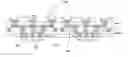
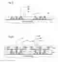
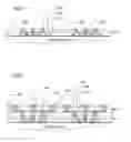
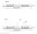
FIG. 1A shows a prior art substrate for IC package
FIG. 1A shows a prior art substrate for IC package disclosed in US2014/0102777A1 which has an embedded silicon interposer 20. The silicon interposer 20 has four lateral sides 206. A molding compound 22 wraps the silicon interposer 20 around the four lateral sides 206. A plurality of via metal 200 is made through the silicon interposer 20. An insulation liner 201 is made between the through via 200 and the silicon interposer 20 for an electrical insulation there-between. A top redistribution layer 21 is made on top of the silicon interposer 20 with a plurality of metal pad 210 exposed on top. The plurality of metal pad 210 on top is provided for accommodating an IC chip (not shown) to mount. A circuit built-up layer 25 is made on bottom of the silicon interposer 20 with a plurality of metal pad 220 configured on bottom. A plurality of solder ball 24 is configured and each solder ball 24 is configured on bottom of a corresponding bottom metal pad 220.
FIG. 1B shows a reversed view of FIG. 1A. FIG. 1B is made to present the prior art of FIG. 1A in a position similar to a package substrate of the present invention to facilitate a comparison there between. FIG. 1B shows an up-down view of FIG. 1A. The top solder ball 24 is configured for mounting the package substrate onto a mother board (not shown). The bottom metal pad 210 is configured for a chip or chips to mount.
BRIEF DESCRIPTION OF THE DRAWINGS
FIGS. 1A˜1B show a prior art substrate for IC package.
FIGS. 2A˜2I show a fabricating process for a first embodiment according to the present invention.
FIGS. 3A˜3I show a fabricating process for a second embodiment according to the present invention.
FIGS. 4A˜4N show a fabricating process for a third embodiment according to the present invention.
DETAILED DESCRIPTION OF THE INVENTION
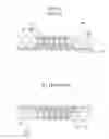
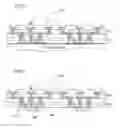
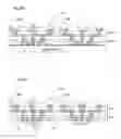
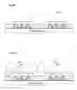
FIGS. 2A˜2I show a fabricating process for a first embodiment according to the present invention.
FIG. 2A shows: preparing a temporary carrier; applying a release layer 31 on top of the temporary carrier; and applying a seed layer 32 on top of the release layer 31.
FIG. 2B shows: applying a patterned photoresist PR on top of the seed layer 32.
FIG. 2C shows: forming a patterned bottom metal pad 341.
FIG. 2D shows: stripping the photoresist 33; and leaving a plurality of bottom metal pad 341.
FIG. 2E shows: forming a bottom redistribution layer RDL1, at least one redistribution circuit 342 is included in the RDL1, the redistribution circuit 342 is made using the bottom metal pad 341 as a start point according to IC design rule or equivalent; forming a plurality of first top metal pad 343 on top of the bottom redistribution layer RDL1. A plurality of dielectric layer 351, 352 is intervened among the circuit 341, 342, 343 according to conventional IC fabricating processes. The circuit 341, 342, 343 are collectively called redistribution circuit.
FIG. 2F shows: forming a top redistribution layer RDL2 according to conventional PCB fabricating processes or equivalent on top of the bottom redistribution layer RDL1; forming a plurality of second top metal pad 443 on top of the top redistribution layer RDL2; at least one redistribution circuit 442 is included and is made using the first top metal pad 343 as a start point. The redistribution 442 is electrically coupled to the second top metal pad 443. The circuit 443, 442 are collectively called redistribution circuit. Dielectric layers 451, 452, 453 are intervened among the redistribution circuit 443, 442. The dielectric material for PCB fabricating process can be one of polyimide (PI), prepreg (PP) or benzocyclobutene (BCB).
FIG. 2G shows: planting a plurality of solder ball 38, each is planted on top of a corresponding second top metal pad 443.
FIG. 2H shows: removing the temporary carrier; and removing the seed layer 32 from bottom of the bottom redistribution layer RDL1; and mounting at least a chip 391 on bottom of the bottom metal pad 341. Underfill 392 is configured in a space between the chip 391 and the metal pad 341.
FIG. 2I shows: a single unit IC package singulated from the product of FIG. 2H.
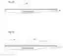
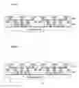
FIG. 3A˜3I fabricating process for a second embodiment according to the present invention.
FIGS. 3A˜3D are the same as FIGS. 2A˜2D, for simplification, the description to FIGS. 3A˜3D is omitted.
FIG. 3E shows: a plurality of recess 382 is made on top of a top dielectric layer of the bottom redistribution layer RDL1. The recess 382 is made to enhance the roughness of the top surface of the bottom redistribution layer RDL1. The increased roughness enhances bonding force to a layer formed on top of the bottom redistribution layer RDL1 in a later fabricating process.
FIGS. 3F˜3I are similar to FIGS. 2F˜2I, we describe again as follows:
FIG. 3F shows: forming a top redistribution layer RDL2 according to conventional PCB fabricating processes or equivalent on top of the bottom redistribution layer RDL1; forming a plurality of second top metal pad 443 on top of the top redistribution layer RDL2; at least one redistribution circuit 442 is included and is made using the first top metal pad 343 as a start point. The redistribution 442 is electrically coupled to the second top metal pad 443. The circuit 443, 442 are collectively called redistribution circuit. Dielectric layers 451, 452, 453 are intervened among the redistribution circuit 443, 442. The dielectric material for PCB fabricating process can be one of polyimide (PI), prepreg (PP) or benzocyclobutene (BCB).
FIG. 3G shows: planting a plurality of solder ball 38, each is planted on top of a corresponding second top metal pad 443.
FIG. 3H shows: removing the temporary carrier; and removing the seed layer 32 from bottom of the bottom redistribution layer RDL1; and mounting at least a chip 391 on bottom of the bottom metal pad 341. Underfill 392 is configured in a space between the chip 391 and the metal pad 341.
FIG. 3I shows: a single unit IC package singulated from the product of FIG. 3H.
FIG. 3I is a single unit of IC package with a roughed interface between top redistribution layer RDL2 and bottom redistribution layer RDL1. The roughness is caused by the plurality of recess 382.
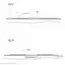
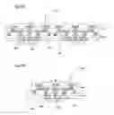
FIG. 4A˜4M fabricating process for a third embodiment according to the present invention.
FIGS. 4A˜4E are the same as FIGS. 2A˜2E, for simplification, the description to FIGS. 4A˜4E is omitted.
FIG. 4F˜4J shows: a plurality of recess 382 is made on a top dielectric layer of the bottom redistribution layer RDL1. The plurality of recess 382 is made to enhance the roughness of the top surface of the bottom redistribution layer RDL1. The increased roughness enhances bonding force to a layer formed on top of the bottom redistribution layer RDL1 in a later fabricating process.
FIG. 4F shows: applying a first patterned photoresist PR1 on top of the bottom redistribution layer RDL1 and exposing partial top surface of the bottom redistribution layer RDL1.
FIG. 4G shows: applying a seed layer 42 on top of the first photoresist PR1 and on the exposed top surface of the bottom redistribution layer RDL1.
FIG. 4H shows: applying a second patterned photoresist PR2 on top of the seed layer 42; forming a plurality of trench 45 to expose the seed layer 42 on a bottom of each corresponding trench 45.
FIG. 4I shows: forming a metal bump 46 in each corresponding trench 45 using the seed layer 42 as a start point.
FIG. 4J shows: stripping the second photoresist PR2; stripping the seed layer 42; stripping the first photoresist PR1; and leaving a plurality of metal bump 46 on top of a top dielectric layer of the bottom redistribution layer RDL1.
FIGS. 4K˜4N are the same as FIGS. 2F˜2I, we describe again as follows:
FIG. 4K shows: forming a top redistribution layer RDL2 according to conventional PCB fabricating processes or equivalent on top of the bottom redistribution layer RDL1; forming a plurality of second top metal pad 443 on top of the top redistribution layer RDL2; at least one redistribution circuit 442 is included and is made using the first top metal pad 343 as a start point. The redistribution 442 is electrically coupled to the second top metal pad 443. The circuit 443, 442 are collectively called redistribution circuit. Dielectric layers 451, 452, 453 are intervened among the redistribution circuit 443, 442. The dielectric material for PCB fabricating process can be one of polyimide (PI), prepreg (PP) or benzocyclobutene (BCB).
FIG. 4L shows: planting a plurality of solder ball 38, each is planted on top of a corresponding second top metal pad 443.
FIG. 4M shows: removing the temporary carrier; and removing the seed layer 32 from bottom of the bottom redistribution layer RDL1; and mounting at least a chip 391 on bottom of the bottom metal pad 341. Underfill 392 is configured in a space between the chip 391 and the metal pad 341.
FIG. 4N shows: a single unit IC package singulated from the product of FIG. 4M.
FIG. 4N is a single unit of IC package with a roughed interface between top redistribution layer RDL2 and bottom redistribution layer RDL1. The roughness is caused by the plurality of metal bump 46.
While several embodiments have been described by way of example, it will be apparent to those skilled in the art that various modifications may be configured without departs from the spirit of the present invention. Such modifications are all within the scope of the present invention, as defined by the appended claims.
Claims
1-5. (canceled)
6. A fabricating process for a redistribution film for IC package, the process comprising:
applying a release layer on top of a temporary carrier;
applying a seed layer on top of the release layer;
applying a first patterned photoresist on top of the seed layer;
forming a plurality of bottom metal pads over the seed layer and in the first patterned photoresist;
stripping the first patterned photoresist;
forming a bottom redistribution layer, layer by layer, according to IC design rule and using the plurality of bottom metal pads as a start point, the bottom redistribution layer including a plurality of first top metal pads exposed on a top surface of the bottom redistribution layer; and
after said forming the bottom redistribution layer, forming a top redistribution layer, layer by layer, according to PCB design rule, directly on top of the bottom redistribution layer and using the plurality of first top metal pads as a start point, the top redistribution layer including a plurality of second top metal pads exposed on a top surface of the top redistribution layer.
7. A fabricating process for a redistribution film for IC package as claimed in claim 6, further comprising:
planting a plurality of solder balls, each configured on a top surface of a corresponding second top metal pad among the plurality of second top metal pads.
8. A fabricating process for a redistribution film for IC package as claimed in claim 7, further comprising:
removing the temporary carrier;
removing the seed layer;
mounting at least one chip on bottom of the bottom metal pads; and
singulating to produce a plurality of IC package units.
9. A fabricating process for a redistribution film for IC package as claimed in claim 6, further comprising:
forming a plurality of recesses on a top surface of a top dielectric layer of the bottom redistribution layer before the top redistribution layer is formed.
10. (canceled)
11. A fabricating process for a redistribution film for IC package as claimed in claim 9, further comprising:
planting a plurality of solder balls, each configured on a top surface of a corresponding second top metal pad among the plurality of second top metal pads.
12. A fabricating process for a redistribution film for IC package as claimed in claim 11, further comprising:
removing the temporary carrier;
removing the seed layer;
mounting at least one chip on bottom of the bottom metal pads; and
singulating to produce a plurality of IC package units.
13. A fabricating process for a redistribution film for IC package as claimed in claim 6, further comprising:
forming a plurality of bumps on top of the bottom redistribution layer before the top redistribution layer is formed.
14. A fabricating process for a redistribution film for IC package as claimed in claim 6, further comprising, before the top redistribution layer is formed:
applying a second patterned photoresist on a top dielectric layer of the bottom redistribution layer while exposing a portion of the top dielectric layer of the bottom redistribution layer;
applying a further seed layer on top of the second patterned photoresist and on the exposed portion of the top dielectric layer of the bottom redistribution layer;
applying a third patterned photoresist on top of the further seed layer, the third patterned photoresist including a plurality of trenches to expose the further seed layer on a bottom of each trench among the plurality of trenches;
forming a plurality of metal bumps, each in a corresponding trench among the plurality of trenches, using the further seed layer as a start point;
stripping the second and third patterned photoresists and the seed layer while leaving the plurality of metal bumps on top of the top dielectric layer of the bottom redistribution layer, wherein the top redistribution layer is formed on top of the plurality of metal bumps and the bottom redistribution layer.
15. A fabricating process for a redistribution film for IC package as claim in claim 14, further comprising:
planting a plurality of solder balls, each configured on a top surface of a corresponding second top metal pad among the plurality of second top metal pads.
16. A fabricating process for a redistribution film for IC package as claim in claim 15, further comprising:
removing the temporary carrier;
removing the seed layer;
mounting at least one chip on bottom of the bottom metal pads; and
singulating to produce a plurality of IC package units.
17-19. (canceled)
20. A redistribution film for IC package, the redistribution film comprising:
a bottom redistribution layer fabricated according to IC design rule, the bottom redistribution layer having a plurality of bottom metal pads and a plurality of first top metal pads, wherein a density of the plurality of bottom metal pads is higher than a density of the plurality of first top metal pads;
a top redistribution layer fabricated according to PCB design rule, the top redistribution layer configured on top of the bottom redistribution layer and having a plurality of second top metal pads, wherein the density of the plurality of first top metal pads is higher than a density of the plurality of second top metal pads;
a plurality of bumps configured on a top surface of the bottom redistribution layer; and
a dielectric layer over the top surface of the bottom redistribution layer,
wherein
the plurality of first top metal pads of the bottom redistribution layer, bottom conductive features of the top redistribution layer, and the plurality of bumps are embedded in the dielectric layer,
the bottom conductive features of the top redistribution layer are in direct electrical and physical contact with the corresponding first top metal pads of the bottom redistribution layer, and
top surfaces of the plurality of bumps are below a top surface of the dielectric layer.
21. A fabricating process for a redistribution film for IC package as claimed in claim 14, further comprising, after said stripping the second and third patterned photoresists and the seed layer:
forming a dielectric layer over the bottom redistribution layer and the plurality of metal bumps,
wherein
the plurality of first top metal pads of the bottom redistribution layer, bottom conductive features of the top redistribution layer, and the plurality of metal bumps are embedded in the dielectric layer,
the bottom conductive features of the top redistribution layer are in direct electrical and physical contact with the corresponding first top metal pads of the bottom redistribution layer, and
top surfaces of the plurality of metal bumps are below a top surface of the dielectric layer.
Images & Drawings included:


Sources:
- United States Patent and Trademark Office - verify current appl. status at the USPTO↗
Similar patent applications:
- » 20170265312
Redistribution film for IC package
Recent applications in this class:
- » 20250149490 2025-05-08
SEMICONDUCTOR PACKAGE - » 20250118694 2025-04-10
HONEYCOMB PATTERN FOR CONDUCTIVE FEATURES - » 20250112193 2025-04-03
SEMICONDUCTOR PACKAGE - » 20250096178 2025-03-20
MICROELECTRONIC PACKAGE WITH SOLDER ARRAY THERMAL INTERFACE MATERIAL (SA-TIM) - » 20250079379 2025-03-06
SEMICONDUCTOR DEVICE - » 20250006685 2025-01-02
SEMICONDUCTOR PACKAGES WITH MULTIPLE TYPES OF CONDUCTIVE COMPONENTS - » 20240421113 2024-12-19
UNIFORM CHIP GAPS VIA INJECTION-MOLDED SOLDER PILLARS - » 20240421112 2024-12-19
SEMICONDUCTOR ELEMENT AND SEMICONDUCTOR DEVICE - » 20240395755 2024-11-28
SEMICONDUCTOR PACKAGE - » 20240304583 2024-09-12
SEMICONDUCTOR DEVICE AND MANUFACTURING METHOD THEREOF