Method of making an electronic device including two-step encapsulation and related devices
US20160190029A1
2016-06-30
14/585,566
2014-12-30
✅ Patent granted
US 9,379,034 B1
2016-06-28
-
-
Dung Le
Allen, Dyer, Doppelt, Milbrath & Gilchrist, P.A.
2034-12-30
Abstract:
A method of making an electronic device may include positioning an integrated circuit (IC) die on an upper surface of a grid array substrate having connections on a lower surface thereof and coupling respective bond pads of the IC die to the grid array with bond wires. The method may also include forming a first encapsulating layer over the IC die and bond wires and positioning a heat spreader on the substrate above the first encapsulating layer after forming the first encapsulating layer. The method may further include forming a second encapsulating layer over the first encapsulating layer and embedding the heat spreader in the second encapsulating layer.
Inventors:
- Yiyi Ma 11 🇸🇬 Singapore, Singapore
- Xueren Zhang 18 🇸🇬 Singapore, Singapore
- Kim-Yong Goh 30 🇸🇬 Singapore, Singapore
Assignee:
- STMICROELECTRONICS PTE LTD. 284 🇸🇬 Singapore, Singapore
Applicant:
Interested in similar patents?
Get notified when new applications in this technology area are published.
Classification:
H01L23/49816 » CPC further
Details of semiconductor or other solid state devices; Arrangements for conducting electric current to or from the solid state body in operation, e.g. leads, terminal arrangements ; Selection of materials therefor consisting of soldered constructions; Leads, on insulating substrates,; Additional leads joined to the metallisation on the insulating substrate, e.g. pins, bumps, wires, flat leads Spherical bumps on the substrate for external connection, e.g. ball grid arrays [BGA]
H01L24/85 » CPC further
Arrangements for connecting or disconnecting semiconductor or solid-state bodies; Methods or apparatus related thereto; Methods for connecting semiconductor or other solid state bodies using means for bonding being attached to, or being formed on, the surface to be connected using a wire connector
H01L2924/14 » CPC further
Indexing scheme for arrangements or methods for connecting or disconnecting semiconductor or solid-state bodies as covered by; Details of semiconductor or other solid state devices to be connected; Device type Integrated circuits
H01L23/31 IPC
Details of semiconductor or other solid state devices; Encapsulations, e.g. encapsulating layers, coatings, e.g. for protection characterised by the arrangement or shape
H01L23/498 IPC
Details of semiconductor or other solid state devices; Arrangements for conducting electric current to or from the solid state body in operation, e.g. leads, terminal arrangements ; Selection of materials therefor consisting of soldered constructions Leads, on insulating substrates,
H01L23/367 IPC
Details of semiconductor or other solid state devices; Arrangements for cooling, heating, ventilating or temperature compensation ; Temperature sensing arrangements; Selection of materials, or shaping, to facilitate cooling or heating, e.g. heatsinks Cooling facilitated by shape of device
H01L23/00 IPC
Details of semiconductor or other solid state devices
H01L23/3675 » CPC further
Details of semiconductor or other solid state devices; Arrangements for cooling, heating, ventilating or temperature compensation ; Temperature sensing arrangements; Selection of materials, or shaping, to facilitate cooling or heating, e.g. heatsinks; Cooling facilitated by shape of device characterised by the shape of the housing
H01L23/3135 » CPC main
Details of semiconductor or other solid state devices; Encapsulations, e.g. encapsulating layers, coatings, e.g. for protection characterised by the arrangement or shape the device being completely enclosed Double encapsulation or coating and encapsulation
H01L24/49 » CPC further
Arrangements for connecting or disconnecting semiconductor or solid-state bodies; Methods or apparatus related thereto; Means for bonding being attached to, or being formed on, the surface to be connected, e.g. chip-to-package, die-attach, "first-level" interconnects; Manufacturing methods related thereto; Wire connectors; Manufacturing methods related thereto; Structure, shape, material or disposition of the wire connectors after the connecting process of a plurality of wire connectors
H01L23/10 IPC
Details of semiconductor or other solid state devices; Containers; Seals characterised by the material or arrangement of seals between parts, e.g. between cap and base of the container or between leads and walls of the container
H01L21/56 » CPC further
Processes or apparatus adapted for the manufacture or treatment of semiconductor or solid state devices or of parts thereof; Manufacture or treatment of semiconductor devices or of parts thereof the devices having at least one potential-jump barrier or surface barrier, e.g. PN junction, depletion layer or carrier concentration layer; Assembly of semiconductor devices using processes or apparatus not provided for in a single one of the subgroups - , e.g. sealing of a cap to a base of a container Encapsulations, e.g. encapsulation layers, coatings
Description
TECHNICAL FIELD
The present invention is directed to electronic devices, and more particularly, to method of making an electronic device including an integrated circuit and related devices.
BACKGROUND
As electronic devices become relatively smaller, packaging may become of particular interest. For example, a low-k interlayer dielectric (ILD) material may be used in place of a SiO2 ILD to reduce interconnect delay, for example.
The introduction of a low-K ILD material into silicon may impose new challenges for high wire density packaging. In particular, the inherently weak adhesion in the low-k interconnect makes the silicon more susceptible to a failure that may often be called ILD crack or delamination. ILD crack or delamination causes failure of the electronic device, which often happens during temperature cycling tests, for example. The technical article entitled, “Packaging Challenges in Low-k Silicon with Thermally Enhanced Ball Grid Array (TE-PBGA)”, EPTC 2010 by Tran et al. highlights the problems with a low-K ILD material.
As described in the Tran et al. technical article, one cause of the low-k failure has been determined to be the non-uniform distribution of mold compound fillers in the die corner opposite the mold gate. The drop-in heat spreader obstructs the mold compound flow during the transfer molding process, which resulted in greater filler loss in this corner.
SUMMARY
A method of making an electronic device may include positioning an integrated circuit (IC) die on an upper surface of a grid array substrate having a plurality of connections on a lower surface thereof and coupling respective bond pads of the IC die to the grid array with bond wires. The method may also include forming a first encapsulating layer over the IC die and bond wires and positioning a heat spreader on the substrate above the first encapsulating layer after forming the first encapsulating layer. The method may further include forming a second encapsulating layer over the first encapsulating layer and embedding the heat spreader in the second encapsulating layer. Accordingly, the method may decrease failure of the electronic device, for example with a two-step encapsulation which may reduce ILD crack and delamination.
The IC die may be rectangularly shaped, for example. Forming the first encapsulating layer may include forming the first encapsulating layer to extend over and cover each corner of the rectangularly shaped IC die.
The first and second encapsulating layers may each include a same encapsulation material. In other embodiments, the first and second encapsulating layers may each include a different encapsulation material. The IC die may include a low-k interlayer dielectric.
Forming the first encapsulating layer may include positioning a first mold onto the grid array substrate, filling the first mold with a first encapsulation material, curing the first encapsulation material, and removing the first mold, for example. Forming the second encapsulating layer may include positioning a second mold onto the grid array substrate, filling the second mold with a second encapsulation material, curing the second encapsulation material, and removing the second mold. Forming the first encapsulating layer may include applying a body of encapsulation material over the IC, and curing the body of encapsulation material, for example.
A device aspect is directed to an electronic device that may include a grid array substrate having a plurality of connections on a lower surface thereof and an integrated circuit (IC) die on an upper surface of the grid array substrate and having bond pads. The electronic device may also include a plurality of bond wires respectively coupling the bond pads to the grid array, a first encapsulating layer having a first encapsulating material over the IC die and bond wires, and a heat spreader carried by the grid array substrate above and spaced from the first encapsulating layer after. The electronic device may further include a second encapsulating layer having a second encapsulating material different than the first encapsulating material over the first encapsulating layer and embedding the heat spreader in the second encapsulating layer.
BRIEF DESCRIPTION OF THE DRAWINGS
FIGS. 1a-1i are schematic cross-sectional views of an electronic device as it is made according to a method of making an electronic device according to an embodiment.
FIGS. 2a-2g are schematic cross-sectional views of an electronic device as it is make according to a method of making an electronic device according to another embodiment.
FIG. 3 is a perspective cut-away view of an electronic device in accordance with an embodiment.
DETAILED DESCRIPTION
The present invention will now be described more fully hereinafter with reference to the accompanying drawings, in which preferred embodiments of the invention are shown. This invention may, however, be embodied in many different forms and should not be construed as limited to the embodiments set forth herein. Rather, these embodiments are provided so that this disclosure will be thorough and complete, and will fully convey the scope of the invention to those skilled in the art. Like numbers refer to like elements throughout, and prime notation is used to indicate similar elements in alternative embodiments.
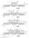
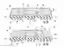
Referring initially to FIGS. 1a-1i, a method of making an electronic device 20 is described. The method includes positioning an integrated circuit (IC) die 21 on an upper surface 23 of a grid array substrate 22. The IC die 21 may include a low-k interlayer dielectric 28 and illustratively has a rectangular shape (FIG. 1a). Of course, the IC die 21 may have other and/or additional interlayers of a same or different material, and may also have a different shape.
The grid array substrate 22 has connections 25 on a lower surface 24 thereof. The grid array substrate 22 is illustratively a ball grid array (BGA) substrate, and more particularly, a plastic ball grid array substrate (PBGA). Of course, the grid array substrate 22 may be another type of substrate, as will be appreciated by those skilled in the art.
The method includes coupling respective bond pads 26 of the IC die 21 to the grid array substrate 22 with bond wires 27 (FIG. 1b). The method also includes include forming a first encapsulating layer 30 over the IC die 21 and bond wires 27. The first encapsulating layer 30 is formed to extend over and cover each corner of the rectangularly shaped IC die 21.
To form the first encapsulating layer 30 a first mold 31 is positioned onto the grid array substrate 22 (FIG. 1c). The first mold 31 is filled with a first encapsulation material 32 and cured (FIG. 1d). The first mold 31 is then removed (FIG. 1e). The first encapsulation material 32 illustratively does not extend to ends of the grid array substrate 22.
The method further includes positioning a heat spreader 51 on the grid array substrate 22 above and spaced from the first encapsulating layer 30 after forming the first encapsulating layer (FIG. 1f). The heat spreader 51 may be copper for example, and is illustratively positioned so that is exposed on an upper surface of the electronic device 20.
After positioning the heat spreader 51, the method further includes forming a second encapsulating layer 40 over the first encapsulating layer 30 and embedding the heat spreader 51 in the second encapsulating layer. The second encapsulating layer 40 is formed by positioning a second mold 41 onto the grid array substrate 22 (FIG. 1g), filling the second mold with a second encapsulation material 42 and curing the second encapsulation material (FIG. 1h), and removing the second mold (FIG. 1i). The first and second encapsulation materials may each be the same material. In some embodiments, the first and second encapsulation materials may be different materials.
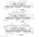
Referring now to FIGS. 2a-2g, in another embodiment, the first encapsulating layer 30′ is formed by applying a body of first encapsulation material 55′ over the IC die 21′. The body of first encapsulation material 55′ (FIG. 2c) is a glob top material, for example. More particularly, the body of first encapsulation material 55′ may be a low modulus glob top resin that may be a thermosetting or a thermoplastic resin. In other words, no mold is used. As will be appreciated by those skilled in the art, a low modulus glob top resin, for example, may advantageously provide a relatively low cost packaging approach for chip-on-board technology.
It should be noted that while not specifically described, the method steps corresponding to FIGS. 2a-2b are similar to those described with respect to FIGS. 1a-1b. The body of first encapsulation material 55′ is allowed to cure.
Similar to the embodiment described above, and particularly, with respect to FIG. 1f, the method of the present embodiment further includes positioning a heat spreader 51′ on the grid array substrate 22′ above and spaced from the first encapsulating layer 30′ after forming the first encapsulating layer (FIG. 2d).
After positioning the heat spreader 51′, the method further includes forming a second encapsulating layer 40′ over the first encapsulating layer 30′ and embedding the heat spreader 51′ in the second encapsulating layer. The second encapsulating layer 40′ is formed by positioning a second mold 41′ onto the grid array substrate 22′ (FIG. 2e), filling the second mold with a second encapsulation material and curing the second encapsulation material (FIG. 2f), and removing the second mold (FIG. 2g). Of course, in some embodiments, the second mold and second encapsulation material may be replaced with a second body of encapsulating material, for example a glob top material.
Indeed, as will be appreciated by those skilled in the art, the forming of the first and second encapsulation layers advantageously may provide a more uniform distribution of the encapsulating material in the corners of the die opposite a gate of the mold gate. In prior art encapsulating methods, the heat spreader generally obstructed the flow of the encapsulating material during the transfer molding process, which resulted in greater loss of encapsulating material in this corner. The two-step method of forming the first and second encapsulating layers may provide reduced losses in the corners of the die, and may thus reduce failure.
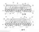
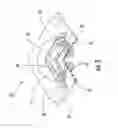
Referring now additionally to FIG. 3, a device aspect is directed to an electronic device 20 that includes a grid array substrate 22 having a plurality of connections 25 on a lower surface 24 thereof and an IC die 21 on an upper surface 23 and having bond pads 26. The electronic device 20 also includes a plurality of bond wires 27 respectively coupling the bond pads 26 to the grid array substrate 22, and a first encapsulating layer 30 having a first encapsulating material over the IC die 21 and bond wires 27. A heat spreader 51 is carried by the grid array substrate 22 above and spaced from the first encapsulating layer 30. A second encapsulating layer 40 having a second encapsulating material different than the first encapsulating material is over the first encapsulating layer 30 and embeds the heat spreader 51 in the second encapsulating layer.
Many modifications and other embodiments of the invention will come to the mind of one skilled in the art having the benefit of the teachings presented in the foregoing descriptions and the associated drawings. Therefore, it is understood that the invention is not to be limited to the specific embodiments disclosed, and that modifications and embodiments are intended to be included within the scope of the appended claims.
Claims
1. A method of making an electronic device comprising:
positioning an integrated circuit (IC) die on an upper surface of a grid array substrate having a plurality of connections on a lower surface thereof;
coupling respective bond pads of the IC die to the grid array substrate with bond wires;
forming a first encapsulating layer over the IC die and bond wires;
positioning a heat spreader on the substrate above the first encapsulating layer after forming the first encapsulating layer, the heat spreader comprising at least one leg coupled to and extending upwardly from the substrate and a body coupled to the at least one leg and spaced above the first encapsulating layer; and
forming a second encapsulating layer over the first encapsulating layer and embedding the heat spreader in the second encapsulating layer.
2. The method of claim 1 wherein the IC die is rectangularly shaped, and wherein forming the first encapsulating layer comprises forming the first encapsulating layer to extend over and cover each corner of the rectangularly shaped IC die.
3. The method of claim 1 wherein the first and second encapsulating layers each comprises a same encapsulating material.
4. The method of claim 1 wherein the first and second encapsulating layers each comprises a different encapsulating material.
5. The method of claim 1 wherein the IC die comprises a low-k interlayer dielectric.
6. The method of claim 1 wherein forming the first encapsulating layer comprises positioning a first mold onto the grid array substrate, filling the first mold with a first encapsulation material, curing the first encapsulation material, and removing the first mold.
7. The method of claim 1 wherein forming the second encapsulating layer comprises positioning a second mold onto the grid array substrate, filling the second mold with a second encapsulation material, curing the second encapsulation material, and removing the second mold.
8. The method of claim 1 wherein forming the first encapsulating layer comprises applying a body of encapsulation material over the IC, and curing the body of encapsulation material.
9. A method of making an electronic device comprising:
positioning an integrated circuit (IC) die on an upper surface of a grid array substrate having a plurality of connections on a lower surface thereof;
coupling respective bond pads of the IC die to the grid array substrate with bond wires;
forming a first encapsulating layer over the IC die and bond wires by
positioning a first mold onto the grid array substrate,
filling the first mold with a first encapsulation material,
curing the first encapsulation material, and
removing the first mold;
positioning a heat spreader on the substrate above the first encapsulating layer after forming the first encapsulating layer; and
forming a second encapsulating layer over the first encapsulating layer and embedding the heat spreader in the second encapsulating layer by
positioning a second mold onto the grid array substrate,
filling the second mold with a second encapsulating material,
curing the second encapsulation material, and
removing the second mold.
10. The method of claim 9 wherein the IC die is rectangularly shaped, and wherein forming the first encapsulating layer comprises forming the first encapsulating layer to extend over and cover each corner of the rectangularly shaped IC die.
11. The method of claim 9 wherein the first and second encapsulating layers each comprises a same encapsulation material.
12. The method of claim 9 wherein the first and second encapsulating layers each comprises a different encapsulation material.
13. The method of claim 9 wherein the IC die comprises a low-k interlayer dielectric.
14. The method of claim 9 wherein forming the first encapsulating layer over the IC comprises applying a body of encapsulation material over the IC, and curing the body of encapsulation material.
15. An electronic device comprising:
a grid array substrate having a plurality of connections on a lower surface thereof;
an integrated circuit (IC) die on an upper surface of said grid array substrate and having bond pads;
a plurality of bond wires respectively coupling said bond pads to said grid array substrate;
a first encapsulating layer having a first encapsulating material over the IC die and bond wires;
a heat spreader carried by said grid array substrate above and spaced from said first encapsulating layer, said heat spreader comprising at least one leg coupled to and extending upwardly from said grid array substrate and a body coupled to the at least one leg and spaced above said first encapsulating layer; and
a second encapsulating layer having a second encapsulating material different than the first encapsulating material over the first encapsulating layer and embedding the heat spreader in the second encapsulating layer.
16. The electronic device of claim 15 wherein the IC die is rectangularly shaped, and wherein the first encapsulating layer extends over and covers each corner of the rectangularly shaped IC die.
17. The electronic device of claim 15 wherein the IC die comprises a low-k interlayer dielectric.
18. A method of making an electronic device comprising:
positioning an integrated circuit (IC) die on an upper surface of a grid array substrate having a plurality of connections on a lower surface thereof;
coupling respective bond pads of the IC die to the grid array substrate with bond wires;
forming a first encapsulating layer over the IC die and bond wires;
positioning a heat spreader on the substrate above the first encapsulating layer after forming the first encapsulating layer; and
forming a second encapsulating layer over the first encapsulating layer and embedding the heat spreader in the second encapsulating layer;
the first and second encapsulating layers each comprising a same encapsulating material.
19. The method of claim 18 wherein the IC die is rectangularly shaped, and wherein forming the first encapsulating layer comprises forming the first encapsulating layer to extend over and cover each corner of the rectangularly shaped IC die.
20. The method of claim 18 wherein the IC die comprises a low-k interlayer dielectric.
21. The method of claim 18 wherein forming the first encapsulating layer comprises applying a body of encapsulation material over the IC, and curing the body of encapsulation material.
Images & Drawings included:


Sources:
- United States Patent and Trademark Office - verify current appl. status at the USPTO↗
Recent applications in this class:
- » 20250293108 2025-09-18
SEMICONDUCTOR PACKAGE AND MANUFACTURING METHOD FOR THE SAME - » 20250285928 2025-09-11
SEMICONDUCTOR PACKAGE AND METHOD OF MANUFACTURING THE SAME - » 20250246493 2025-07-31
SEMICONDUCTOR DEVICE - » 20250239499 2025-07-24
ULTRA-THIN PACKAGED COMPONENT - » 20250233036 2025-07-17
INTEGRATED CIRCUIT WITH A PROTECTIVE LAYER - » 20250226276 2025-07-10
SEMICONDUCTOR DEVICE - » 20250210434 2025-06-26
SEMICONDUCTOR PACKAGE - » 20250210433 2025-06-26
PACKAGE STRUCTURE - » 20250167060 2025-05-22
THREE-DIMENSIONAL INTEGRATED CIRCUIT STRUCTURES AND METHODS OF FORMING THE SAME - » 20250140625 2025-05-01
SEMICONDUCTOR MODULE AND METHOD OF MANUFACTURING A SEMICONDUCTOR MODULE
Recent applications for this Assignee:
- » 20250293190 2025-09-18
WAFER LEVEL CHIP SCALE PACKAGE HAVING VARYING THICKNESSES - » 20250192111 2025-06-12
STACKED DIE PACKAGE INCLUDING A MULTI-CONTACT INTERCONNECT - » 20250174616 2025-05-29
LOW PROFILE SENSOR PACKAGES - » 20250171294 2025-05-29
MEMS THIN MEMBRANE WITH STRESS STRUCTURE - » 20250079189 2025-03-06
OPTICAL SENSOR PACKAGE AND METHOD OF MAKING AN OPTICAL SENSOR PACKAGE - » 20240404905 2024-12-05
PASSIVATION LAYER FOR AN INTEGRATED CIRCUIT DEVICE THAT PROVIDES A MOISTURE AND PROTON BARRIER - » 20240379741 2024-11-14
POWER MOSFET WITH REDUCED CURRENT LEAKAGE AND METHOD OF FABRICATING THE POWER MOSFET - » 20240282881 2024-08-22
EMBEDDED WAFER LEVEL OPTICAL SENSOR PACKAGING - » 20240194709 2024-06-13
SLANTED GLASS EDGE FOR IMAGE SENSOR PACKAGE - » 20240145258 2024-05-02
PANEL LEVEL SEMICONDUCTOR PACKAGE AND METHOD OF MANUFACTURING THE SAME