Chip on chip attach (passive IPD and PMIC) flip chip BGA using new cavity BGA substrate
US20170040309A1
2017-02-09
15/299,910
2016-10-21
✅ Patent granted
US 9,929,130 B2
2018-03-27
-
-
Chuong A Luu
Saile Ackerman LLC | Stephen B. Ackerman | Rosemary L.S. Pike
2036-10-21
Abstract:
An integrated passive device and power management integrated circuit are directly connected, active surface to active surface, resulting in a pyramid die stack. The die stack is flip-chip attached to a laminate substrate having a cavity drilled therein wherein the smaller die fits into the cavity. The die to die attach is not limited to IPD and PMIC and can be used for other die types as required.
Assignee:
- DIALOG SEMICONDUCTOR GMBH 271 🇩🇪 Kirchheim/Teck-Nabern, Germany
Applicant:
Interested in similar patents?
Get notified when new applications in this technology area are published.
Classification:
H01L23/3128 » CPC further
Details of semiconductor or other solid state devices; Encapsulations, e.g. encapsulating layers, coatings, e.g. for protection characterised by the arrangement or shape the device being completely enclosed a substrate forming part of the encapsulation the substrate having spherical bumps for external connection
H01L25/50 » CPC main
Assemblies consisting of a plurality of individual semiconductor or other solid state devices ; Multistep manufacturing processes thereof Multistep manufacturing processes of assemblies consisting of devices, each device being of a type provided for in group or
H01L21/563 » CPC further
Processes or apparatus adapted for the manufacture or treatment of semiconductor or solid state devices or of parts thereof; Manufacture or treatment of semiconductor devices or of parts thereof the devices having at least one potential-jump barrier or surface barrier, e.g. PN junction, depletion layer or carrier concentration layer; Assembly of semiconductor devices using processes or apparatus not provided for in a single one of the subgroups - , e.g. sealing of a cap to a base of a container; Encapsulations, e.g. encapsulation layers, coatings Encapsulation of active face of flip-chip device, e.g. underfilling or underencapsulation of flip-chip, encapsulation preform on chip or mounting substrate
H01L21/565 » CPC further
Processes or apparatus adapted for the manufacture or treatment of semiconductor or solid state devices or of parts thereof; Manufacture or treatment of semiconductor devices or of parts thereof the devices having at least one potential-jump barrier or surface barrier, e.g. PN junction, depletion layer or carrier concentration layer; Assembly of semiconductor devices using processes or apparatus not provided for in a single one of the subgroups - , e.g. sealing of a cap to a base of a container; Encapsulations, e.g. encapsulation layers, coatings Moulds
H01L23/293 » CPC further
Details of semiconductor or other solid state devices; Encapsulations, e.g. encapsulating layers, coatings, e.g. for protection characterised by the material, e.g. carbon Organic, e.g. plastic
H01L23/49816 » CPC further
Details of semiconductor or other solid state devices; Arrangements for conducting electric current to or from the solid state body in operation, e.g. leads, terminal arrangements ; Selection of materials therefor consisting of soldered constructions; Leads, on insulating substrates,; Additional leads joined to the metallisation on the insulating substrate, e.g. pins, bumps, wires, flat leads Spherical bumps on the substrate for external connection, e.g. ball grid arrays [BGA]
H01L23/49866 » CPC further
Details of semiconductor or other solid state devices; Arrangements for conducting electric current to or from the solid state body in operation, e.g. leads, terminal arrangements ; Selection of materials therefor consisting of soldered constructions; Leads, on insulating substrates, characterised by the materials
H01L23/49894 » CPC further
Details of semiconductor or other solid state devices; Arrangements for conducting electric current to or from the solid state body in operation, e.g. leads, terminal arrangements ; Selection of materials therefor consisting of soldered constructions; Leads, on insulating substrates, characterised by the materials Materials of the insulating layers or coatings
H01L24/81 » CPC further
Arrangements for connecting or disconnecting semiconductor or solid-state bodies; Methods or apparatus related thereto; Methods for connecting semiconductor or other solid state bodies using means for bonding being attached to, or being formed on, the surface to be connected using a bump connector
H01L25/0657 » CPC further
Assemblies consisting of a plurality of individual semiconductor or other solid state devices ; Multistep manufacturing processes thereof all the devices being of a type provided for in the same subgroup of groups - , e.g. assemblies of rectifier diodes the devices not having separate containers the devices being of a type provided for in group Stacked arrangements of devices
H01L23/29 IPC
Details of semiconductor or other solid state devices; Encapsulations, e.g. encapsulating layers, coatings, e.g. for protection characterised by the material, e.g. carbon
H01L2225/06517 » CPC further
Details relating to assemblies covered by the group but not provided for in its subgroups; All the devices being of a type provided for in the same subgroup of groups - the devices not having separate containers the devices being of a type provided for in group; Stacked arrangements of devices Bump or bump-like direct electrical connections from device to substrate
H01L2225/06568 » CPC further
Details relating to assemblies covered by the group but not provided for in its subgroups; All the devices being of a type provided for in the same subgroup of groups - the devices not having separate containers the devices being of a type provided for in group; Stacked arrangements of devices; Geometry of the stack, e.g. form of the devices, geometry to facilitate stacking the devices decreasing in size, e.g. pyramidical stack
H01L2924/15311 » CPC further
Indexing scheme for arrangements or methods for connecting or disconnecting semiconductor or solid-state bodies as covered by; Details of package parts other than the semiconductor or other solid state devices to be connected; Die mounting substrate; Connection portion the connection portion being formed only on the surface of the substrate opposite to the die mounting surface being a ball array, e.g. BGA
H01L2924/15313 » CPC further
Indexing scheme for arrangements or methods for connecting or disconnecting semiconductor or solid-state bodies as covered by; Details of package parts other than the semiconductor or other solid state devices to be connected; Die mounting substrate; Connection portion the connection portion being formed only on the surface of the substrate opposite to the die mounting surface being a land array, e.g. LGA
H01L2924/18161 » CPC further
Indexing scheme for arrangements or methods for connecting or disconnecting semiconductor or solid-state bodies as covered by; Details of package parts other than the semiconductor or other solid state devices to be connected; Encapsulation; Shape; Exposing the passive side of the semiconductor or solid-state body of a flip chip
H01L2924/19041 » CPC further
Indexing scheme for arrangements or methods for connecting or disconnecting semiconductor or solid-state bodies as covered by; Details of hybrid assemblies other than the semiconductor or other solid state devices to be connected; Structure; Component type being a capacitor
H01L2924/19042 » CPC further
Indexing scheme for arrangements or methods for connecting or disconnecting semiconductor or solid-state bodies as covered by; Details of hybrid assemblies other than the semiconductor or other solid state devices to be connected; Structure; Component type being an inductor
H01L2924/19043 » CPC further
Indexing scheme for arrangements or methods for connecting or disconnecting semiconductor or solid-state bodies as covered by; Details of hybrid assemblies other than the semiconductor or other solid state devices to be connected; Structure; Component type being a resistor
H01L2924/19051 » CPC further
Indexing scheme for arrangements or methods for connecting or disconnecting semiconductor or solid-state bodies as covered by; Details of hybrid assemblies other than the semiconductor or other solid state devices to be connected; Shape Impedance matching structure [e.g. balun]
H01L2924/19104 » CPC further
Indexing scheme for arrangements or methods for connecting or disconnecting semiconductor or solid-state bodies as covered by; Details of hybrid assemblies other than the semiconductor or other solid state devices to be connected; Disposition of discrete passive components in a stacked assembly with the semiconductor or solid state device on the semiconductor or solid-state device, i.e. passive-on-chip
H01L21/56 IPC
Processes or apparatus adapted for the manufacture or treatment of semiconductor or solid state devices or of parts thereof; Manufacture or treatment of semiconductor devices or of parts thereof the devices having at least one potential-jump barrier or surface barrier, e.g. PN junction, depletion layer or carrier concentration layer; Assembly of semiconductor devices using processes or apparatus not provided for in a single one of the subgroups - , e.g. sealing of a cap to a base of a container Encapsulations, e.g. encapsulation layers, coatings
H01L25/00 IPC
Assemblies consisting of a plurality of individual semiconductor or other solid state devices ; Multistep manufacturing processes thereof
H01L23/00 IPC
Details of semiconductor or other solid state devices
H01L23/31 IPC
Details of semiconductor or other solid state devices; Encapsulations, e.g. encapsulating layers, coatings, e.g. for protection characterised by the arrangement or shape
H01L25/065 IPC
Assemblies consisting of a plurality of individual semiconductor or other solid state devices ; Multistep manufacturing processes thereof all the devices being of a type provided for in the same subgroup of groups - , e.g. assemblies of rectifier diodes the devices not having separate containers the devices being of a type provided for in group
H01L25/16 » CPC further
Assemblies consisting of a plurality of individual semiconductor or other solid state devices ; Multistep manufacturing processes thereof the devices being of types provided for in two or more different main groups of - , e.g. forming hybrid circuits
H01L2225/06513 » CPC further
Details relating to assemblies covered by the group but not provided for in its subgroups; All the devices being of a type provided for in the same subgroup of groups - the devices not having separate containers the devices being of a type provided for in group; Stacked arrangements of devices Bump or bump-like direct electrical connections between devices, e.g. flip-chip connection, solder bumps
H01L23/498 IPC
Details of semiconductor or other solid state devices; Arrangements for conducting electric current to or from the solid state body in operation, e.g. leads, terminal arrangements ; Selection of materials therefor consisting of soldered constructions Leads, on insulating substrates,
H01L24/13 » CPC further
Arrangements for connecting or disconnecting semiconductor or solid-state bodies; Methods or apparatus related thereto; Means for bonding being attached to, or being formed on, the surface to be connected, e.g. chip-to-package, die-attach, "first-level" interconnects; Manufacturing methods related thereto; Bump connectors ; Manufacturing methods related thereto; Structure, shape, material or disposition of the bump connectors prior to the connecting process of an individual bump connector
H01L24/32 » CPC further
Arrangements for connecting or disconnecting semiconductor or solid-state bodies; Methods or apparatus related thereto; Means for bonding being attached to, or being formed on, the surface to be connected, e.g. chip-to-package, die-attach, "first-level" interconnects; Manufacturing methods related thereto; Layer connectors, e.g. plate connectors, solder or adhesive layers; Manufacturing methods related thereto; Structure, shape, material or disposition of the layer connectors after the connecting process of an individual layer connector
H01L23/13 » CPC further
Details of semiconductor or other solid state devices; Mountings, e.g. non-detachable insulating substrates characterised by the shape
H01L2224/73204 » CPC further
Indexing scheme for arrangements for connecting or disconnecting semiconductor or solid-state bodies and methods related thereto as covered by; Means for bonding being of different types provided for in two or more of groups; Location after the connecting process on the same surface; Bump and layer connectors the bump connector being embedded into the layer connector
H01L2924/12042 » CPC further
Indexing scheme for arrangements or methods for connecting or disconnecting semiconductor or solid-state bodies as covered by; Details of semiconductor or other solid state devices to be connected; Device type; Passive devices, e.g. 2 terminal devices; Optical Diode LASER
H01L2924/15156 » CPC further
Indexing scheme for arrangements or methods for connecting or disconnecting semiconductor or solid-state bodies as covered by; Details of package parts other than the semiconductor or other solid state devices to be connected; Die mounting substrate; Shape the die mounting substrate comprising a recess for hosting the device the shape of the recess being other than a cuboid Side view
H01L2924/181 » CPC further
Indexing scheme for arrangements or methods for connecting or disconnecting semiconductor or solid-state bodies as covered by; Details of package parts other than the semiconductor or other solid state devices to be connected Encapsulation
H01L2924/19011 » CPC further
Indexing scheme for arrangements or methods for connecting or disconnecting semiconductor or solid-state bodies as covered by; Details of hybrid assemblies other than the semiconductor or other solid state devices to be connected; Structure including integrated passive components
H01L24/16 » CPC further
Arrangements for connecting or disconnecting semiconductor or solid-state bodies; Methods or apparatus related thereto; Means for bonding being attached to, or being formed on, the surface to be connected, e.g. chip-to-package, die-attach, "first-level" interconnects; Manufacturing methods related thereto; Bump connectors ; Manufacturing methods related thereto; Structure, shape, material or disposition of the bump connectors after the connecting process of an individual bump connector
H01L24/17 » CPC further
Arrangements for connecting or disconnecting semiconductor or solid-state bodies; Methods or apparatus related thereto; Means for bonding being attached to, or being formed on, the surface to be connected, e.g. chip-to-package, die-attach, "first-level" interconnects; Manufacturing methods related thereto; Bump connectors ; Manufacturing methods related thereto; Structure, shape, material or disposition of the bump connectors after the connecting process of a plurality of bump connectors
H01L24/73 » CPC further
Arrangements for connecting or disconnecting semiconductor or solid-state bodies; Methods or apparatus related thereto Means for bonding being of different types provided for in two or more of groups , , , , , , ,
H01L2224/1703 » CPC further
Indexing scheme for arrangements for connecting or disconnecting semiconductor or solid-state bodies and methods related thereto as covered by; Means for bonding being attached to, or being formed on, the surface to be connected, e.g. chip-to-package, die-attach, "first-level" interconnects; Manufacturing methods related thereto; Bump connectors; Manufacturing methods related thereto; Structure, shape, material or disposition of the bump connectors after the connecting process of a plurality of bump connectors; Structure Bump connectors having different sizes, e.g. different diameters, heights or widths
Description
This is a divisional application of U.S. Ser. No. 13/790,437 filed on Mar. 8, 2013, assigned to the same assignee as the instant application, and which is herein incorporated by reference in its entirety.
TECHNICAL FIELD
This disclosure is related to flip chip attachment of Mother die and Daughter Integrated Passive Device die, and more particularly, to methods of flip chip attachment of Mother die and Daughter Integrated Passive Device die in an inverted pyramid die stack, using a laser drilled cavity laminate Ball Grid Array/Land Grid Array substrate to accommodate the protruding Daughter die.
BACKGROUND
Passive device integration is typically done by:
-
- 1) Back side on active side die stacking with wire bond interconnection,
- 2) Surface Mount of the passive to the top layer of a laminate substrate, or
- 3) Embedding large passive components into a printed circuit board.
The limitations of these methods prevent direct electrical connection between mother and daughter die, followed by the flip chip attach of the resulting inverted die stack onto a Ball Grid Array (BGA) or Land Grid Array (LGA) laminate substrate. Direct connection would allow for better electrical performance and printed circuit board (PCB) real estate reduction by integrating passives off the PCB and into the package.
In the past, substrate technologies were limited with respect to the ability to laser or mechanically drill a cavity into a laminate substrate having a Bismaleimide Triazine (BT) core while maintaining mechanical and reliability integrity. With the advancements in substrate manufacturing technology, it is now possible to manufacture substrates with mechanically drilled or lasered cavities.
U.S. Pat. Nos. 7,915,084 (Hong), 8,222,717 (Shim et al), and 7,835,157 (Tilmans) discuss integrated passive devices, but these are completely different die stacking and die to substrate interconnection and package types from those in the present disclosure.
SUMMARY
It is the primary objective of the present disclosure to provide a new integration method for inverted pyramid die stack using flip chip attachment to a BGA or LGA laminate cavity substrate.
Yet another objective is to use a die on die attachment to produce direct contact of a Mother die to a Daughter die.
In accordance with the objectives of the present disclosure, a method of fabricating a mother and daughter integrated circuit is achieved. A mother die and a daughter die, wherein the daughter die is smaller than the mother die, are directly connected, active surface to active surface, resulting in a die stack. The die stack is flip-chip attached to a substrate having a cavity drilled therein wherein the daughter die fits into the cavity.
Also in accordance with the objectives of the present disclosure, a method of fabricating an integrated passive device is achieved. An integrated passive device and power management integrated circuit are directly connected, active surface to active surface, resulting in a die stack. The die stack is flip-chip attached to a substrate having a cavity drilled therein wherein the smaller die fits into the cavity.
Also in accordance with the objectives of the present disclosure, an mother and daughter integrated circuit is achieved. A mother die and a daughter die, wherein the daughter die is smaller than the mother die, are directly connected, active surface to active surface, resulting in a pyramid die stack. The pyramid die stack is flip-chip attached to a substrate having a cavity drilled therein wherein the daughter die fits into the cavity.
BRIEF DESCRIPTION OF THE DRAWINGS
In the accompanying drawings forming a material part of this description, there is shown:
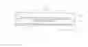
FIG. 1 is a top view of a substrate having a cavity therein.
FIG. 2 is a cross-sectional representation of the substrate in FIG. 1, having the cavity therein.
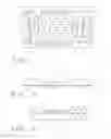
FIG. 3 is a cross-sectional representation of a die stack showing die to die interconnection.
FIG. 4 is a cross-sectional representation of a flip chip attachment of the substrate and the die stack of FIGS. 2 and 3, respectively.
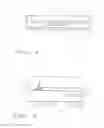
FIG. 5 is an enlarged cross-sectional representation of a portion of FIG. 4.
DETAILED DESCRIPTION
The present disclosure is a process integration method of fabricating chip on chip using flip chip attachment and a cavity substrate. For example, this method can be used for passive and power management integrated circuit (PMIC) devices. The Daughter die, such as an integrated passive device (IPD) chip, is attached under the Mother die, such as a power management chip, resulting in an inverted pyramid die stack once flipped onto the cavity substrate. Since the daughter chip protrudes below the interconnects of the mother chip, it needs a cavity substrate for flip chip attachment. The die on die attach capability produces direct contact between the mother and daughter chips.
This package technology has recently become viable due to:
1) Availability of the IPD die, and
2) Laminate cavity substrate as opposed to the use of standard surface mount passives.
Higher accuracy drilling capabilities of substrate suppliers are essential to this technology. Higher drilling accuracy minimizes cavity sizes to prevent potential package XY dimension increase for integration into existing products. Package XY dimension is critical in order to reduce end printed circuit board (PCB) space which is at a premium and very cost sensitive.
Advancements in substrate drilling systems and tools prevent mechanical vibration resulting in mechanical damage and substrate layer separation which can lead to package delamination and reliability failures and permits the laser drilling of cavities in laminate substrates.
Referring now more particularly to FIGS. 1-5, a preferred integration method will be described.
The present disclosure provides a new process integration for fabricating chip on chip using flip chip attachment and a cavity substrate. For example, these may be passive and power management integrated circuit (PMIC) devices, but the method is not limited to only these types of devices. For illustration purposes, the mother chip will be a power management chip and the daughter chip will be an integrated passive device, for example.
Referring now to FIG. 3, there is shown
-
- 1) Mother chip 10, which may be a power management chip.
- 2) Daughter chip 14, which may be an IPD chip.
- 3) Active surface of the IPD chip 16 being attached to the active surface of the power management chip 12 using micro bump 33.
- 4) The copper pillar interconnect 35 for the power management chip to attach the pyramid die stack to the laminate substrate 20 (FIG. 2).
The IPD chip could be a capacitor array or other passives such as resistors, inductors, baluns, or filters, or the like. The direct electrical connections between the active surfaces of the two dies 10 and 14, using micro bump 33, result in better electrical performance than non-direct connections, such as wire bonding or passive surface mount and connection via laminate substrate copper trace. The die on die attach results in the flip chip attach of the pyramid die stack as shown in FIG. 4.
The IPD die is smaller than the PMIC die in all dimensions, i.e. length, width, and height directions. The IPD die size can vary depending upon the number of passives required. The smaller IPD die, when attached to the PMIC die, then results in a pyramid die stack configuration.
FIG. 2. illustrates a laminate substrate 20 having solder balls 30 on the underside of the substrate. Solder balls are required for BGA packages, but this cavity substrate technology is also applicable for LGA packages where solder balls are not attached. The substrate 20 has been laser drilled to form cavity 25.
Advancements in substrate drilling techniques and tools allow for the laser drilling of this small cavity 25 without increasing the package dimension and without causing mechanical damage or substrate layer separation.
FIG. 1 illustrates a top view of the substrate shown in cross-section view A-A′ in FIG. 2. Rectangular cavity 25 is shown.
The die on die attached chips shown in FIG. 3 are flipped resulting in an inverted pyramid die stack 22 as shown in FIG. 4. Now the die stack 22 is connected to the BGA substrate 20 via the copper pillars 35 using a flip chip attach method. The passive IPD die 14 protrudes below the interconnects 35 of the mother die 10. It fits into the cavity 25 drilled into the substrate 20, but is not connected to the substrate 20.
This method can be applied for some existing products by re-routing substrate metal traces in the laminate substrate to make space available for the cavity. This is only a slight change as compared to the standard substrate. Alternatively, the cavity can be designed into new laminate substrates.
FIG. 5 is an enlarged portion of the cross-section of FIG. 4. There is shown:
1) Laminate substrate 20
2) Power management chip 10.
3) IPD chip 14.
4) Power management to substrate interconnect via flip chip attach 35.
5) IPD to power management interconnect micro bumps 33.
6) Flip Chip attach first underfill 32.
7) Epoxy Molding Compound 34.
8) Substrate cavity 25 filled with second underfill.
9) BGA solder balls 30.
Although the preferred embodiment of the present disclosure has been illustrated, and that form has been described in detail, it will be readily understood by those skilled in the art that various modifications may be made therein without departing from the spirit of the disclosure or from the scope of the appended claims.
Claims
What is claimed is:1. A method of fabricating a mother and daughter integrated circuit device comprising:
providing a mother die having an active surface;
providing a daughter die having an active surface wherein said daughter die is smaller than said mother die in all dimensions;
directly connecting said active surface of said daughter die to said active surface of said mother die by micro-bumps resulting in a pyramid die stack;
providing a laminate substrate having a rectangular cavity drilled therein wherein said cavity corresponds to a size and position of said daughter die in relation to said mother die, and wherein there is no opening into said cavity from an opposite side of said substrate; and
attaching said pyramid die stack to said substrate by copper pillars using a flip chip method wherein said daughter die fits into said cavity, wherein said daughter die is not attached to said substrate, but is surrounded by said cavity, and wherein a first underfill surrounds said mother die, and wherein a second underfill fills said cavity around said daughter die.
2. The method according to claim 1 wherein said mother die is a power management circuit chip.
3. The method according to claim 1 wherein said daughter die is an integrated passive device containing at least one passive device.
4. The method according to claim 3 wherein said at least one passive device is chosen from the group containing a capacitor, a resistor, an inductor, a balun, and a filter.
5. The method according to claim 1 wherein said cavity is drilled by a mechanical drilling process or a laser drilling process.
6. The method according to claim 1 wherein said substrate is a ball grid array or a land grid array substrate.
7. A method of fabricating an integrated passive device comprising:
providing a first die containing at least one power management device;
providing a second die containing at least one passive device wherein said second die is smaller than said first die;
directly connecting an active surface of said second die to an active surface of said first die resulting in a die stack;
providing a substrate having a rectangular cavity drilled therein wherein said cavity corresponds to a size and position of said second die in relation to said first die;
attaching said die stack to said substrate using a flip chip method wherein said second die fits into said cavity, wherein said second die is not attached to said substrate, but is surrounded by said cavity;
providing a first underfill surrounding said first die;
thereafter providing a second underfill filling said savity around said second die; and
thereafter coating an epoxy molding compound over said die stack.
8. The method according to claim 7 wherein said at least one passive device is chosen from the group containing a capacitor, a resistor, an inductor, a balun, and a filter.
9. The method according to claim 7 wherein said directly connecting said active surface of said second die to said active surface of said first die comprises micro bumps.
10. The method according to claim 7 wherein said cavity is drilled by a mechanical drilling process or by a laser drilling process.
11. The method according to claim 7 wherein said substrate is a ball grid array or a land grid array substrate.
12. The method according to claim 7 wherein said attaching said die stack to said substrate comprises copper pillar interconnects.
13. A method of fabricating an integrated passive device comprising:
providing a first die and a second die wherein said second die is smaller than said first die in all dimensions;
directly connecting an active surface of said second die to an active surface of said first die resulting in a die stack;
providing a substrate having a rectangular cavity laser drilled therein wherein said cavity corresponds to a size and position of said second die in relation to said first die;
attaching said die stack to said substrate using a flip chip method wherein said second die fits into said cavity, wherein said second die is not attached to said substrate, but is surrounded by said cavity;
providing a first underfill surrounding said first die;
thereafter providing a second underfill filling said cavity around said second die; and
thereafter coating an epoxy molding compound over said die stack.
14. The method according to claim 13 wherein said first die is a power management circuit chip.
15. The method according to claim 13 wherein said second die is an integrated passive device containing at least one passive device.
16. The method according to claim 15 wherein said at least one passive device is chosen from the group containing a capacitor, a resistor, an inductor, a balun, and a filter.
17. The method according to claim 13 wherein said directly connecting said active surface of said second die to said active surface of said first die comprises micro bumps.
18. The method according to claim 13 wherein said substrate is a ball grid array or a land grid array substrate.
19. The method according to claim 13 wherein said attaching said die stack to said substrate comprises copper pillar interconnects.
20. The method according to claim 13 wherein said substrate is a laminate substrate having a Bismaleimide Triazine (BT) core.
Images & Drawings included:
Sources:
- United States Patent and Trademark Office - verify current appl. status at the USPTO↗
Similar patent applications:
Recent applications in this class:
- » 20250293227 2025-09-18
HYBRID RECONSTITUTED PANEL LEVEL PACKAGING - » 20250279405 2025-09-04
POWER MODULE PACKAGE FOR DIRECT COOLING MULTIPLE POWER MODULES - » 20250266417 2025-08-21
SEMICONDUCTOR STRUCTURE AND MANUFACTURING METHOD THEREOF - » 20250266416 2025-08-21
STACKED DIES AND METHODS FOR FORMING BONDED STRUCTURES - » 20250246590 2025-07-31
INTEGRATED DEVICES HAVING MULTIPLE DIE ORIENTATIONS - » 20250233119 2025-07-17
INTEGRATED CIRCUIT PACKAGE AND METHOD OF FORMING SAME - » 20250219043 2025-07-03
SEMICONDUCTOR PACKAGING METHOD, SEMICONDUCTOR ASSEMBLY COMPONENT AND ELECTRONIC DEVICE - » 20250210614 2025-06-26
SEMICONDUCTOR STRUCTURE AND MANUFACTURING METHOD OF THE SAME - » 20250210613 2025-06-26
DIRECT APPLIED INTERPOSER FOR CO-PACKAGED OPTICS - » 20250201798 2025-06-19
PACKAGE STRUCTURE, DIE STRUCTURE AND METHOD FOR FORMING THE PACKAGE STRUCTURE
Recent applications for this Assignee:
- » 20180150091 2018-05-31
Method and apparatus for DC-DC converter with boost/low dropout (LDO) mode control - » 20170122987 2017-05-04
Highly accurate current measurement - » 20160352352 2016-12-01
IMPROVING THE ACCURACY OF AN EXPONENTIAL CURRENT DIGITAL-TO-ANALOG CONVERTER (IDAC) USING A BINARY-WEIGHTED MSB - » 20160329812 2016-11-10
Control circuit for multiple high side switches - » 20160195884 2016-07-07
Circuits and method for controlling transient fault conditions in a low dropout voltage regulator - » 20160134196 2016-05-12
Converter one pin sensing - » 20160134183 2016-05-12
VCC charge and free-wheeling detection via source controlled MOS transistor - » 20160132064 2016-05-12
Load transient, reduced bond wires for circuits supplying large currents - » 20160094208 2016-03-31
Dynamic level shifter circuit - » 20160070291 2016-03-10
Static offset reduction in a current conveyor