Wrap-around contact integration scheme
US20170345904A1
2017-11-30
15/604,399
2017-05-24
✅ Patent granted
US 10,381,448 B2
2019-08-13
-
-
Alexander O Williams
2037-05-24
Abstract:
Embodiments of the invention provide a wrap-around contact integration scheme that includes sidewall protection during contact formation. A substrate processing method includes providing a substrate containing a raised contact in a first dielectric film, and a second dielectric film on the first dielectric film, where the second dielectric film has a recessed feature with a sidewall and a bottom portion above the raised contact. The method further includes depositing a conformal film on the sidewall and on the bottom portion of the recessed feature, removing the conformal film from the bottom portion in a first anisotropic etching process, where the remaining conformal film forms a protection film on the sidewall and defines a width of the recessed feature, and forming a cavity containing the raised contact in an isotropic etching process, where a width of the cavity is greater than the width of the recessed feature.
Inventors:
- Robert D. Clark 35 🇺🇸 Livermore, CA, United States
- Kandabara N. Tapily 31 🇺🇸 Mechanicville, NY, United States
Assignee:
- TOKYO ELECTRON LIMITED 9,708 🇯🇵 Tokyo, Japan
Applicant:
Interested in similar patents?
Get notified when new applications in this technology area are published.
Classification:
H01L29/41791 » CPC main
Semiconductor devices adapted for rectifying, amplifying, oscillating or switching, or capacitors or resistors with at least one potential-jump barrier or surface barrier, e.g. PN junction depletion layer or carrier concentration layer; Details of semiconductor bodies or of electrodes thereof; Multistep manufacturing processes therefor; Electrodes ; Multistep manufacturing processes therefor characterised by their shape, relative sizes or dispositions carrying the current to be rectified, amplified or switched; Source or drain electrodes for field effect devices for transistors with a horizontal current flow in a vertical sidewall, e.g. FinFET, MuGFET
H01L21/76802 » CPC further
Processes or apparatus adapted for the manufacture or treatment of semiconductor or solid state devices or of parts thereof; Manufacture or treatment of devices consisting of a plurality of solid state components formed in or on a common substrate or of parts thereof; Manufacture of integrated circuit devices or of parts thereof; Manufacture of specific parts of devices defined in group; Applying interconnections to be used for carrying current between separate components within a device comprising conductors and dielectrics characterised by the formation and the after-treatment of the dielectrics, e.g. smoothing by forming openings in dielectrics
H01L21/76843 » CPC further
Processes or apparatus adapted for the manufacture or treatment of semiconductor or solid state devices or of parts thereof; Manufacture or treatment of devices consisting of a plurality of solid state components formed in or on a common substrate or of parts thereof; Manufacture of integrated circuit devices or of parts thereof; Manufacture of specific parts of devices defined in group; Applying interconnections to be used for carrying current between separate components within a device comprising conductors and dielectrics characterised by the formation and the after-treatment of the conductors; Barrier, adhesion or liner layers formed in openings in a dielectric
H01L21/76877 » CPC further
Processes or apparatus adapted for the manufacture or treatment of semiconductor or solid state devices or of parts thereof; Manufacture or treatment of devices consisting of a plurality of solid state components formed in or on a common substrate or of parts thereof; Manufacture of integrated circuit devices or of parts thereof; Manufacture of specific parts of devices defined in group; Applying interconnections to be used for carrying current between separate components within a device comprising conductors and dielectrics characterised by the formation and the after-treatment of the conductors Filling of holes, grooves or trenches, e.g. vias, with conductive material
H01L29/1608 » CPC further
Semiconductor devices adapted for rectifying, amplifying, oscillating or switching, or capacitors or resistors with at least one potential-jump barrier or surface barrier, e.g. PN junction depletion layer or carrier concentration layer; Details of semiconductor bodies or of electrodes thereof; Multistep manufacturing processes therefor; Semiconductor bodies ; Multistep manufacturing processes therefor characterised by the materials of which they are formed including, apart from doping materials or other impurities, only elements of Group IV of the Periodic System Silicon carbide
H01L29/66 IPC
Semiconductor devices adapted for rectifying, amplifying, oscillating or switching, or capacitors or resistors with at least one potential-jump barrier or surface barrier, e.g. PN junction depletion layer or carrier concentration layer; Details of semiconductor bodies or of electrodes thereof; Multistep manufacturing processes therefor Types of semiconductor device ; Multistep manufacturing processes therefor
H01L21/02 IPC
Processes or apparatus adapted for the manufacture or treatment of semiconductor or solid state devices or of parts thereof Manufacture or treatment of semiconductor devices or of parts thereof
H01L29/16 IPC
Semiconductor devices adapted for rectifying, amplifying, oscillating or switching, or capacitors or resistors with at least one potential-jump barrier or surface barrier, e.g. PN junction depletion layer or carrier concentration layer; Details of semiconductor bodies or of electrodes thereof; Multistep manufacturing processes therefor; Semiconductor bodies ; Multistep manufacturing processes therefor characterised by the materials of which they are formed including, apart from doping materials or other impurities, only elements of Group IV of the Periodic System
H01L29/45 » CPC further
Semiconductor devices adapted for rectifying, amplifying, oscillating or switching, or capacitors or resistors with at least one potential-jump barrier or surface barrier, e.g. PN junction depletion layer or carrier concentration layer; Details of semiconductor bodies or of electrodes thereof; Multistep manufacturing processes therefor; Electrodes ; Multistep manufacturing processes therefor characterised by the materials of which they are formed Ohmic electrodes
H01L29/78 IPC
Semiconductor devices adapted for rectifying, amplifying, oscillating or switching, or capacitors or resistors with at least one potential-jump barrier or surface barrier, e.g. PN junction depletion layer or carrier concentration layer; Details of semiconductor bodies or of electrodes thereof; Multistep manufacturing processes therefor; Types of semiconductor device ; Multistep manufacturing processes therefor controllable by only the electric current supplied, or only the electric potential applied, to an electrode which does not carry the current to be rectified, amplified or switched; Unipolar devices, e.g. field effect transistors; Field effect transistors with field effect produced by an insulated gate
H01L21/768 IPC
Processes or apparatus adapted for the manufacture or treatment of semiconductor or solid state devices or of parts thereof; Manufacture or treatment of devices consisting of a plurality of solid state components formed in or on a common substrate or of parts thereof; Manufacture of integrated circuit devices or of parts thereof; Manufacture of specific parts of devices defined in group Applying interconnections to be used for carrying current between separate components within a device comprising conductors and dielectrics
H01L29/161 » CPC further
Semiconductor devices adapted for rectifying, amplifying, oscillating or switching, or capacitors or resistors with at least one potential-jump barrier or surface barrier, e.g. PN junction depletion layer or carrier concentration layer; Details of semiconductor bodies or of electrodes thereof; Multistep manufacturing processes therefor; Semiconductor bodies ; Multistep manufacturing processes therefor characterised by the materials of which they are formed including, apart from doping materials or other impurities, only elements of Group IV of the Periodic System including two or more of the elements provided for in group , e.g. alloys
H01L21/76816 » CPC further
Processes or apparatus adapted for the manufacture or treatment of semiconductor or solid state devices or of parts thereof; Manufacture or treatment of devices consisting of a plurality of solid state components formed in or on a common substrate or of parts thereof; Manufacture of integrated circuit devices or of parts thereof; Manufacture of specific parts of devices defined in group; Applying interconnections to be used for carrying current between separate components within a device comprising conductors and dielectrics characterised by the formation and the after-treatment of the dielectrics, e.g. smoothing by forming openings in dielectrics Aspects relating to the layout of the pattern or to the size of vias or trenches
H01L21/76831 » CPC further
Processes or apparatus adapted for the manufacture or treatment of semiconductor or solid state devices or of parts thereof; Manufacture or treatment of devices consisting of a plurality of solid state components formed in or on a common substrate or of parts thereof; Manufacture of integrated circuit devices or of parts thereof; Manufacture of specific parts of devices defined in group; Applying interconnections to be used for carrying current between separate components within a device comprising conductors and dielectrics characterised by the formation and the after-treatment of the dielectrics, e.g. smoothing characterised by the formation of thin functional dielectric layers, e.g. dielectric etch-stop, barrier, capping or liner layers in via holes or trenches, e.g. non-conductive sidewall liners
H01L29/41783 » CPC further
Semiconductor devices adapted for rectifying, amplifying, oscillating or switching, or capacitors or resistors with at least one potential-jump barrier or surface barrier, e.g. PN junction depletion layer or carrier concentration layer; Details of semiconductor bodies or of electrodes thereof; Multistep manufacturing processes therefor; Electrodes ; Multistep manufacturing processes therefor characterised by their shape, relative sizes or dispositions carrying the current to be rectified, amplified or switched; Source or drain electrodes for field effect devices characterised by the proximity or the relative position of the source or drain electrode and the gate electrode, e.g. the source or drain electrode separated from the gate electrode by side-walls or spreading around or above the gate electrode Raised source or drain electrodes self aligned with the gate
H01L23/485 » CPC further
Details of semiconductor or other solid state devices; Arrangements for conducting electric current to or from the solid state body in operation, e.g. leads, terminal arrangements ; Selection of materials therefor consisting of lead-in layers inseparably applied to the semiconductor body consisting of layered constructions comprising conductive layers and insulating layers, e.g. planar contacts
H01L29/417 IPC
Semiconductor devices adapted for rectifying, amplifying, oscillating or switching, or capacitors or resistors with at least one potential-jump barrier or surface barrier, e.g. PN junction depletion layer or carrier concentration layer; Details of semiconductor bodies or of electrodes thereof; Multistep manufacturing processes therefor; Electrodes ; Multistep manufacturing processes therefor characterised by their shape, relative sizes or dispositions carrying the current to be rectified, amplified or switched
Description
CROSS-REFERENCE TO RELATED APPLICATIONS
This application is related to and claims priority to U.S. Provisional Patent Application Ser. No. 62/341,807 filed on May 26, 2016, the entire contents of which are herein incorporated by reference.
FIELD OF INVENTION
The present invention relates to the field of semiconductor manufacturing and semiconductor devices, and more particularly, to a wrap-around contact integration scheme that includes sidewall protection during contact formation.
BACKGROUND OF THE INVENTION
Current and future generations of metal-oxide-semiconductor field-effect transistors (MOSFETs) require tight control of parasitic capacitance while simultaneously optimizing metal-semiconductor contact resistance. In FinFET structures, maximizing the contact area can be achieved by creating a contact that wraps around the fin or by growing faceted epitaxial contacts, and then wrapping metal around the faceted epitaxial contacts. The adoption of ultra-thin transistor body structures such as FinFET and fully depleted silicon-on-insulator (FDSOI) has exacerbated the problem for logic manufacturing. In order to reduce contact resistance in FinFET structures, device makers are contemplating Wrap-Around Contact (WAC) structures that allow metal-semiconductor contacts with increased area.
SUMMARY OF THE INVENTION
Embodiments of the invention provide a wrap-around contact integration scheme that includes sidewall protection during contact formation. According to one embodiment, a substrate processing method includes providing a substrate containing a raised contact in a first dielectric film, and a second dielectric film on the first dielectric film, where the second dielectric film has a recessed feature with a sidewall and a bottom portion above the raised contact. The method further includes depositing a conformal film on the sidewall and on the bottom portion of the recessed feature, removing the conformal film from the bottom portion in a first anisotropic etching process, where the remaining conformal film forms a protection film on the sidewall and defines a width of the recessed feature, and forming a cavity containing the raised contact in an isotropic etching process, where a width of the cavity is greater than the width of the recessed feature.
According to one embodiment, the substrate processing method includes providing a substrate containing a raised contact in a first dielectric film, and a second dielectric film on the first dielectric film, where the second dielectric film has a recessed feature with a sidewall and a bottom portion above the raised contact. The method further includes depositing a conformal metal oxide film on the sidewall and on the bottom portion, removing the conformal film from the bottom portion in a first anisotropic etching process, where the remaining conformal film forms a protection film on the sidewall and defines a width of the recessed feature, extending the recessed feature to the raised contact using a second anisotropic etching process, forming a cavity containing the raised contact in an isotropic etching process, where a width of the cavity is greater than the width of the recessed feature, and filling the recessed feature and the cavity with a metal.
According to one embodiment, semiconductor device is described that includes a substrate containing a raised contact in a cavity in a first dielectric film, and a second dielectric film on the first dielectric film, where the second dielectric film has a recessed feature with a sidewall above the raised contact, a protection film on the sidewall, the protection film defining a width of the recessed feature, and a metal filling the cavity and the recessed feature, wherein a width of the cavity is greater than the width of the recessed feature.
BRIEF DESCRIPTION OF THE DRAWINGS
A more complete appreciation of the invention and many of the attendant advantages thereof will be readily obtained as the same becomes better understood by reference to the following detailed description when considered in connection with the accompanying drawings, wherein:
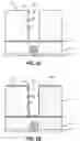
FIG. 1 is a process flow diagram for a method of processing a substrate according to an embodiment of the invention; and
FIGS. 2A-2G schematically show through cross-sectional views a method of processing a substrate according to an embodiment of the invention.
DETAILED DESCRIPTION OF SEVERAL EMBODIMENTS
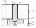
FIG. 1 is a process flow 1 for a method of processing a substrate according to an embodiment of the invention, and FIGS. 2A-2G schematically show through cross-sectional views a method of processing a substrate according to an embodiment of the invention. The method includes, in 100, providing a substrate containing a raised contact 216 in a first dielectric film 200, and a second dielectric film 202 on the first dielectric film 200, where the second dielectric film 202 has a recessed feature 204 with a sidewall 201 and a bottom portion 203 above the raised contact 216. The substrate further includes an etch stop layer 212 on the first dielectric film 200, and a dielectric film 218 underneath the first dielectric film 200. The etch stop layer 212 may be used to terminate the etching during the formation of the recessed feature 204. The etch stop layer 212 may, for example, include a high-k material, silicon nitride, silicon oxide, carbon, or silicon.
The recessed feature 204 can, for example, have a width 207 that is less than 200 nm, less than 100 nm, less than 50 nm, less than 25 nm, less than 20 nm, or less than 10 nm. In other examples, the recessed feature 204 can have a width 207 that is between 5 nm and 10 nm, between 10 nm and 20 nm, between 20 nm and 50 nm, between 50 nm and 100 nm, between 100 nm and 200 nm, between 10 nm and 50 nm, or between 10 nm and 100 nm. The width 207 can also be referred to as a critical dimension (CD). The recessed feature 204 can, for example, have a depth of 25 nm, 50 nm, 100 nm, 200 nm, or greater than 200 nm. In some examples, the first dielectric film 200 may contain SiO2, SiON, SiN, a high-k material, a low-k material, or an ultra-low-k material. In some examples, the second dielectric film 202 may contain SiO2, SiON, SiN, a high-k material, a low-k material, or an ultra-low-k material. In one example, the raised contact includes SiGe or SiC.
The recessed feature 204 in the second dielectric film 202 may be formed using well-known lithography and etching processes. Although not shown in FIG. 2A, a patterned mask layer may be present on the field area 211 and defining the opening of the recessed feature 204.
The process flow 1 further includes, in 102, depositing a conformal film 208 on the sidewall 201 and on the bottom portion 203. This is schematically shown in FIG. 2B. According to one embodiment, the conformal film 208 may be deposited by atomic layer deposition (ALD). ALD can deposit very thin films with atomic level thickness control and excellent conformality over advanced raised and recessed features. According to one embodiment, the conformal film 208 can include a metal oxide film. The metal oxide film can be a high-k film. In one example, the metal oxide film may be selected from the group consisting of HfO2, ZrO2, TiO2, Al2O3, and a combination thereof. However, other metal oxide films may be used. According to another embodiment, the conformal film 208 may be selected from the group consisting of a metal oxide film, a metal nitride film, a metal oxynitride film, a metal silicate film, and a combination thereof.
In one example, the conformal film 208 includes a metal oxide film that is deposited using ALD by a) pulsing a metal-containing precursor into a process chamber containing the substrate, b) purging the process chamber with an inert gas; c) pulsing an oxygen-containing precursor into the process chamber, d) purging the process chamber with an inert gas, and e) repeating a)-d) at least once.
A thickness of the conformal film 208 may be selected to provide adequate protection against etching of the sidewall 201 during a) a cleaning process that may be carried out to remove residue from the recessed feature 204, and/or b) during etching of the etch stop layer 212 and the first dielectric film 200. In some examples, a thickness of the conformal film 208 can be 10 nm or less, 5 nm or less, 4 nm or less, between 1 nm and 2 nm, between 2 nm and 4 nm, between 4 nm and 6 nm, between 6 nm and 8 nm, or between 2 nm and 6 nm. The presence of the conformal film 208 on the sidewall 201 reduces the width 207 of the recessed feature 204 to a width 209. However, this change in width can be relatively small since the conformal film 208 may be only a few nm thick.
The process flow 1 further includes, in 104, removing the conformal film 208 from the bottom portion 203 in a first anisotropic etching process, where the remaining conformal film forms a protection film 214 on the sidewall 201 of the recessed feature 204. This is schematically shown in FIG. 2C. The first anisotropic etching process may utilize a dry etching process that is directional and thus etches the conformal film 208 faster from the field area 211 and the bottom portion 203 than from the sidewall 201. In one example, the first anisotropic etching process can include a digital etching process or a plasma-enhanced atomic layer etching (PEALE). According to one embodiment, the first anisotropic etching process can include alternating exposures of BCl3 gas and plasma-excited argon gas. The first anisotropic etching process forms a recess 205 in the first dielectric film 200 following the removal of the conformal film 208 from the bottom portion 203. This is schematically shown in FIG. 2C.
The method further includes extending the recessed feature 204 to the raised contact 216 in the first dielectric film 200 using a second anisotropic etching process. This is schematically shown in FIG. 2D. The protection film 214 has adequate thickness and etch resistance to prevent or reduce etching of the sidewall 201 during the second anisotropic etching process, thus preventing loss of critical dimension.
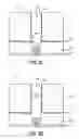
The process flow 1 further includes, in 106, forming a cavity 210 containing the raised contact 216 in an isotropic etching process, where a width 211 of the cavity 210 is greater than the width 209 of the recessed feature 204. This is schematically shown in FIG. 2E. In one example, the isotropic etching process can include thermal atomic layer etching (ALE).
According to one embodiment, the method can further include depositing a barrier layer 220 on the protection film 214 in the recessed feature 204 and on surfaces in the cavity 210. In one example, the barrier layer 220 can include a Ti layer, a TiN layer, or both a Ti layer and a TiN layer. This is schematically shown in FIG. 2F.
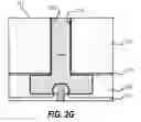
According to one embodiment, the method further includes filling the recessed feature 204 and the cavity 210 with a metal 222 that wraps around the raised contact 216. The metal may, for example, be selected from the group consisting of tungsten (W) and copper (Cu). This is schematically shown in FIG. 2G.
According to one embodiment, the protection film 214 may be removed from the recessed feature 204 prior to depositing a barrier layer and filling the recessed feature with the metal 222. According to one embodiment, the protection film 214 may be removed using an exposure of BCl3 gas and plasma-excited argon gas.
A wrap-around contact integration scheme that includes sidewall protection during contact formation has been disclosed in various embodiments. The foregoing description of the embodiments of the invention has been presented for the purposes of illustration and description. It is not intended to be exhaustive or to limit the invention to the precise forms disclosed. This description and the claims following include terms that are used for descriptive purposes only and are not to be construed as limiting. Persons skilled in the relevant art can appreciate that many modifications and variations are possible in light of the above teaching. Persons skilled in the art will recognize various equivalent combinations and substitutions for various components shown in the Figures. It is therefore intended that the scope of the invention be limited not by this detailed description, but rather by the claims appended hereto.
Claims
What is claimed is:1. A substrate processing method, comprising:
providing a substrate containing a raised contact in a first dielectric film, and a second dielectric film on the first dielectric film, wherein the second dielectric film has a recessed feature with a sidewall and a bottom portion above the raised contact;
depositing a conformal film on the sidewall and on the bottom portion of the recessed feature;
removing the conformal film from the bottom portion in a first anisotropic etching process, wherein the remaining conformal film forms a protection film on the sidewall and defines a width of the recessed feature; and
forming a cavity containing the raised contact in an isotropic etching process, wherein a width of the cavity is greater than the width of the recessed feature.
2. The method of claim 1, further comprising:
prior to forming the cavity, extending the recessed feature to the raised contact in the first dielectric film using a second anisotropic etching process.
3. The method of claim 1, further comprising:
depositing barrier layer in the recessed feature and in the cavity.
4. The method of claim 3, wherein the barrier layer includes a Ti layer, a TiN layer, or both a Ti layer and a TiN layer.
5. The method of claim 1, further comprising:
filling the recessed feature and the cavity with a metal.
6. The method of claim 5, wherein the metal is selected from the group consisting of tungsten (W) and copper (Cu).
7. The method of claim 5, further comprising:
prior to the filling, removing the protection film from the recessed feature.
8. The method of claim 1, wherein the first dielectric film, the second dielectric film, or both the first and second dielectric films, include SiO2.
9. The method of claim 1, wherein the conformal film includes a metal oxide film selected from the group consisting of HfO2, ZrO2, TiO2, Al2O3, and a combination thereof.
10. The method of claim 1, wherein the conformal film is selected from the group consisting of a metal oxide film, a metal nitride film, a metal oxynitride film, a metal silicate film, and a combination thereof.
11. The method of claim 1, wherein the raised contact includes SiGe or SiC.
12. A substrate processing method, comprising:
providing a substrate containing a raised contact in a first dielectric film, and a second dielectric film on the first dielectric film, wherein the second dielectric film has a recessed feature with a sidewall and a bottom portion above the raised contact;
depositing a conformal metal oxide film on the sidewall and on the bottom portion;
removing the conformal film from the bottom portion in a first anisotropic etching process, wherein the remaining conformal film forms a protection film on the sidewall and defines a width of the recessed feature;
extending the recessed feature to the raised contact using a second anisotropic etching process;
forming a cavity containing the raised contact in an isotropic etching process, wherein a width of the cavity is greater than the width of the recessed feature; and
filling the recessed feature and the cavity with a metal.
13. A semiconductor device, comprising:
a substrate containing a raised contact in a cavity in a first dielectric film, and a second dielectric film on the first dielectric film, wherein the second dielectric film has a recessed feature with a sidewall above the raised contact;
a protection film on the sidewall, the protection film defining a width of the recessed feature; and
a metal filling the cavity and the recessed feature, wherein a width of the cavity is greater than the width of the recessed feature.
14. The semiconductor device of claim 13, further comprising:
a barrier layer in the recessed feature and in the cavity.
15. The semiconductor device of claim 14, wherein the barrier layer includes a Ti layer, a TiN layer, or both a Ti layer and a TiN layer.
16. The semiconductor device of claim 13, wherein the metal is selected from the group consisting of tungsten (W) or copper (Cu).
17. The semiconductor device of claim 13, wherein the first dielectric film, the second dielectric film, or both the first and second dielectric films, include SiO2.
18. The semiconductor device of claim 13, wherein the protection film includes a metal oxide film selected from the group consisting of HfO2, ZrO2, TiO2, Al2O3, and a combination thereof.
19. The semiconductor device of claim 13, wherein the conformal film is selected from the group consisting of a metal oxide film, a metal nitride film, a metal oxynitride film, a metal silicate film, and a combination thereof.
20. The semiconductor device of claim 13, wherein the raised contact includes SiGe or SiC.
Images & Drawings included:

Sources:
- United States Patent and Trademark Office - verify current appl. status at the USPTO↗
Similar patent applications:
- » 20180068899
Wrap-around contact integration scheme
Recent applications in this class:
- » 20250056832 2025-02-13
SEMICONDUCTOR DEVICE AND METHOD - » 20250031404 2025-01-23
SEMICONDUCTOR DEVICE AND METHODS OF FORMATION - » 20250031403 2025-01-23
CONTACT PLUG STRUCTURES OF SEMICONDUCTOR DEVICE AND METHODS OF FORMING SAME - » 20250015154 2025-01-09
Multigate Device Having Reduced Contact Resistivity - » 20240413217 2024-12-12
SEMICONDUCTOR DEVICE STRUCTURE WITH BUTTED-CONTACT AND METHODS OF FORMING THE SAME - » 20240405087 2024-12-05
SEMICONDUCTOR DEVICE AND MANUFACTURING METHOD THEREOF - » 20240395882 2024-11-28
SEMICONDUCTOR DEVICE AND FABRICATION METHOD THEREOF - » 20240387665 2024-11-21
SEMICONDUCTOR DEVICE AND METHOD OF MANUFACTURE - » 20240387664 2024-11-21
Semiconductor Device and Method of Forming Thereof - » 20240387663 2024-11-21
SEMICONDUCTOR DEVICE STRUCTURE AND METHODS OF FORMING THE SAME
Recent applications for this Assignee:
- » 20250293095 2025-09-18
SYSTEM AND METHOD OF PULSE SCORING - » 20250293065 2025-09-18
BONDING APPARATUS AND BONDING METHOD - » 20250293058 2025-09-18
SEPARATING APPARATUS AND SEPARATING METHOD - » 20250293042 2025-09-18
HARC ETCH CHEMISTRY FOR SEMINCONDUCTORS - » 20250293010 2025-09-18
SUBSTRATE PROCESSING APPARATUS, SUBSTRATE PROCESSING SYSTEM, AND MAINTENANCE METHOD - » 20250293005 2025-09-18
PLASMA PROCESSING APPARATUS - » 20250292996 2025-09-18
PLASMA PROCESSING APPARATUS - » 20250292374 2025-09-18
METHOD OF GENERATING LEARNING MODEL, INFORMATION PROCESSING METHOD, RECORDING MEDIUM, AND INFORMATION PROCESSING DEVICE - » 20250292119 2025-09-18
RECORDING MEDIUM, INFORMATION PROCESSING APPARATUS, AND INFORMATION PROCESSING METHOD - » 20250291849 2025-09-18
RECORDING MEDIUM, INFORMATION PROCESSING APPARATUS, AND INFORMATION PROCESSING METHOD