Packaged IC With Solderable Sidewalls
US20170365575A1
2017-12-21
15/690,074
2017-08-29
Abstract:
A packaged IC wherein a portion of the sidewalls of the packaged IC are solderable metal. A method of forming a packaged IC wherein a portion of the sidewalls of the wire bond pads or the flip chip pads that are exposed by sawing during singulation are solderable metal. A method of forming a packaged IC wherein all of the sidewalls of the wire bond pads or the flip chip pads that are exposed by sawing during singulation are solderable metal and a portion of sidewall of the molding compound is solderable metal.
Inventors:
- Vikas Gupta 43 🇺🇸 Dallas, TX, United States
- Yong Lin 9 🇺🇸 Plano, TX, United States
- Rongwei Zhang 14 🇺🇸 Plano, TX, United States
Interested in similar patents?
Get notified when new applications in this technology area are published.
Classification:
H01L24/29 » CPC main
Arrangements for connecting or disconnecting semiconductor or solid-state bodies; Methods or apparatus related thereto; Means for bonding being attached to, or being formed on, the surface to be connected, e.g. chip-to-package, die-attach, "first-level" interconnects; Manufacturing methods related thereto; Layer connectors, e.g. plate connectors, solder or adhesive layers; Manufacturing methods related thereto; Structure, shape, material or disposition of the layer connectors prior to the connecting process of an individual layer connector
H01L21/4825 » CPC further
Processes or apparatus adapted for the manufacture or treatment of semiconductor or solid state devices or of parts thereof; Manufacture or treatment of semiconductor devices or of parts thereof the devices having at least one potential-jump barrier or surface barrier, e.g. PN junction, depletion layer or carrier concentration layer; Manufacture or treatment of parts, e.g. containers, prior to assembly of the devices, using processes not provided for in a single one of the subgroups -; Conductive parts; Flat leads, e.g. lead frames with or without insulating supports Connection or disconnection of other leads to or from flat leads, e.g. wires, bumps, other flat leads
H01L21/565 » CPC further
Processes or apparatus adapted for the manufacture or treatment of semiconductor or solid state devices or of parts thereof; Manufacture or treatment of semiconductor devices or of parts thereof the devices having at least one potential-jump barrier or surface barrier, e.g. PN junction, depletion layer or carrier concentration layer; Assembly of semiconductor devices using processes or apparatus not provided for in a single one of the subgroups - , e.g. sealing of a cap to a base of a container; Encapsulations, e.g. encapsulation layers, coatings Moulds
H01L23/3114 » CPC further
Details of semiconductor or other solid state devices; Encapsulations, e.g. encapsulating layers, coatings, e.g. for protection characterised by the arrangement or shape the device being completely enclosed the device being a chip scale package, e.g. CSP
H01L21/78 » CPC further
Processes or apparatus adapted for the manufacture or treatment of semiconductor or solid state devices or of parts thereof; Manufacture or treatment of devices consisting of a plurality of solid state components formed in or on a common substrate or of parts thereof; Manufacture of integrated circuit devices or of parts thereof; Manufacture or treatment of devices consisting of a plurality of solid state components or integrated circuits formed in, or on, a common substrate with subsequent division of the substrate into plural individual devices
H01L23/4952 » CPC further
Details of semiconductor or other solid state devices; Arrangements for conducting electric current to or from the solid state body in operation, e.g. leads, terminal arrangements ; Selection of materials therefor consisting of soldered constructions; Lead-frames or other flat leads; Additional leads the additional leads being a bump or a wire
H01L23/49541 » CPC further
Details of semiconductor or other solid state devices; Arrangements for conducting electric current to or from the solid state body in operation, e.g. leads, terminal arrangements ; Selection of materials therefor consisting of soldered constructions; Lead-frames or other flat leads Geometry of the lead-frame
H01L24/27 » CPC further
Arrangements for connecting or disconnecting semiconductor or solid-state bodies; Methods or apparatus related thereto; Means for bonding being attached to, or being formed on, the surface to be connected, e.g. chip-to-package, die-attach, "first-level" interconnects; Manufacturing methods related thereto; Layer connectors, e.g. plate connectors, solder or adhesive layers; Manufacturing methods related thereto Manufacturing methods
H01L23/49503 » CPC further
Details of semiconductor or other solid state devices; Arrangements for conducting electric current to or from the solid state body in operation, e.g. leads, terminal arrangements ; Selection of materials therefor consisting of soldered constructions; Lead-frames or other flat leads characterised by the die pad
H01L2223/54453 » CPC further
Details relating to semiconductor or other solid state devices covered by the group; Marks applied to semiconductor devices or parts for use prior to dicing
H01L2223/54426 » CPC further
Details relating to semiconductor or other solid state devices covered by the group; Marks applied to semiconductor devices or parts for alignment
H01L2221/68327 » CPC further
Processes or apparatus adapted for the manufacture or treatment of semiconductor or solid state devices or of parts thereof covered by; Apparatus for handling semiconductor or electric solid state devices during manufacture or treatment thereof; Apparatus for handling wafers during manufacture or treatment of semiconductor or electric solid state devices or components; Apparatus not specifically provided for elsewhere for supporting or gripping using temporarily an auxiliary support used during dicing or grinding
H01L2224/27318 » CPC further
Indexing scheme for arrangements for connecting or disconnecting semiconductor or solid-state bodies and methods related thereto as covered by; Means for bonding being attached to, or being formed on, the surface to be connected, e.g. chip-to-package, die-attach, "first-level" interconnects; Manufacturing methods related thereto; Layer connectors, e.g. plate connectors, solder or adhesive layers; Manufacturing methods related thereto; Manufacturing methods by local deposition of the material of the layer connector in liquid form by dispensing droplets
H01L2224/2732 » CPC further
Indexing scheme for arrangements for connecting or disconnecting semiconductor or solid-state bodies and methods related thereto as covered by; Means for bonding being attached to, or being formed on, the surface to be connected, e.g. chip-to-package, die-attach, "first-level" interconnects; Manufacturing methods related thereto; Layer connectors, e.g. plate connectors, solder or adhesive layers; Manufacturing methods related thereto; Manufacturing methods by local deposition of the material of the layer connector in liquid form Screen printing, i.e. using a stencil
H01L2224/27848 » CPC further
Indexing scheme for arrangements for connecting or disconnecting semiconductor or solid-state bodies and methods related thereto as covered by; Means for bonding being attached to, or being formed on, the surface to be connected, e.g. chip-to-package, die-attach, "first-level" interconnects; Manufacturing methods related thereto; Layer connectors, e.g. plate connectors, solder or adhesive layers; Manufacturing methods related thereto; Manufacturing methods; Post-treatment of the layer connector Thermal treatments, e.g. annealing, controlled cooling
H01L23/00 IPC
Details of semiconductor or other solid state devices
H01L21/56 IPC
Processes or apparatus adapted for the manufacture or treatment of semiconductor or solid state devices or of parts thereof; Manufacture or treatment of semiconductor devices or of parts thereof the devices having at least one potential-jump barrier or surface barrier, e.g. PN junction, depletion layer or carrier concentration layer; Assembly of semiconductor devices using processes or apparatus not provided for in a single one of the subgroups - , e.g. sealing of a cap to a base of a container Encapsulations, e.g. encapsulation layers, coatings
H01L23/544 » CPC further
Details of semiconductor or other solid state devices Marks applied to semiconductor devices , e.g. registration marks,
H01L23/31 IPC
Details of semiconductor or other solid state devices; Encapsulations, e.g. encapsulating layers, coatings, e.g. for protection characterised by the arrangement or shape
H01L21/304 » CPC further
Processes or apparatus adapted for the manufacture or treatment of semiconductor or solid state devices or of parts thereof; Manufacture or treatment of semiconductor devices or of parts thereof the devices having at least one potential-jump barrier or surface barrier, e.g. PN junction, depletion layer or carrier concentration layer the devices having semiconductor bodies comprising elements of Group IV of the Periodic System or AB compounds with or without impurities, e.g. doping materials; Treatment of semiconductor bodies using processes or apparatus not provided for in groups - to change their surface-physical characteristics or shape, e.g. etching, polishing, cutting Mechanical treatment, e.g. grinding, polishing, cutting
H01L23/495 IPC
Details of semiconductor or other solid state devices; Arrangements for conducting electric current to or from the solid state body in operation, e.g. leads, terminal arrangements ; Selection of materials therefor consisting of soldered constructions Lead-frames or other flat leads
H01L21/48 IPC
Processes or apparatus adapted for the manufacture or treatment of semiconductor or solid state devices or of parts thereof; Manufacture or treatment of semiconductor devices or of parts thereof the devices having at least one potential-jump barrier or surface barrier, e.g. PN junction, depletion layer or carrier concentration layer Manufacture or treatment of parts, e.g. containers, prior to assembly of the devices, using processes not provided for in a single one of the subgroups -
Description
CROSS REFERENCE TO RELATED APPLICATIONS
This application is a Divisional of U.S. patent application Ser. No. 15/368,413 filed Dec. 2, 2016, and claims the benefit of priority to U.S. Provisional Application 62/262,568, filed Dec. 3, 2015, all of which are incorporated herein by reference in their entirety.
FIELD
Embodiments of the invention are directed, in general, to packaging of integrated circuit (IC) chips and, more specifically, forming solderable sidewalls on packaged IC chips.
DESCRIPTION OF THE VIEWS OF THE DRAWINGS
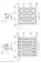
FIGS. 1A and 1B are plan views of lead frames.
FIGS. 2A and 2B are plan views of a lead frame strips.
FIGS. 3A and 3B are cross-sections of IC chips on lead frame strips prior to singulation.
FIGS. 4A, 4B, 4C, and 4D describe the attachment of a packaged IC to a circuit board by soldering.
FIGS. 5A, 5B, and 5C describe a packaged IC with solderable sidewalls formed according to embodiments.
FIGS. 6A, 6B, and 6C describe a packaged IC with solderable sidewalls formed according to embodiments.
FIGS. 7A, 7B, and 7C describe a packaged IC with solderable sidewalls formed according to embodiments.
FIGS. 8A through 8F are cross sections of the packaged IC in FIG. 6B depicted in successive stages of fabrication.
FIGS. 9A through 9E are cross sections of the packaged IC in FIG. 7B depicted in successive stages of fabrication.
DETAILED DESCRIPTION OF EXAMPLE EMBODIMENTS
Embodiments of the disclosure are described with reference to the attached figures. The figures are not drawn to scale and they are provided merely to illustrate the disclosure. Several aspects of the embodiments are described below with reference to example applications for illustration. It should be understood that numerous specific details, relationships, and methods are set forth to provide an understanding of the disclosure. One skilled in the relevant art, however, will readily recognize that the disclosure can be practiced without one or more of the specific details or with other methods. In other instances, well-known structures or operations are not shown in detail to avoid obscuring the disclosure. The embodiments are not limited by the illustrated ordering of acts or events, as some acts may occur in different orders and/or concurrently with other acts or events. Furthermore, not all illustrated acts or events are required to implement a methodology in accordance with the present disclosure.
For the purposes of this description, the term “lead frame strip” is understood to refer to a plurality of lead frames (FIG. 1A) coupled together by horizontal 202 and vertical 204 saw streets (FIG. 2A).
The term “packaged IC” is understood to refer to an IC chip attached to a lead frame and encapsulated with molding compound.
The term “solderable metal” is understood to refer to metals which solder wets readily. Examples include silver, gold, nickel, palladium, tin, solder and alloys thereof and an ink or paste comprised of a matrix containing solderable metal particles, The matrix may be a material such as a polyimide or epoxy resin or a solder flux.
Packaged ICs such as Small Outline No-Lead (SON) and Quad Flat No-Lead (QFN) ICs are typically fabricated by first attaching IC chips to a metal lead frame strip, encapsulating them with molding compound, and then singulating the encapsulated IC chips by sawing them apart along saw streets to form individual packaged ICs.
The lead frame strip 200 (FIG. 2A) for a packaged wire bonded IC 300 (FIG. 3A) is typically laid out to include for each wire bond lead frame 100 (FIG. 1A) an IC chip pad 102 and coordinated wire bond pads 104 also referred to as lead frame pads. The lead frame strip 210 (FIG. 2B) for a packaged flip chip IC 301 (FIG. 3B) is typically laid out to include for each flip chip lead frame 110 (FIG. 1B) coordinated flip chip pads 106 also referred to as lead frame pads.
In FIGS. 2A and 2B, lead frame strips, 200 and 210, are commonly formed by connecting multiple lead frames 100 or 110 together with horizontal 202 and vertical 204 saw street metal strips. These saw street metal strips, 202 and 204 are later removed by sawing (singulation) to produce individual packaged ICs.
Lead frame strips 200 and 210 are typically made of a base metal such as copper or a copper alloy. The lead frame strips, 200 and 210, may be plated with layers of solderable metal, such as a layer of nickel followed by a layer of palladium to prevent oxidation of the base metal to facilitate soldering.
A cross section of a lead frame strip 200 with attached IC chips 304 is illustrated in FIG. 3A. IC chips 304 are mounted on the IC chip pads 102 with a conductive epoxy or solder 307. In addition, IC chips 304 are electrically connected to the wire bond pads 104 with wire bonds 305. Wire bond pads 104 from adjacent lead frames 100 are attached to opposite sides of a saw street metal strip 204. The mounted IC chips 304, IC chip pads 102, wire bond pads 104 and saw street metal strips 204 are encapsulated with molding compound 308. The bottom surface 316 of the packaged wire bond IC strip 300 typically is covered with a bottom solderable metal 312 that remains exposed to enable individual packaged wire bond ICs to be soldered to a circuit board. Individual packaged wire bond ICs 400 (FIG. 4A) may then be singulated by sawing through the saw street metal strip 204 and sawing through the molding compound 308 in the saw street 205.
A cross section of a lead frame strip 210 with IC flip chips 306 is illustrated in FIG. 3B. IC flip chips 306 are integrated circuit chips that are flipped upside down and soldered to flip chip pads 106, typically using solder joints 307. Flip chip pads 106 from adjacent lead frames 110 are connected to opposite sides of a saw street metal strip 204. The IC flip chips 306, flip chip pads 106, and saw street metal strips 204 are encapsulated with molding compound 308 to form the packaged flip chip IC strip 301. The bottom surface 316 of the packaged flip chip IC strip 301 is typically covered with bottom solderable metal 314 that remains exposed to enable individual packaged flip chip ICs to be soldered to a circuit board. Individual flip chip ICs 401 (FIG. 4B) may then be singulated by sawing through the saw street metal strip 204 and sawing through the molding compound 308 in the saw street 205.
An individual packaged wire bond IC 400 after singulation is shown in FIG. 4A. The sidewall 410 of the wire bond pad 104 is exposed during the singulation process. A metal oxide 408 may form the sidewall 410 when exposed to air. This metal oxide 408 may prevent solder from wetting the sidewall 410 and forming a reliable solder joint 406.
A circuit board 402 with solder paste 405 on circuit board leads 404 is shown in FIG. 4B. In FIG. 4C, a packaged wire bond IC 400 is attached to the circuit board 402 with solder joints 406 between the circuit board leads 404 and the bottom solderable material 312 covering the bottom of the wire bond pads 104 and the IC chip pads 102.
As shown in FIG. 4C, if the oxidized metal 408 is adequately removed from the sidewall 410 prior to soldering then, a reliable solder joint 406 may be formed where the solder wets the sidewall 410 of the wire bond pad 104.
If the oxidized metal 408 is not adequately removed from the sidewall 410 of the wire bond pads 104 prior to soldering than an unreliable solder joint 407 may be formed. As is shown in FIG. 4D, the solder does not wet the sidewall 410 when the oxidized metal 408 is present. An unreliable solder joint 407 may lead to delamination of the packaged wire bond IC 400 from the circuit board 402.
FIG. 5B shows a packaged wire bond IC 500 with solderable metal 502 (metal that solder readily wets) on the sidewall of the wire bond pad 104 that is exposed during singulation. The embodiment is illustrated using a packaged wire bonded IC 500 but generally applies to all packaged ICs that are formed using lead frame strips. For example, an embodiment packaged flip chip IC with solderable metal 502 on the sidewall of the flip chip pad 106 may also be used for illustration. The solderable metal 502 may be a metal such as silver, gold, nickel, palladium, tin, solder or an alloy such as AgSn.
FIG. 5A shows a cross section of a lead frame strip 200 with packaged wire bond ICs 500 prior to singulation by sawing through the saw street 504. In this example, the saw street metal strip 204 (FIG. 3A) plus a portion of the wire bond pads 104 attached to opposite sides of the saw street metal strip 204 are replaced with solderable metal 502.
As shown in FIG. 5B the packaged wire bond IC 500 may be singulated by sawing through the saw street 504. During singulation the solderable metal 502 on the sidewalls of the wire bond pads 104 is exposed. As shown in FIG. 5C, solder wets this solderable metal 502 forming a strong solder joint 406 between the solderable metal 502, the bottom solderable metal 312 covering the bottom of the wire bond pad 104, and the lead 404 on the circuit board 402.
FIG. 6B shows a packaged wire bond IC 600 with a first solderable metal 606 on the sidewall of the wire bond pad 104 that is exposed during singulation and also with a second solderable metal 608 on a portion of the sidewall of the molding compound 308 that is exposed during singulation.
FIG. 6A shows a cross section of a lead frame strip 200 with packaged wire bond ICs 600 prior to singulation by sawing through the saw street 604. In this example, the saw street metal strip 204 (FIG. 3A) plus a portion of the wire bond pads 104 attached to opposite sides of the saw street metal strip 204 is replaced with a first solderable metal 606 forming a first solderable sidewall. In addition, a portion of the molding compound 308 in the saw street 604 and a portion of the molding compound on opposite sides of the saw street 604 are replaced with a second solderable metal 608 forming a second solderable sidewall.
After singulation by sawing, as shown in FIG. 6B, the exposed sidewall of the packaged wire bond IC 600 is comprised primarily of first and second solderable metals, 606 and 608. These solderable metals, 606 and 608, readily wet and form strong solder joints 406 when the packaged wire bond IC 600 is attached to a circuit board 402 as shown in FIG. 6C. The first solderable sidewall formed of the first solder metal 606 plus the second solderable sidewall formed of the second solderable metal 608 provides an increased area for the solder to wet thus facilitating the formation of a larger and more robust solder joint 406 as is illustrated in FIG. 6C.
For illustration two different solderable metals, 606 and 608 are used to form a sidewall on a portion of the wire bond pad 104 and to form a sidewall on a portion of the molding compound 308. Alternatively, the first and second solderable metals, 606 and 608, may be the same solderable metal. One solderable metal that adheres to both the wire bond pad 104 and to the molding compound 308 may be used. An example ink or solderable screen print paste may have solderable metal particles suspended in a polyimide or epoxy resin or in a solder flux.
FIGS. 7A-7C illustrate an example where greater than about 0% and less than about 100% of the sidewall of the wire bond pad 104 that is exposed during singulation is covered with solderable metal 702. Unlike in FIGS. 5A and 6A where the wire bond pads are completely sawed through and replaced with a solderable metal; in this embodiment the saw street metal strip 204 and the wire bond pads 104 on opposite sides of the saw street metal strip 204 are partially sawed through and replaced with a solderable metal 702. Therefore, a partial saw street metal strip 704 remains between the wire bond pads 104. The partial saw street metal strip 704 preserves the adhesive bond between the molding compound 308, the solderable metal 702, and the wire bond pads 104 during encapsulation. The partial saw street metal strip 704 may also provide reinforcement that may reduce warpage during handing.
A method for forming the embodiment packaged wire bond IC 600 shown in FIG. 6C is described in the cross sections illustrating the major processing steps in FIGS. 8A through 8F. The embodiment is illustrated with a packaged wire bonded IC 600 but it generally applies to other packaged ICs such as packaged flip chip ICs.
FIG. 8A shows two packaged wire bond is 600. IC chips 304 are mounted on IC chip pads 102 in lead frame strip 200. Wire bonds 305 electrically connect the IC chips 304 to wire bond pads 104 also in the lead frame strip 200. Wire bond pads 104 from two adjacent lead frames 100 (FIG. 1A) are attached to opposite sides of the saw street metal strip 204. The IC chips 304, the wire bonds 305, the IC chip pads 102, the wire bond pads 104, and the saw street metal strips 204 are encapsulated in molding compound 308.
In FIG. 8B a trench 805 is cut through the saw street metal strip 204 and cut through portion of the wire bond pads 104 attached on opposite sides of the saw street metal strip 204. The trench 805 may also be cut through a portion of the molding compound 308. The trench 805 may be saw cut or laser cut for example. The trench 805 may be at least 0.01 mm per side wider than the saw street 804. In an example embodiment the trench 805 is 0.03 mm per side wider than the saw street 804.
In FIG. 8C-1 the trench 805 is partially filled with a second solderable ink 810 using an ink jet printer 806. The second solderable ink 810 approximately fills the portion of the trench 805 cut into the molding compound 308. The second solderable ink 810 may contain solderable metal particles dispersed in a polyimide or epoxy resin or a solder flux, for example. The solderable metal particles may be a metal or metal alloy such as silver, silver-tin, solder, gold, nickel, platinum, palladium and alloys thereof.
Alternatively as shown in FIG. 8C-2, a screen printing mask 815 may be used to screen print a second solderable screen print paste 811 to approximately fill the portion of the trench 805 cut into the molding compound 308. The second solderable screen print paste 811 may be a conductive solder paste designed to adhere to molding compound 308.
In FIG. 8D-1 the remainder of the trench 805 is approximately filled with a first solderable ink 812 using an ink jet printer 806. The first solderable ink 812 may be a polyimide or epoxy resin containing solderable metal particles, may be an ink composed of powdered solder suspended in a flux, or it may be an ink composed of powdered solder plus solderable metal particles suspended in a flux. The solderable metal particles may be a metal or metal alloy such as silver, silver-tin, solder, gold, nickel, platinum, palladium and alloys thereof.
As shown in FIG. 8D-2, screen printing mask 815 may be used to screen print a first solderable screen print paste 813 to approximately fill the remainder of the trench 805.
Referring now to FIG. 8E, the second and first solderable inks 810 and 812 or the second and first solderable screen print pastes, 811 and 813, may be annealed to evaporate solvent and to cause the inks or pastes to form first and second solderable metals, 606 and 608. The anneal temperature may be in the range of about 80° C. to 300° C., for example.
FIG. 8F shows the packaged wire bond ICs 800 after singulation by cutting through the saw street 804, The packaged wire bond ICs 800 have a first solderable sidewall composed of solderable metal 606 on the sidewalls of the wire bond pads 104 and second solderable metal 608 on a portion of the sidewalls of the molding compound 308.
The depth of the trench 805 may be varied as desired. The trench 805 may penetrate little into the molding compound 308, may penetrate through a majority of the molding compound 308, or may penetrate completely through the molding compound 308. Alternatively, one solderable ink or solderable screen print paste that adheres to both molding compound 308 and to wire bond pads 104 may be used to fill the trench 805 using a one-step fill operation.
With this embodiment when the packaged wire bond ICs 800 are singulated, no lead frame base metal of wire bond pads 104 is exposed. As illustrated in FIG. 6B, using this embodiment, the increased sidewall area that is provided by solderable metals 606 and 608 enables a larger, more robust solder joint 406 to be formed during attachment of the packaged wire bond IC 600 to a circuit board 402.
A method for forming the second embodiment packaged wire bond IC 700 shown in FIG. 7C, is described in the cross sections illustrating the major processing steps in FIGS. 9A through 9E. The embodiment is illustrated with a packaged wire bonded IC 700 but generally applies to all packaged ICs including packaged flip chip ICs.
FIG. 9A shows two packaged wire bond ICs 700 prior to singulation by sawing through saw street 904. IC chips 304 are mounted on lead frame IC chip pads 102 in lead frame strip 200. Wire bonds 305 electrically connect the IC chips 304 to wire bond pads 104 also in the lead frame strip 200. Wire bond pads 104 from two adjacent lead frames 100 (FIG. 1A) are attached to opposite sides of the saw street metal strip 204. The IC chips 304, the wire bonds 305, the IC chip pads 102, the wire bond pads 104, and the saw street metal strips 204 are encapsulated in molding compound 308.
In FIG. 9B a trench 905 is cut part way through saw street metal strip 204 and part way through a portion of the wire bond pads 104 that are attached to opposite sides of the saw street metal strip 204. A partial saw street metal strip 704 remains between the two wire bond pads 104. The trench 905 may be cut by sawing or by cutting with a laser. The trench 905 may be at least 0.01 mm per side wider than the saw street 904. In an example embodiment the trench 905 is 0.03 mm per side wider than the saw street 904.
The trench 905 may be cut to a depth of between greater than about 0% and less than about 100% of the way through the saw street metal strip 204 and through a portion of the wire bond pads 104. In an example embodiment the trench 905 is cut through about 80% of the saw street metal strip 204.
In FIG. 9C-1 the trench 905 is filled with a solderable ink 705 using an ink jet printer 904. The solderable ink 705 may be a solder paste or a solvent such as a polyimide or epoxy resin containing solderable particles comprised of a solderable metal or metal alloy such as silver, silver-tin, solder, gold, nickel, platinum, tin, palladium and alloys thereof.
Alternatively as shown in FIG. 9C-2, the trench 905 may be filled with a solderable screen print paste 707 using a screen printing mask 915.
Referring now to FIG. 9D, the solderable ink 705 or solderable screen print paste 707 may be annealed to evaporate solvent and to cause the ink or solderable screen print paste to cure and reflow into a solderable metal 702 filling the trench 905. The thermal treatment may be in the range of about 80° C. to 300° C., for example.
FIG. 9E shows two packaged wire bond ICs 700 after completing singulation by cutting through saw street 904. The packaged wire bond IC's 700 have solderable metal 702 formed on a portion of the sidewalls of the bond pads 144
With this embodiment, between greater than about 0% and less than about 100% of the sidewall on the wire bond pad 104 that is exposed during singulation is composed of a solderable metal 702. As illustrated in FIG. 7B, using this embodiment, strong solder joints 406 may formed to the solderable metal 702 during the soldering of the packaged wire bond IC 700 to circuit board 402.
While various embodiments of the present disclosure have been described above, it should be understood that they have been presented by way of example only and not limitation. Numerous changes to the disclosed embodiments can be made in accordance with the disclosure herein without departing from the spirit or scope of the disclosure. Thus, the breadth and scope of the present disclosure should not be limited by any of the above described embodiments. Rather, the scope of the disclosure should be defined in accordance with the following claims and their equivalents.
Claims
What is claimed is:1. A packaged IC comprising:
an IC chip;
an IC chip pad coupled to the IC chip;
a wire bond pad or a flip chip pad coupled to the IC chip, the wire bond pad or flip chip pad having an exposed sidewall;
molding compound encapsulating the IC chip, a portion of the IC chip pad, and a portion of the wire bond pad, the molding compound having a sidewall; and
a first solderable metal extending from a bottom surface of the packaged IC along a sidewall of the packaged IC.
2. The packaged IC chip of claim 1 wherein greater than about 0% and less than about 100% of the sidewall of the wire bond pad or the flip chip pad is exposed.
3. The packaged IC chip of claim 1, wherein 0% of the sidewall of the wire bond pad or the flip chip pad exposed.
4. The packaged IC chip of claim 3 wherein greater than about 0% and less than about 100% of the sidewall of the molding compound is exposed.
5. The packaged IC chip of claim 1, further comprising a second solderable metal extending from the first solderable metal along the sidewall of the packaged IC.
6. The packaged IC of claim 5, wherein the first solderable metal and the second solderable metal are different metals.
7. The packaged IC of claim 4, wherein the first solderable metal and the second solderable metal are the same metal.
8. The packaged IC of claim 1, wherein the first solderable metal is selected from the group consisting of:
silver,
an alloy of silver,
an alloy of silver and tin,
an alloy of silver and tin and copper,
gold,
an alloy of gold and tin,
palladium
nickel
an alloy of nickel and palladium,
an alloy of nickel and palladium, and gold,
solder, and
platinum.
Images & Drawings included:


Sources:
- United States Patent and Trademark Office - verify current appl. status at the USPTO↗
Similar patent applications:
- » 20170162530
Packaged IC with solderable sidewalls
Recent applications in this class:
- » 20250167160 2025-05-22
ADHESIVE STRUCTURE AND MANUFACTURING METHOD THEREOF, ELECTRONIC COMPONENT AND MANUFACTURING METHOD THEREOF, AND ADHESIVE LAYER FOR TRANSFER - » 20250157976 2025-05-15
FILM-LIKE ADHESIVE AND METHOD FOR PRODUCING SAME, INTEGRATED DICING/DIE BONDING FILM, AND SEMICONDUCTOR DEVICE AND METHOD FOR PRODUCING SAME - » 20250157975 2025-05-15
SEMICONDUCTOR DEVICE AND METHOD FOR PRODUCING SEMICONDUCTOR DEVICE - » 20250149494 2025-05-08
SEMICONDUCTOR PACKAGE AND METHOD OF MANUFACTURING THE SAME - » 20250149493 2025-05-08
INTEGRATED DEVICE PACKAGE WITH REDUCED THICKNESS - » 20250149492 2025-05-08
COPPER PASTE FOR PRESSURE BONDING, SEMICONDUCTOR DEVICE, METHOD FOR PREPARING COPPER PASTE FOR PRESSURE BONDING, AND METHOD FOR MANUFACTURING SEMICONDUCTOR DEVICE - » 20250140732 2025-05-01
UNDERFILL MATERIAL, SEMICONDUCTOR PACKAGE AND METHOD FOR PRODUCING SEMICONDUCTOR PACKAGE - » 20250140731 2025-05-01
ELECTRONIC PACKAGE AND MANUFACTURING METHOD THEREOF - » 20250132281 2025-04-24
SEMICONDUCTOR DEVICE - » 20250132280 2025-04-24
CHIP ATTACH FILM, SEMICONDUCTOR PACKAGE INCLUDING THE SAME, AND METHOD OF MANUFACTURING SEMICONDUCTOR PACKAGE