Electronic package and method for fabricating the same
US20190164861A1
2019-05-30
16/170,904
2018-10-25
✅ Patent granted
US 10,600,708 B2
2020-03-24
-
-
Luan C Thai
Mintz Levin Cohn Ferris Glovsky and Popeo, P.C. | Peter F. Corless | Steven M. Jensen
2038-10-25
Abstract:
An electronic package and a method for fabricating the same are provided. The method includes disposing on a carrier an electronic component having a plurality of conductors, encapsulating the electronic component with an encapsulant, and disposing an electronic device on the encapsulant. The electronic device and the carrier are electrically connected through the conductors, thereby reducing the overall thickness of the electronic package.
Inventors:
- Chang-Fu Lin 67 🇹🇼 Taichung, Taiwan
- Wen-Shan Tsai 4 🇹🇼 Taichung, Taiwan
- Chang-Fu Lin 33 🇹🇼 Taichung City, Taiwan
- Chee-Key Chung 11 🇹🇼 Taichung City, Taiwan
- Wen-Shan Tsai 3 🇹🇼 Taichung City, Taiwan
- Chee-Key Chung 21 🇹🇼 Taichung, Taiwan
Assignee:
- Siliconware Precision Industries Co., Ltd. 673 🇹🇼 Taichung, Taiwan
Applicant:
Interested in similar patents?
Get notified when new applications in this technology area are published.
Classification:
H01L23/3135 » CPC main
Details of semiconductor or other solid state devices; Encapsulations, e.g. encapsulating layers, coatings, e.g. for protection characterised by the arrangement or shape the device being completely enclosed Double encapsulation or coating and encapsulation
H01L24/73 » CPC further
Arrangements for connecting or disconnecting semiconductor or solid-state bodies; Methods or apparatus related thereto Means for bonding being of different types provided for in two or more of groups , , , , , , ,
H01L21/56 » CPC further
Processes or apparatus adapted for the manufacture or treatment of semiconductor or solid state devices or of parts thereof; Manufacture or treatment of semiconductor devices or of parts thereof the devices having at least one potential-jump barrier or surface barrier, e.g. PN junction, depletion layer or carrier concentration layer; Assembly of semiconductor devices using processes or apparatus not provided for in a single one of the subgroups - , e.g. sealing of a cap to a base of a container Encapsulations, e.g. encapsulation layers, coatings
H01L23/3128 » CPC further
Details of semiconductor or other solid state devices; Encapsulations, e.g. encapsulating layers, coatings, e.g. for protection characterised by the arrangement or shape the device being completely enclosed a substrate forming part of the encapsulation the substrate having spherical bumps for external connection
H01L24/16 » CPC further
Arrangements for connecting or disconnecting semiconductor or solid-state bodies; Methods or apparatus related thereto; Means for bonding being attached to, or being formed on, the surface to be connected, e.g. chip-to-package, die-attach, "first-level" interconnects; Manufacturing methods related thereto; Bump connectors ; Manufacturing methods related thereto; Structure, shape, material or disposition of the bump connectors after the connecting process of an individual bump connector
H01L24/17 » CPC further
Arrangements for connecting or disconnecting semiconductor or solid-state bodies; Methods or apparatus related thereto; Means for bonding being attached to, or being formed on, the surface to be connected, e.g. chip-to-package, die-attach, "first-level" interconnects; Manufacturing methods related thereto; Bump connectors ; Manufacturing methods related thereto; Structure, shape, material or disposition of the bump connectors after the connecting process of a plurality of bump connectors
H01L24/13 » CPC further
Arrangements for connecting or disconnecting semiconductor or solid-state bodies; Methods or apparatus related thereto; Means for bonding being attached to, or being formed on, the surface to be connected, e.g. chip-to-package, die-attach, "first-level" interconnects; Manufacturing methods related thereto; Bump connectors ; Manufacturing methods related thereto; Structure, shape, material or disposition of the bump connectors prior to the connecting process of an individual bump connector
H01L24/48 » CPC further
Arrangements for connecting or disconnecting semiconductor or solid-state bodies; Methods or apparatus related thereto; Means for bonding being attached to, or being formed on, the surface to be connected, e.g. chip-to-package, die-attach, "first-level" interconnects; Manufacturing methods related thereto; Wire connectors; Manufacturing methods related thereto; Structure, shape, material or disposition of the wire connectors after the connecting process of an individual wire connector
H01L24/92 » CPC further
Arrangements for connecting or disconnecting semiconductor or solid-state bodies; Methods or apparatus related thereto; Methods for connecting semiconductor or solid state bodies including different methods provided for in two or more of groups - Specific sequence of method steps
H01L2224/0401 » CPC further
Indexing scheme for arrangements for connecting or disconnecting semiconductor or solid-state bodies and methods related thereto as covered by; Means for bonding being attached to, or being formed on, the surface to be connected, e.g. chip-to-package, die-attach, "first-level" interconnects; Manufacturing methods related thereto; Bonding areas; Manufacturing methods related thereto; Structure, shape, material or disposition of the bonding areas prior to the connecting process Bonding areas specifically adapted for bump connectors, e.g. under bump metallisation [UBM]
H01L2224/04042 » CPC further
Indexing scheme for arrangements for connecting or disconnecting semiconductor or solid-state bodies and methods related thereto as covered by; Means for bonding being attached to, or being formed on, the surface to be connected, e.g. chip-to-package, die-attach, "first-level" interconnects; Manufacturing methods related thereto; Bonding areas; Manufacturing methods related thereto; Structure, shape, material or disposition of the bonding areas prior to the connecting process Bonding areas specifically adapted for wire connectors, e.g. wirebond pads
H01L2224/73104 » CPC further
Indexing scheme for arrangements for connecting or disconnecting semiconductor or solid-state bodies and methods related thereto as covered by; Means for bonding being of different types provided for in two or more of groups; Location prior to the connecting process on the same surface; Bump and layer connectors the bump connector being embedded into the layer connector
H01L2224/73204 » CPC further
Indexing scheme for arrangements for connecting or disconnecting semiconductor or solid-state bodies and methods related thereto as covered by; Means for bonding being of different types provided for in two or more of groups; Location after the connecting process on the same surface; Bump and layer connectors the bump connector being embedded into the layer connector
H01L2224/73207 » CPC further
Indexing scheme for arrangements for connecting or disconnecting semiconductor or solid-state bodies and methods related thereto as covered by; Means for bonding being of different types provided for in two or more of groups; Location after the connecting process on the same surface Bump and wire connectors
H01L2224/73265 » CPC further
Indexing scheme for arrangements for connecting or disconnecting semiconductor or solid-state bodies and methods related thereto as covered by; Means for bonding being of different types provided for in two or more of groups; Location after the connecting process on different surfaces Layer and wire connectors
H01L2224/92125 » CPC further
Indexing scheme for arrangements for connecting or disconnecting semiconductor or solid-state bodies and methods related thereto as covered by; Methods for connecting semiconductor or solid state bodies including different methods provided for in two or more of groups - ; Specific sequence of method steps; Connecting a surface with connectors of different types; Sequential connecting processes the first connecting process involving a bump connector the second connecting process involving a layer connector
H01L2225/06517 » CPC further
Details relating to assemblies covered by the group but not provided for in its subgroups; All the devices being of a type provided for in the same subgroup of groups - the devices not having separate containers the devices being of a type provided for in group; Stacked arrangements of devices Bump or bump-like direct electrical connections from device to substrate
H01L2924/15311 » CPC further
Indexing scheme for arrangements or methods for connecting or disconnecting semiconductor or solid-state bodies as covered by; Details of package parts other than the semiconductor or other solid state devices to be connected; Die mounting substrate; Connection portion the connection portion being formed only on the surface of the substrate opposite to the die mounting surface being a ball array, e.g. BGA
H01L2924/19041 » CPC further
Indexing scheme for arrangements or methods for connecting or disconnecting semiconductor or solid-state bodies as covered by; Details of hybrid assemblies other than the semiconductor or other solid state devices to be connected; Structure; Component type being a capacitor
H01L2924/19042 » CPC further
Indexing scheme for arrangements or methods for connecting or disconnecting semiconductor or solid-state bodies as covered by; Details of hybrid assemblies other than the semiconductor or other solid state devices to be connected; Structure; Component type being an inductor
H01L2924/19043 » CPC further
Indexing scheme for arrangements or methods for connecting or disconnecting semiconductor or solid-state bodies as covered by; Details of hybrid assemblies other than the semiconductor or other solid state devices to be connected; Structure; Component type being a resistor
H01L2924/19103 » CPC further
Indexing scheme for arrangements or methods for connecting or disconnecting semiconductor or solid-state bodies as covered by; Details of hybrid assemblies other than the semiconductor or other solid state devices to be connected; Disposition of discrete passive components in a stacked assembly with the semiconductor or solid state device interposed between the semiconductor or solid-state device and the die mounting substrate, i.e. chip-on-passive
H01L2924/19107 » CPC further
Indexing scheme for arrangements or methods for connecting or disconnecting semiconductor or solid-state bodies as covered by; Details of hybrid assemblies other than the semiconductor or other solid state devices to be connected; Disposition of discrete passive components off-chip wires
H01L2924/3511 » CPC further
Indexing scheme for arrangements or methods for connecting or disconnecting semiconductor or solid-state bodies as covered by; Technical effects; Mechanical effects; Thermal stress Warping
H01L23/495 IPC
Details of semiconductor or other solid state devices; Arrangements for conducting electric current to or from the solid state body in operation, e.g. leads, terminal arrangements ; Selection of materials therefor consisting of soldered constructions Lead-frames or other flat leads
H01L23/31 IPC
Details of semiconductor or other solid state devices; Encapsulations, e.g. encapsulating layers, coatings, e.g. for protection characterised by the arrangement or shape
H01L23/00 IPC
Details of semiconductor or other solid state devices
Description
BACKGROUND
1. Technical Field
The present disclosure relates to electronic packages and methods for fabricating the same, and, more particularly, to a package stack structure and a method for fabricating the same.
2. Description of Related Art
Along with the progress of semiconductor packaging technologies, various package types have been developed for semiconductor devices. To improve electrical performance and save space, a plurality of packages can be stacked to form a package on package (PoP) structure. Such a packaging method allows merging of heterogeneous technologies in a system-in-package (SiP) so as to systematically integrate a plurality of electronic components having different functions, such as a memory, a central processing unit (CPU), a graphics processing unit (GPU), an image application processor and so on, and therefore is applicable to various thin type electronic products.
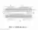
FIG. 1 is a schematic cross-sectional view of a conventional package stack structure 1. The package stack structure 1 has a lower packaging substrate 10, a semiconductor element 11 disposed in a flip-chip manner on the lower packaging substrate 10, an upper packaging substrate 12 bonded to and electrically coupled to the lower packaging substrate 10 through a plurality of supporting solder balls 13, at least an electronic device 16 such as a memory chip or a memory package structure disposed in a flip-chip manner on the upper packaging substrate 12, and an encapsulant 14 encapsulating the supporting solder balls 13 and the semiconductor element 11. Optionally, an underfill 19 is formed between the semiconductor element 11 and the lower packaging substrate 10.
The upper packaging substrate 12 is an organic packaging substrate, which can have a core layer 120 or be a coreless packaging substrate. Since the upper packaging substrate 12 generally has a thickness d of about 150 to 800 um, it becomes difficult to reduce the overall thickness D of the package stack structure 1 so as to meet the miniaturization requirement of electronic products.
Further, even if the upper packaging substrate 12 has a small thickness d, the height R of the supporting solder balls 13 must be greater than the height r of the semiconductor element 11 so as to prevent the semiconductor element 11 from impacting the upper packaging substrate 12 and causing damage. Therefore, limited by the height R of the supporting solder balls 13, the overall thickness D of the package stack structure 1 cannot be reduced to be less than 240 um.
Therefore, how to overcome the above-described drawbacks has become critical.
SUMMARY
In view of the above-described drawbacks, the present disclosure provides an electronic package, which comprises: a carrier; an electronic component disposed on the carrier, wherein the electronic component has a first side bonded to the carrier and a second side opposite to the first side; a plurality of conductors formed in the electronic component, communicating the first and second sides of the electronic component, and electrically connected to the carrier; an encapsulant formed on the carrier to encapsulate the electronic component; and an electronic device disposed on the encapsulant and electrically connected to the conductors, wherein the conductors are partially exposed from the encapsulant.
The present disclosure further provides a method for fabricating an electronic package, which comprises: disposing on a carrier at least an electronic component that has a first side bonded to the carrier and a second side opposite to the first side, wherein a plurality of conductors are formed in the electronic component, communicate the first and second sides of the electronic component, and are electrically connected to the carrier; forming an encapsulant on the carrier to encapsulate the electronic component in a manner that the conductors are partially exposed from the encapsulant, and disposing an electronic device on the encapsulant, wherein the electronic device is electrically connected to the conductors, the conductors are partially exposed from the encapsulant.
In an embodiment, a plurality of electrode pads are formed on the first or second side of the electronic component for the electronic component to be electrically connected to the carrier.
In an embodiment, the conductors protrude from the second side of the electronic component.
In an embodiment, an insulating material is formed between the electronic device and the encapsulant. In another embodiment, the insulating material is a dielectric material, a packaging material or a non-conductive film.
According to the present disclosure, the conductors are formed in the electronic component to electrically connect the carrier and the electronic device. Compared with the prior art, the present disclosure dispenses with the conventional upper packaging substrate and the supporting solder balls. Therefore, the material cost is saved, and the fabrication process is simplified. Further, the overall thickness of the electronic package is greatly reduced to meet the miniaturization requirement of electronic products.
BRIEF DESCRIPTION OF DRAWINGS
FIG. 1 is a schematic cross-sectional view of a conventional package stack structure;
FIGS. 2A to 2D are schematic cross-sectional views showing a method for fabricating an electronic package according to the present disclosure;
FIG. 2E is a schematic partial cross-sectional view showing another embodiment of FIG. 2D; and
FIGS. 3 and 4 are schematic cross-sectional views showing other embodiments of FIG. 2D.
DETAILED DESCRIPTION OF EMBODIMENTS
The following illustrative embodiments are provided to illustrate the disclosure of the present disclosure, these and other advantages and effects can be apparent to those in the art after reading this specification.
It should be noted that all the drawings are not intended to limit the present disclosure. Various modifications and variations can be made without departing from the spirit of the present disclosure. Further, terms such as “first”, “second”, “on”, “a” etc. are merely for illustrative purposes and should not be construed to limit the scope of the present disclosure.
FIGS. 2A to 2D are schematic cross-sectional views showing a method for fabricating an electronic package according to the present disclosure.
Referring to FIG. 2A, at least an electronic component 21 having a plurality of conductors 23 is disposed on a carrier 20.
In an embodiment, the carrier 20 is a packaging substrate having a core layer and a circuit structure, or a coreless circuit structure, and the carrier 20 has a plurality of circuit layers such as fan-out redistribution layers. Alternatively, the carrier 20 can be, for example, a lead frame.
The electronic component 21 is an active element, such as a semiconductor chip, a passive element, such as a resistor, a capacitor or an inductor, or a combination thereof. For example, the electronic component 21 is a semiconductor chip, which has a first side 21a (i.e., an active surface) with a plurality of electrode pads 210 and a second side 21b (i.e., an inactive surface) opposite to the first side 21a. The electrode pads 210 are disposed on and electrically connected to the carrier 20 through a plurality of conductive bumps 22. The conductive bumps 22 are made of a solder material, for example. In another embodiment, referring to FIG. 4, a plurality of electrode pads 410 are disposed on a second side 21b (i.e., an active surface) of an electronic component 41 and electrically connected to the carrier 20 through a plurality of bonding wires 42.
The conductors 23 are metal posts, such as copper posts, which are formed in the electronic component 21 by a TSV (through silicon via) process. Each of the conductors 23 has a first end portion 23a and a second end portion 23b opposite to the first end portion 23a. The first end portions 23a of the conductors 23 are exposed from the first side 21a of the electronic component 21 and electrically connected to the carrier 20 through a plurality of conductive bumps 22. The conductive bumps 22 are made of such as a solder material.
Further, an underfill 29 is optionally formed between the first side 21a of the electronic component 21 and the carrier 20 to encapsulate the conductive bumps 22.
Referring to FIG. 2B, an encapsulant 24 is formed on the carrier 20 to encapsulate the electronic component 21.
In an embodiment, the encapsulant 24 is formed by lamination or molding and made of a dielectric material or a packaging material, for example, polyimide, a dry film, an epoxy resin, or a molding compound.
The encapsulant 24 has a first surface 24a bonded to the carrier 20 and a second surface 24b opposite to the first surface 24a.
In another embodiment, referring to FIG. 3, an encapsulant 34 is optionally formed between the carrier 20 and the first side 21a of the electronic component 21 to encapsulate the conductive bumps 22.
In a further embodiment, referring to FIG. 4, the encapsulant 24 encapsulates the bonding wires 42.
Referring to FIG. 2C, a portion of the encapsulant 24 and the electronic component 21 is removed to expose the conductors 23. The conductors 23 communicate the first side 21a and the second side 21b of the electronic component 21.
In an embodiment, the second end portion 23b of the conductors 23 protrudes from the second side 21b of the electronic component 21. In an embodiment, a leveling process is performed to remove a portion of the electronic component 21 from the second side 21b thereof so as to cause the second end portions 23b of the conductors 23 to be flush with the second side 21b of the electronic component 21. Then, an etch process is performed to remove a portion of the electronic component 21 from the second side 21b thereof and hence the second end portion 23b of the conductors 23 protrudes from the second side 21b of the electronic component 21.
In an embodiment, a portion of the encapsulant 24, the conductors 23 and the electronic component 21 is removed by grinding or cutting so as to cause the second surface 24b of the encapsulant 24, the second end portions 23b of the conductors 23 and the second side 21b of the electronic component 21 to be coplanar. As such, the thickness T of the electronic component 21 (or the encapsulant 24 or the conductors 23) is less than 100 um. Then, a dry etch process such as a plasma etch process or a reactive ion etch process is performed to remove a portion of the electronic component 21 having a thickness t of about 10 um from the second side 21b thereof. Therefore, the second end portion 23b of the conductors 23 protrudes from the second side 21b of the electronic component 21.
Further, a plurality of solder balls 25 are formed on a lower surface of the carrier 20 so as for a circuit board to be mounted thereon.
Referring to FIG. 2D, an electronic device 26 is disposed on the second surface 24b of the encapsulant 24 and electrically connected to the conductors 23 through a plurality of conductive elements 260. As such, a PoP electronic package 2 is obtained.
In an embodiment, the electronic device 26 is a high bandwidth memory (HBM) package structure, and the conductive elements 260 are conductive bumps containing a solder material.
Further, after the electronic device 26 is disposed on the second surface 24b of the encapsulant 24, an insulating material 27 is formed to encapsulate and thus protect the conductive elements 260. Also, the insulating material 27 facilitates to enhance the rigidity of the electronic package 2. The insulating material 27 is made of a dielectric material or a packaging material.
In another embodiment, referring to FIG. 2E, an insulating material 28 is formed on the electronic device 26 to encapsulate the conductive elements 260. Thereafter, the electronic device 26 having the insulating material 28 is disposed on the second surface 24b of the encapsulant 24 and the conductive elements 260 are bonded and electrically connected to the conductors 23. As such, the insulating material 28 protects the conductive elements 260 and enhances the rigidity of the electronic package 2. The insulating material 28 can have a flux function and can be a non-conductive film such as an anisotropic conductive paste or an anisotropic conductive film.
According to the present disclosure, the conductors 23 are disposed in the electronic component 21, 41 to electrically connect the carrier 20 and the electronic device 26. Compared with the prior art, the present disclosure dispenses with the conventional upper packaging substrate and the supporting solder balls. Therefore, the material cost is saved and the fabrication process is simplified. Since the overall thickness H of the electronic package 2, 3, 4 mainly depends on the thickness h of the electronic component 21, 41 (or the thickness T of the conductors 23), the overall thickness H of the electronic package 2, 3, 4 can be greatly reduced to be less than 240 um, thus meeting the miniaturization requirement of electronic products.
The present disclosure further provides an electronic package 2, 3, 4, which has: a carrier 20; an electronic component 21, 41 disposed on the carrier 20, wherein the electronic component 21 has a first side 21a bonded to the carrier 20 and a second side 21b opposite to the first side 21a; a plurality of conductors 23 formed in the electronic component 21, 41, communicating the first and second sides 21a, 21b of the electronic component 21, and electrically connected to the carrier 20; an encapsulant 24, 34 formed on the carrier 20 to encapsulate the electronic component 21, 41, wherein the conductors 23 are partially exposed from the encapsulant 24, 34; and an electronic device 26 disposed on the encapsulant 24, 34 and electrically connected to the conductors 23.
In an embodiment, a plurality of electrode pads 210, 410 are disposed on the first side 21a or the second side 21b of the electronic component 21, 41 and electrically connected to the carrier 20.
In an embodiment, the conductors 23 protrude from the second side 21b of the electronic component 21, 41.
In an embodiment, an insulating material 27, 28 is formed between the electronic device 26 and the encapsulant 24, 34. In an embodiment, the insulating material 27, 28 is a dielectric material, a packaging material or a non-conductive film.
According to the present disclosure, the conductors are formed in the electronic component to electrically connect the carrier and the electronic device. Compared with the prior art, the present disclosure dispenses with the conventional upper packaging substrate and the supporting solder balls, and reduces the fabrication cost and the overall thickness of the electronic package.
The above-described descriptions of the detailed embodiments are only to illustrate the implementation according to the present disclosure, and it is not to limit the scope of the present disclosure. Accordingly, all modifications and variations completed by those with ordinary skill in the art should fall within the scope of present disclosure defined by the appended claims.
Claims
What is claimed is:1. An electronic package, comprising:
a carrier;
an electronic component disposed on the carrier and having a first side bonded to the carrier and a second side opposite to the first side;
a plurality of conductors formed in the electronic component, communicating the first and second sides of the electronic component, and electrically connected to the carrier;
an encapsulant formed on the carrier and encapsulating the electronic component, with the conductors being partially exposed from the encapsulant; and
an electronic device disposed on the encapsulant and electrically connected to the conductors.
2. The electronic package of claim 1, wherein the electronic component comprises a plurality of electrode pads disposed on the first or second side thereof for the electronic component to be electrically connected to the carrier.
3. The electronic package of claim 1, wherein the conductors protrude from the second side of the electronic component.
4. The electronic package of claim 1, further comprising an insulating material formed between the electronic device and the encapsulant.
5. The electronic package of claim 4, wherein the insulating material is a dielectric material, a packaging material or a non-conductive film.
6. A method for fabricating an electronic package, comprising:
disposing on a carrier at least an electronic component having a first side bonded to the carrier and a second side opposite to the first side, wherein a plurality of conductors are formed in the electronic component, communicate the first and second sides of the electronic component and are electrically connected to the carrier;
forming on the carrier an encapsulant for encapsulating the electronic component, with the conductors being partially exposed from the encapsulant; and
disposing on the encapsulant an electronic device electrically connected to the conductors.
7. The method of claim 6, wherein the electronic component has a plurality of electrode pads disposed on the first or second side thereof for the electronic component to be electrically connected to the carrier.
8. The method of claim 6, wherein the conductors protrude from the second side of the electronic component.
9. The method of claim 6, further comprising forming an insulating material between the electronic device and the encapsulant.
10. The method of claim 9, wherein the insulating material is a dielectric material, a packaging material or a non-conductive film.
Images & Drawings included:


Sources:
- United States Patent and Trademark Office - verify current appl. status at the USPTO↗
Similar patent applications:
- » 20220254869
Inductor structure having conductive sheets having fan plate shape arranged in ring structure and fabrication method thereof, electronic package and fabrication method thereof, and method for fabricating packaging carrier - » 20140203771
ELECTRONIC PACKAGE, FABRICATION METHOD THEREOF AND ADHESIVE COMPOUND - » 20160307833
ELECTRONIC PACKAGING STRUCTURE AND METHOD FOR FABRICATING ELECTRONIC PACKAGE - » 20180102469
Cryogenic electronic packages and methods for fabricating cryogenic electronic packages - » 20210057300
Electronic package, electronic packaging module having the electronic package, and method for fabricating the electronic package - » 20170194238
Substrate structure, electronic package and method for fabricating the electronic package - » 20160315044
Electronic device package, electronic device structure and method of fabricating electronic device package - » 13765388
Electronic component package fabrication method and structure - » 13327440
Electronic component package fabrication method and structure - » 13233606
Electronic component package fabrication method and structure
Recent applications in this class:
- » 20250293108 2025-09-18
SEMICONDUCTOR PACKAGE AND MANUFACTURING METHOD FOR THE SAME - » 20250285928 2025-09-11
SEMICONDUCTOR PACKAGE AND METHOD OF MANUFACTURING THE SAME - » 20250246493 2025-07-31
SEMICONDUCTOR DEVICE - » 20250239499 2025-07-24
ULTRA-THIN PACKAGED COMPONENT - » 20250233036 2025-07-17
INTEGRATED CIRCUIT WITH A PROTECTIVE LAYER - » 20250226276 2025-07-10
SEMICONDUCTOR DEVICE - » 20250210434 2025-06-26
SEMICONDUCTOR PACKAGE - » 20250210433 2025-06-26
PACKAGE STRUCTURE - » 20250167060 2025-05-22
THREE-DIMENSIONAL INTEGRATED CIRCUIT STRUCTURES AND METHODS OF FORMING THE SAME - » 20250140625 2025-05-01
SEMICONDUCTOR MODULE AND METHOD OF MANUFACTURING A SEMICONDUCTOR MODULE
Recent applications for this Assignee:
- » 20250046771 2025-02-06
METHOD FOR FABRICATING ELECTRONIC PACKAGE - » 20250015054 2025-01-09
CARRYING SUBSTRATE, ELECTRONIC PACKAGE HAVING THE CARRYING SUBSTRATE, AND METHODS FOR MANUFACTURING THE SAME - » 20240379534 2024-11-14
ELECTRONIC PACKAGE, MANUFACTURING METHOD FOR THE SAME, AND ELECTRONIC STRUCTURE - » 20240321798 2024-09-26
Electronic package and carrier thereof and method for manufacturing the same - » 20240321784 2024-09-26
Electronic package including lead frame having multiple conductive posts - » 20240321591 2024-09-26
METHOD FOR FABRICATING ELECTRONIC PACKAGE - » 20240290701 2024-08-29
ELECTRONIC PACKAGE AND MANUFACTURING METHOD THEREOF - » 20240290675 2024-08-29
Electronic package and manufacturing method thereof - » 20240290674 2024-08-29
ELECTRONIC PACKAGE AND MANUFACTURING METHOD THEREOF - » 20240282674 2024-08-22
ELECTRONIC PACKAGE AND METHOD OF FABRICATING THE SAME