Method for fabricating a structure for a microelectromechanical system (MEMS) device
US20050142684A1
2005-06-30
10/941,042
2004-09-14
✅ Patent granted
US 7,250,315 B2
2007-07-31
-
-
Savitri Mulpuri
2024-09-14
Abstract:
The invention provides a microfabrication process which may be used to manufacture a MEMS device. In one embodiment, the process comprises depositing at least one first layer on a substrate. The process further comprises patterning said first layer to define at least a first portion of said microelectromechanical system device. The process further comprises depositing a second layer on said first layer. The process further comprises patterning said second layer using said first layer as a photomask. The process further comprises developing said second layer to define at least a second portion of the microelectromechanical system device.
Assignee:
- IDC, LLC 160 🇺🇸 San Francisco, CA, United States
Interested in similar patents?
Get notified when new applications in this technology area are published.
Classification:
G02B26/001 » CPC main
Optical devices or arrangements for the control of light using movable or deformable optical elements based on interference in an adjustable optical cavity
B81C1/00396 » CPC further
Manufacture or treatment of devices or systems in or on a substrate; Etch mask forming Mask characterised by its composition, e.g. multilayer masks
B81B2201/042 » CPC further
Specific applications of microelectromechanical systems; Optical MEMS Micromirrors, not used as optical switches
B81B2203/0315 » CPC further
Basic microelectromechanical structures; Static structures Cavities
B81C2201/0109 » CPC further
Manufacture or treatment of microstructural devices or systems in or on a substrate; Shaping material; Structuring the bulk substrate or layers on the substrate; Film patterning; Surface micromachining; Sacrificial layer Sacrificial layers not provided for in -
B81C2203/0136 » CPC further
Forming microstructural systems; Packaging MEMS Growing or depositing of a covering layer
H01L21/00 IPC
Processes or apparatus adapted for the manufacture or treatment of semiconductor or solid state devices or of parts thereof
Description
FIELD OF THE INVENTIONThis invention relates to microfabrication. In particular, it relates to the microfabrication of a structure for a Microelectromechanical Systems (MEMS) device.
BACKGROUNDMicrofabrication techniques used to fabricate MEMS devices generally involve the deposition of one or more layers on a substrate and the subsequent patterning of the layers to produce useful structures. One technique for patterning a layer involves the use of photolithography. With photolithography a photographic definition of a desired pattern on a photo or optical mask is used to impart the pattern onto a surface of the layer. When manufacturing a MEMS device usually several masking steps are required, each masking step adding to the cost of the device. Accordingly, it is desirable to reduce the number of masking steps required during fabrication of a MEMS device.
SUMMARY OF THE INVENTIONAccording to one aspect of the invention there is provided a microfabrication process comprising depositing a first layer on a substrate; patterning the first layer; depositing a second layer on the first layer; and patterning the second layer using the first layer as a photomask.
BRIEF DESCRIPTION OF THE DRAWINGSFIG. 1 shows a three dimensional drawing of a part of a MEMS device which may be manufactured using the microfabrication process of the present invention; and
FIGS. 2 to 10 shows various stages in the manufacture of the MEMS device of FIG. 1.
DETAILED DESCRIPTIONAspects of the present invention will now be described with reference to FIGS. 2 to 10 of the drawings which show the stages during fabrication of a MEMS device such as a Visible Spectrum Modulator Array described in U.S. Pat. No. 5,835,255 or an Interferometric Modulater (IMOD) described in U.S. Pat. No. 6,040,937. Naturally, describing the present invention with reference to stages in the manufacture of a Visible Spectrum Modulator Array or an IMOD is intended to enhance understanding of the present invention and it is to be understood that the present invention may used in the manufacture of other MEMS devices. Thus, the description of the present invention with reference to the manufacture of a Visible Spectrum Modulator Array or an IMOD is intended to be non-limiting.
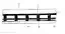
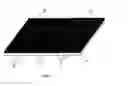
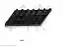
FIG. 1 of the drawings shows an example of a part of a Visible Spectrum Modulator Array 10 which may be fabricated in accordance with techniques described herein. Referring to FIG. 1, an antenna array is fabricated on one-half of a microfabricated interferometric cavity which transmits and reflects certain portions of incident electromagnetic radiation depending on (a) the dimensions of the cavity itself and (b) the frequency of response of dielectric mirrors in the cavities. In FIG. 1, the array 10 is shown to include two cavities 12, 14 fabricated on a transparent substrate 16. A layer 18, the primary mirror/conductor may comprise a combination of one or more films of metals, oxides, semiconductors, and transparent conductors. Insulating supports 20 hold up a second transparent conducting membrane 22. Each array element has an antenna array 24 formed on the membrane 22. The two structures 22, 24, together comprise the secondary mirror/conductor. Conversely, the antenna array may be fabricated as part of the primary mirror/conductor. Secondary, mirror/conductor 22/24 forms a flexible membrane, fabricated such that it is under tensile stress and thus parallel to the substrate, in an undriven state.
Because layers 22 and 24 are parallel, radiation which enters any of the cavities from above or below the array can undergo multiple reflections within the cavity, resulting in optical interference. Depending on the dimensions of the antenna array, the interference will determine its reflective and/or transmissive characteristics. Changing one of the dimensions, in this case the cavity height (i.e. the spacing between the inner walls of layers 18, 22), will alter the optical characteristics. The change in height is achieved by applying a voltage across the two layers of the cavity, which due to electrostatic forces, causes layer 22 to collapse. Cavity 12 is shown collapsed (7 volts applied), while cavity 14 is shown uncollapsed (0 volts applied).
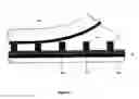
In fabricating the array 10, it is desirable that insulating supports 20 are well defined in regions where contact is made between insulating supports 20 and layers 18, 22. The present invention is especially useful in manufacturing such a support. FIGS. 2 through 10 show various stages in the manufacture of a MEMS device having supports such as the supports 20. Referring to FIG. 2 of the drawings, reference numeral 100 indicates a substrate 100. The substrate 100 may be of many different materials each being transparent to ultraviolet light. Examples of these materials include plastic, mylar, or quartz. The material must be able to support an optically smooth, though not necessarily flat, finish. A preferred material would likely be glass, which would be both transmissive and reflective operation in the visible range.
Various layers are deposited on substrate 100 to define a stack. In particular, the substrate 100 is coated with a sacrificial layer 102 using standard techniques such as a physical vapor deposition (PVD) method such as sputtering or e-beam evaporation. Other possible methods include chemical vapor deposition and molecular beam epitaxy.
In FIG. 2, the sacrificial layer is a single layer. However, in other embodiments of the invention layer 102 may be a stack of layers with an uppermost sacrificial layer.
FIG. 3 of the drawings shows a stage in the manufacture of the MEMS device wherein the sacrificial layer 102 has been patterned so as to define longitudinally spaced grooves 104. A standard procedure is used to pattern sacrificial layer 102 which includes exposing layer 102 through an appropriate mask and developing to produce the pattern.
In FIG. 4 of the drawings, a photosensitive polymeric material in the form of a negative-acting-photosensitive material which could be a negative photoresist has been spun onto sacrificial layer 102 with a thickness that is larger than the total height of the film stack defined by layers 100 and 102. Thereafter, the negative-acting-photosensitive material is exposed to ultraviolet light through substrate 100 and developed using conventional techniques. Because the longitudinal grooves 104 are the only means by which the negative-acting-photosensitive material is exposed, the negative-acting-photosensitive material over the stack is dissolved during a subsequent development process, leaving only longitudinal ridges 106 of negative-acting-photosensitive material disposed in grooves 104. Thus, it will be appreciated that by first patterning the sacrificial layer 102 and then exposing the negative-acting-photosensitive material through substrate 100 through longitudinal grooves 104 in the sacrificial layer 102, the sacrificial layer 102 acts as a photomask thereby allowing the negative-acting-photosensitive material to be lithographically patterned without the need for an additional masking step. In FIG. 5 of the drawings, a structural layer 108 has been deposited on the stack and the sacrificial layer 102 has been removed, thus the layer 108 is supported by ridges 106. It will be appreciated that by using different photomasks it will be possible to fabricate support structures of any desired geometry. Thus instead of ridges, in other embodiments pillars or posts may be formed. The layer 108 is highly conductive and reflective and will typically contain aluminum and nickel.
FIG. 6 of the drawings shows a subsequent stage in the manufacture of the MEMS device wherein the layer 108 is patterned into transversely extending strips. FIG. 7 of the drawings shows the film stack with an oxide spacer layer 110 deposited on layer 108. FIG. 8 of the drawings shows a stage in the manufacture of the MEMS device in which the oxide spacer layer 110 has been patterned. FIG. 9 of the drawings shows a stage in the manufacture of the MEMS device in which a sealing film 112 is being applied with a pressure adhesive 114 over the entire structure to protect the structure from damage due to mechanical shock loading and to prevent particulates from interfering with the operation of the IMOD structures. The sealing film 112 could be of a variety of materials such as thin metal films or polymeric films which have been coated with a metal or oxide film to provide hermeticity. Finally, FIG. 10 shows the structure after it has been purged with XeF2 gas to remove the remains of sacrificial layer 102. The edges of the structure are then sealed.
In other embodiments, instead of oxide layer 110 another layer of negative-acting-photosensitive material may be spun over oxide layer 110 and exposed through substrate 100 and using the techniques described above a further set of support structures may be formed. These support structures will provide support for other layers. It will be appreciated that the process may be repeated to build a MEMS structure having multiple layers or “floors” stacked one on top of the other wherein the floors are vertically spaced by support structures fabricated in accordance with the above techniques. One advantage of the present invention is that it provides a microfabrication technique which allows a mechanical support between two layers in an MEMS device to be precisely defined. This allows a clean, well-defined mechanical contact between the support and other structures within the MEMS device.
Further, the present invention uses a patterned layer on a substrate as a photomask to pattern another layer, thereby saving on a masking step.
Although the present invention has been described with reference to specific exemplary embodiments, it will be evident that the various modification and changes can be made to these embodiments without departing from the broader spirit of the invention as set forth in the claims. Accordingly, the specification and drawings are to be regarded in an illustrative sense rather than in a restrictive sense.
Claims
1. A method of fabricating a microelectromechanical system device, comprising:
depositing at least one first layer on a substrate;
patterning said first layer to define at least a first portion of said microelectromechanical system device;
depositing a second layer on said first layer;
patterning said second layer using said first layer as a photomask; and
developing said second layer to define at least a second portion of the microelectromechanical system device.
Images & Drawings included:

Sources:
- United States Patent and Trademark Office - verify current appl. status at the USPTO↗
Similar patent applications:
Recent applications in this class:
- » 20250284115 2025-09-11
Method for Treating an Optical Spacer - » 20250251585 2025-08-07
WAVELENGTH VARIABLE INTERFERENCE FILTER - » 20250208404 2025-06-26
OPTICAL PULSE STRETCHER APPARATUS - » 20240418981 2024-12-19
Optical Module, Electronic Device, And Driving Method - » 20240393578 2024-11-28
ANTI-PEEPING STRUCTURE AND ELECTRONIC DISPLAY DEVICE - » 20240369824 2024-11-07
MEMS Based Spatial Light Modulators and Applications - » 20240264426 2024-08-08
Full-color reversible switching device controlled by electrochemistry, and its preparation method and use - » 20240219708 2024-07-04
METHOD FOR MANUFACTURING MULTIPLE FILTERS WITH FABRY-PEROT CAVITY STRUCTURE, MULTISPECTRAL TRANSMISSION FILTER ARRAY AND MULTISPECTRAL TRANSMISSION FILTER STRUCTURE - » 20240176129 2024-05-30
OPTICAL FILTER FOR A MULTISPECTRAL SENSOR AND METHOD FOR MANUFACTURING SUCH A FILTER - » 20240142764 2024-05-02
GETTER VACUUM PUMP TO MAINTAIN VACUUM PRESSURE WITHIN A HOUSING OF A FABRY-PEROT CAVITY
Recent applications for this Assignee:
- » 20090267869 2009-10-29
Display device - » 20090225394 2009-09-10
System and method of illuminating interferometric modulators using backlighting - » 20090224748 2009-09-10
System and method of sensing actuation and release voltages of an interferometric modulator - » 20090219600 2009-09-03
Systems and methods of actuating MEMS display elements - » 20090213449 2009-08-27
MEMS display - » 20090201566 2009-08-13
Device having a conductive light absorbing mask and method for fabricating same - » 20090135466 2009-05-28
Method and device for multistate interferometric light modulation - » 20090135465 2009-05-28
System and method for multi-level brightness in interferometric modulation - » 20090122036 2009-05-14
Controller and driver features for bi-stable display - » 20090097100 2009-04-16
Optical films for controlling angular characteristics of displays