Semiconductor package system with substrate heat sink
US20060103010A1
2006-05-18
11/164,132
2005-11-10
✅ Patent granted
US 8,125,076 B2
2012-02-28
-
-
Chris Chu
2027-07-17
Abstract:
A semiconductor package system is provided including: providing a substrate having substrate wiring and a cavity provided therein with a heat sink foil closing off the cavity; attaching a semiconductor die in the cavity to the heat sink foil; and bonding the semiconductor die to the substrate wiring.
Inventors:
- Koo Hong Lee 19 🇰🇷 Seoul, South Korea
- Gwang Kim 2 🇸🇬 Singapore, Singapore
- Koo Hong Lee 2 🇸🇬 Singapore, Singapore
- Gwang Kim 4 🇰🇷 Kyoungki-do, South Korea
Assignee:
- STATS CHIPPAC, LTD. 1,631 🇸🇬 Singapore, Singapore
Interested in similar patents?
Get notified when new applications in this technology area are published.
Classification:
H01L2924/00014 » CPC further
Indexing scheme for arrangements or methods for connecting or disconnecting semiconductor or solid-state bodies as covered by; Technical content checked by a classifier the subject-matter covered by the group, the symbol of which is combined with the symbol of this group, being disclosed without further technical details
H01L2924/207 » CPC further
Indexing scheme for arrangements or methods for connecting or disconnecting semiconductor or solid-state bodies as covered by; Parameters Diameter ranges
H01L23/36 » CPC main
Details of semiconductor or other solid state devices; Arrangements for cooling, heating, ventilating or temperature compensation ; Temperature sensing arrangements Selection of materials, or shaping, to facilitate cooling or heating, e.g. heatsinks
H01L23/49816 » CPC further
Details of semiconductor or other solid state devices; Arrangements for conducting electric current to or from the solid state body in operation, e.g. leads, terminal arrangements ; Selection of materials therefor consisting of soldered constructions; Leads, on insulating substrates,; Additional leads joined to the metallisation on the insulating substrate, e.g. pins, bumps, wires, flat leads Spherical bumps on the substrate for external connection, e.g. ball grid arrays [BGA]
H01L25/105 » CPC further
Assemblies consisting of a plurality of individual semiconductor or other solid state devices ; Multistep manufacturing processes thereof all the devices being of a type provided for in the same subgroup of groups - , e.g. assemblies of rectifier diodes the devices having separate containers the devices being of a type provided for in group
H01L24/48 » CPC further
Arrangements for connecting or disconnecting semiconductor or solid-state bodies; Methods or apparatus related thereto; Means for bonding being attached to, or being formed on, the surface to be connected, e.g. chip-to-package, die-attach, "first-level" interconnects; Manufacturing methods related thereto; Wire connectors; Manufacturing methods related thereto; Structure, shape, material or disposition of the wire connectors after the connecting process of an individual wire connector
H01L24/73 » CPC further
Arrangements for connecting or disconnecting semiconductor or solid-state bodies; Methods or apparatus related thereto Means for bonding being of different types provided for in two or more of groups , , , , , , ,
H01L2225/1035 » CPC further
Details relating to assemblies covered by the group but not provided for in its subgroups; All the devices being of a type provided for in the same subgroup of groups - the devices having separate containers the devices being of a type provided for in group the containers being in a stacked arrangement the lowermost container comprising a device support the device being entirely enclosed by the support, e.g. high-density interconnect [HDI]
H01L2225/1058 » CPC further
Details relating to assemblies covered by the group but not provided for in its subgroups; All the devices being of a type provided for in the same subgroup of groups - the devices having separate containers the devices being of a type provided for in group the containers being in a stacked arrangement; Details of electrical connections between containers Bump or bump-like electrical connections, e.g. balls, pillars, posts
H01L2924/15311 » CPC further
Indexing scheme for arrangements or methods for connecting or disconnecting semiconductor or solid-state bodies as covered by; Details of package parts other than the semiconductor or other solid state devices to be connected; Die mounting substrate; Connection portion the connection portion being formed only on the surface of the substrate opposite to the die mounting surface being a ball array, e.g. BGA
H01L2924/1532 » CPC further
Indexing scheme for arrangements or methods for connecting or disconnecting semiconductor or solid-state bodies as covered by; Details of package parts other than the semiconductor or other solid state devices to be connected; Die mounting substrate; Connection portion the connection portion being formed on the die mounting surface of the substrate
H01L2924/15331 » CPC further
Indexing scheme for arrangements or methods for connecting or disconnecting semiconductor or solid-state bodies as covered by; Details of package parts other than the semiconductor or other solid state devices to be connected; Die mounting substrate; Connection portion the connection portion being formed on the die mounting surface of the substrate the connection portion being formed both on the die mounting surface of the substrate and outside the die mounting surface of the substrate being a ball array, e.g. BGA
H01L2924/3025 » CPC further
Indexing scheme for arrangements or methods for connecting or disconnecting semiconductor or solid-state bodies as covered by; Technical effects; Electrical effects Electromagnetic shielding
H01L2224/73265 » CPC further
Indexing scheme for arrangements for connecting or disconnecting semiconductor or solid-state bodies and methods related thereto as covered by; Means for bonding being of different types provided for in two or more of groups; Location after the connecting process on different surfaces Layer and wire connectors
H01L2924/14 » CPC further
Indexing scheme for arrangements or methods for connecting or disconnecting semiconductor or solid-state bodies as covered by; Details of semiconductor or other solid state devices to be connected; Device type Integrated circuits
H01L2924/00 » CPC further
Indexing scheme for arrangements or methods for connecting or disconnecting semiconductor or solid-state bodies as covered by
H01L2924/181 » CPC further
Indexing scheme for arrangements or methods for connecting or disconnecting semiconductor or solid-state bodies as covered by; Details of package parts other than the semiconductor or other solid state devices to be connected Encapsulation
H01L2924/00012 » CPC further
Indexing scheme for arrangements or methods for connecting or disconnecting semiconductor or solid-state bodies as covered by; Technical content checked by a classifier Relevant to the scope of the group, the symbol of which is combined with the symbol of this group
H01L2224/45099 » CPC further
Indexing scheme for arrangements for connecting or disconnecting semiconductor or solid-state bodies and methods related thereto as covered by; Means for bonding being attached to, or being formed on, the surface to be connected, e.g. chip-to-package, die-attach, "first-level" interconnects; Manufacturing methods related thereto; Wire connectors; Manufacturing methods related thereto; Structure, shape, material or disposition of the wire connectors prior to the connecting process of an individual wire connector; Core members of the connector Material
H01L23/34 IPC
Details of semiconductor or other solid state devices Arrangements for cooling, heating, ventilating or temperature compensation ; Temperature sensing arrangements
H01L23/10 IPC
Details of semiconductor or other solid state devices; Containers; Seals characterised by the material or arrangement of seals between parts, e.g. between cap and base of the container or between leads and walls of the container
Description
CROSS-REFERENCE TO RELATED APPLICATION(S)This application claims the benefit of U.S. Provisional Patent Application Ser. No. 60/627,645 filed Nov. 12, 2004 and the subject matter thereof is hereby incorporated herein by reference thereto.
TECHNICAL FIELDThe present invention relates generally to semiconductor package system, and more particularly to semiconductor package systems with heat sinks.
BACKGROUND ARTIn the electronics industry, a continuing objective is to further and further reduce the size of electronic devices while simultaneously increasing performance and speed. Cellular telephones, personal data devices, notebook computers, camcorders, and digital cameras are but a few of the consumer products that require and benefit from this ongoing miniaturization of sophisticated electronics.
Integrated circuit (“IC”) assemblies for such complex electronic systems typically have a large number of interconnected IC chips. The IC chips are usually made from a semiconductor material such as silicon or gallium arsenide. Photolithographic techniques are used to form the various semiconductor devices in multiple layers on the IC chips.
Heat management through such a structure can be critical. The internal thermal resistance and thermal performance of the flip chip interconnect technology are determined by a series of heat flow paths. By making high heat conductivity connections between the bottom of the die and the substrate, heat generated in the die can be transferred efficiently from the die to the substrate.
For applications where additional heat must be removed from the semiconductor die, the molding compound that encapsulates the die can be partially omitted from the upper surface of the die to partially expose this surface. The exposed die surface can then be put in direct physical contact with a heat spreader that overlies the semiconductor die. To enhance the cooling performance, a layer of thermal grease or the like can be spread between the die surface and the heat spreader to improve heat transfer to the heat spreader.
The heat spreader is typically formed so that it can also be attached to the underlying substrate, resulting in a mechanically strong package. Where necessary, the heat spreader can also be encapsulated in a molding compound that is formed overlying the upper surface of the package.
The heat thus flows first from the semiconductor device to the body of the semiconductor module or package into which it has been incorporated, and then to the package surface and to the heat spreader that is attached to the package surface. Unfortunately, there are drawbacks associated with the use of known heat spreaders and other semiconductor packages. Among these drawbacks are heat spreader manufacturing costs, complicated assembly processes, and concerns about package reliability.
Modern electronic systems demand continued decreases in size. The volumetric size of systems is dependent not only on the area of the semiconductor package, but also on the thickness of the semiconductor package. Using thin semiconductor packages allows smaller electronic systems to be built. Current trends place a premium on semiconductor packages that can incorporate multiple semiconductor dies in stacks or stacks of packages.
One proposed solution involves providing a heat sink or metal slug attached to the semiconductor package to help remove the heat. Unfortunately, this additional heat sink or metal slug adds to the package thickness, and prevents stacking of multiple packages.
Another proposed solution involves mounting the semiconductor die within an interior metal housing having sidewalls and flanges for retention. Unfortunately, this creates the need to use longer bond wires. Additionally, added vertical stress is created by the metal sidewalls of the housing.
Thus, a need still remains for thin packages with high thermal dissipation and it is increasingly critical that answers be found to these problems.
Solutions to these problems have been long sought but prior developments have not taught or suggested any solutions and, thus, solutions to these problems have long eluded those skilled in the art.
DISCLOSURE OF THE INVENTIONThe present invention provides a semiconductor package system including: providing a substrate having substrate wiring and a cavity provided therein with a heat sink foil closing off the cavity; attaching a semiconductor die in the cavity to the heat sink foil; and bonding the semiconductor die to the substrate wiring.
Certain embodiments of the invention have other aspects in addition to or in place of those mentioned above. The aspects will become apparent to those skilled in the art from a reading of the following detailed description when taken with reference to the accompanying drawings.
BRIEF DESCRIPTION OF THE DRAWINGSFIG. 1 is a cross sectional view of a semiconductor package system in an initial stage of manufacture in accordance with an embodiment of the present invention;
FIG. 2 is a cross sectional view of the structure of FIG. 1 in a die attach stage;
FIG. 3 is a cross sectional view of the structure of FIG. 2 in an encapsulation stage;
FIG. 4 is a cross sectional view of the structure of FIG. 3 in a flipped stage;
FIG. 5 is a cross sectional view of the structure of FIG. 4 in a board attach stage;
FIG. 6 is a cross sectional view of a semiconductor package system in accordance with another embodiment of the present invention; and
FIG. 7 is a flow chart of a semiconductor package system for manufacturing a semiconductor package system in accordance with a further embodiment of the present invention.
BEST MODE FOR CARRYING OUT THE INVENTIONThe following embodiments are described in sufficient detail to enable those skilled in the art to make and use the invention, and it is to be understood that other embodiments would be evident based on the present disclosure and that process or mechanical changes may be made without departing from the scope of the present invention.
In the following description, numerous specific details are given to provide a thorough understanding of the invention. However, it will be apparent that the invention may be practiced without these specific details. In order to avoid obscuring the present invention, some well-known process steps are not disclosed in detail.
Additionally, the drawings showing embodiments of the semiconductor package system are semi-diagrammatic and not to scale and, particularly, some of the dimensions are for the clarity of presentation and are shown exaggerated in the drawing FIGs.
The same number is used to designate similar parts as a matter of convenience and for ease of understanding the present invention.
The term “horizontal” as used herein is defined as a plane parallel to the plane or surface of the semiconductor die, regardless of its orientation. The term “vertical” refers to a direction perpendicular to the horizontal as just defined. Terms, such as “above”, “below”, “bottom”, “top”, “side” (as in “sidewall”), “higher”, “lower”, “upper”, “over”, and “under”, are defined with respect to the horizontal plane. The term “on” means that there is contact among different elements.
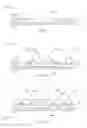
Referring now to FIG. 1, therein is shown a cross sectional view of a semiconductor package system 100 in an initial stage of manufacture in accordance with an embodiment of the present invention. The semiconductor package system 100 is a single system and includes a substrate 102 having a cavity 104. The cavity 104 is a through cavity and can be of any shape and in any location in the substrate 102. The substrate 102 includes a substrate core or prepreg material 106 with integral top and bottom foils 108 and 110 connected by vias 112. The bottom foil 110 closes off the bottom of the cavity 104.
The substrate 102 can be part of a long substrate strip 102 upon which a large number of semiconductor package systems 100 can be formed and later singulated but for purposes of simplicity only one semiconductor package system 100 is shown being formed.
By controlling the thickness or thinness of the substrate 102, the thickness or thinness semiconductor package system 100 can be affected directly.
Referring now to FIG. 2, a cross sectional view of the structure of FIG. 1 in a die attach stage. The top and bottom foils 108 and 110 are processed to form substrate wiring 200 and a conductive foil referred to as a heat sink foil 202.
Solder balls 204 are deposited on the substrate wiring 200 and a semiconductor die 206 is bonded to the heat sink foil 202 by a die attach adhesive 208. The semiconductor die 206 is then wire bonded to the substrate wiring 200 by bond wires 210. The semiconductor die 206 is electrically in contact with the solder balls 204.
Optionally, the semiconductor die 206 can be attached to the heat sink foil 202 by the die attach adhesive 208, which can be a solder or thermal grease, for better heat transfer than through an epoxy die attach adhesive.
Referring now to FIG. 3, therein is shown a cross sectional view of the structure of FIG. 2 in an encapsulation stage. An encapsulant 300 is molded over the heat sink foil 202, the die attach adhesive 208, the semiconductor die 206, and around the bond wires 210.
The heat sink foil 202 on the bottom is not covered by the encapsulant 300 so it provides a superior convention heat sink.
By controlling the thickness or thinness of the solder balls 204 and the encapsulant 300, the thickness or thinness semiconductor package system 100 can be affected directly.
Referring now to FIG. 4, therein is shown a cross sectional view of the structure of FIG. 3 in a flipped stage. The solder balls 204 extend further below the substrate 102 than the encapsulant 300.
Referring now to FIG. 5, therein is shown a cross sectional view of the structure of FIG. 4 in a board attach stage. Since the solder balls 204 extend further below the substrate 102 than the encapsulant 300, the solder balls 204 support the semiconductor package system 100 above a printed circuit board 500.
The heat sink foil 202 is exposed for direct heat transfer to the air above the die 206. Where the semiconductor die 206 is a conductive die attach adhesive 208, the heat sink foil 202 can also be electrically connected to the printed circuit board 500 so the semiconductor die 206 can be biased by connection to a ground or a power source to provide a shield against exterior noise sources or to provide a conductive drain connection for carrier or hole leakage from the semiconductor die 206 to the printed circuit board 500.
It has been discovered that a thinner semiconductor package system can be created using a single substrate with a heat sink foil. This is an improvement upon other systems that use separate heat sink elements.
Referring now to FIG. 6, therein is shown a cross sectional view of a semiconductor package system 600 in accordance with another embodiment of the present invention. The semiconductor package system 600 is a multiple-system system in which a number of semiconductor package systems 100 (three are shown by way of example) are stacked with the solder balls 204 of one semiconductor package system electrically connected with the substrate wiring 200 of the semiconductor package system below it.
Since the solder balls 204 extend further below the substrate 102 than the encapsulant 300, the heat sink foil 202 of each semiconductor package system 100 is exposed to permit heat transfer to the air.
In another option where a more rigid stack is desired, the entire semiconductor package system 600 can be encapsulated.
Referring now to FIG. 7, therein is shown a flow chart of a semiconductor package system 700 for manufacturing the semiconductor package system 100 in accordance with a further embodiment of the present invention. The system 700 includes: providing a substrate having substrate wiring and a cavity provided therein with a heat sink foil closing off the cavity; attaching a semiconductor die in the cavity to the heat sink foil; and bonding the semiconductor die to the substrate wiring.
It has been discovered that the present invention thus has numerous aspects. An aspect is that the present invention has reduced semiconductor package system height. Another aspect is improved thermal performance. Yet another theaspect of the present invention is that it valuably supports and services the historical trend of reducing costs, simplifying systems, and increasing performance.
These and other valuable aspects of the present invention consequently further the state-of-the-technology to at least the next level.
Thus, it has been discovered that the semiconductor package system of the present invention furnishes important and heretofore unknown and unavailable solutions, capabilities, and functional aspects for the semiconductor package system.
The resulting processes and configurations are straightforward, cost-effective, uncomplicated, highly versatile and effective, can be implemented by adapting known technologies, and are thus readily suited for efficiently and economically manufacturing semiconductor package systems.
The resulting processes and configurations are straightforward, cost-effective, uncomplicated, highly versatile, accurate, sensitive, and effective, and can be implemented by adapting known components for ready, efficient, and economical manufacturing, application, and utilization.
While the invention has been described in conjunction with a specific best mode, it is to be understood that many alternatives, modifications, and variations will be apparent to those skilled in the art in light of the aforegoing description. Accordingly, it is intended to embrace all such alternatives, modifications, and variations, which fall within the scope of the included claims. All matters hithertofore set forth herein or shown in the accompanying drawings are to be interpreted in an illustrative and non-limiting sense.
Claims
What is claimed is:1. A semiconductor package system comprising:
providing a substrate having substrate wiring and a cavity provided therein with a heat sink foil closing off the cavity;
attaching a semiconductor die in the cavity to the heat sink foil; and
bonding the semiconductor die to the substrate wiring.
2. The system as claimed in claim 1 wherein attaching the semiconductor die includes conductively connecting the semiconductor die to the heat sink foil.
3. The system as claimed in claim 1 wherein providing the substrate includes providing the substrate from a substrate strip for manufacturing a plurality of semiconductor package systems.
4. The system as claimed in claim 1 further comprising conductively connecting the semiconductor die to the heat sink foil to a printed circuit board.
5. The system as claimed in claim 1 further comprising:
mounting the substrate on a printed circuit board, the substrate having first substrate wiring; and
stacking a second substrate on the substrate, the second substrate having solder balls for conductive connection to the first substrate wiring.
6. A semiconductor package system comprising:
providing a substrate having substrate wiring and a cavity provided therein and a heat sink foil closing off the cavity;
attaching solder balls to the substrate wiring;
attaching a semiconductor die in the cavity to the heat sink foil;
wire bonding the semiconductor die to the substrate wiring; and
encapsulating the semiconductor die in the cavity.
7. The system as claimed in 6 wherein attaching the semiconductor die uses a conductive die attach adhesive to conductively connect the semiconductor die to the heat sink foil.
8. The system as claimed in 6 wherein:
providing the substrate includes providing the substrate from a substrate strip;
attaching a semiconductor die includes attaching a plurality of semiconductor die to the substrate strip; and
singulating the substrate strip into a plurality of substrates.
9. The system as claimed in 6 further comprising:
mounting the substrate on a printed circuit board using the solder balls; and
conductively connecting the semiconductor die and heat sink foil to the printed circuit board.
10. The system as claimed in 6 wherein:
encapsulating the semiconductor die forms a first semiconductor package system;
mounting the first semiconductor package system on a printed circuit board, the first semiconductor package system having first substrate wiring; and
stacking a second semiconductor package system on the first semiconductor package system, the second semiconductor package system having solder balls conductively connected to the first substrate wiring.
11. A semiconductor package system comprising:
a substrate having substrate wiring and a cavity provided therein with a heat sink foil closing off the cavity;
a semiconductor die in the cavity attached to the heat sink foil; and
electrical connections for the connection of the semiconductor die to the substrate wiring.
12. The system as claimed in claim 11 further comprising a conductive connection for connecting the semiconductor die to the heat sink foil.
13. The system as claimed in claim 11 wherein the substrate is part of a substrate strip for manufacturing a plurality of semiconductor package systems.
14. The system as claimed in claim 11 further comprising:
a printed circuit board; and
a conductive connection for connecting the semiconductor die to the heat sink foil to the printed circuit board.
15. The system as claimed in claim 11 further comprising:
the substrate mounted on a printed circuit board, the substrate having first substrate wiring; and
a second substrate stacked on the substrate, the second substrate having solder balls for conductive connection to the first substrate wiring.
16. The system as claimed in claim 11 further comprising:
solder balls on the substrate wiring;
bond wires connecting the semiconductor die to the substrate wiring; and
an encapsulant around the semiconductor die in the cavity.
17. The system as claimed in claim 16 further comprising a conductive die attach adhesive to conductively connect the semiconductor die to the heat sink foil.
18. The system as claimed in claim 16 wherein:
the substrate is part of a substrate strip; and
a plurality of semiconductor die are mounted to the substrate strip.
19. The system as claimed in claim 16 further comprising:
a printed circuit board;
the substrate mounted on the printed circuit board by the solder balls; and
the semiconductor die and the heat sink foil are conductively connected to the printed circuit board.
20. The system as claimed in claim 16 further comprising:
a printed circuit board;
the semiconductor die is included in a first semiconductor package system;
the first semiconductor package system is mounted on the printed circuit board, the first semiconductor package system having first substrate wiring; and
a second semiconductor package system stacked on the first semiconductor package system, the second semiconductor package system having solder balls conductively connected to the first substrate wiring.
Images & Drawings included:


Sources:
- United States Patent and Trademark Office - verify current appl. status at the USPTO↗
Recent applications in this class:
- » 20250293110 2025-09-18
SEMICONDUCTOR MODULE AND POWER CONVERSION UNIT - » 20250259906 2025-08-14
THERMAL PERFORMANCE IN HYBRID BONDED 3D DIE STACKS - » 20250226278 2025-07-10
SEMICONDUCTOR STRUCTURE AND MANUFACTURING METHOD THEREOF - » 20250226277 2025-07-10
SEMICONDUCTOR DEVICE AND MANUFACTURING METHOD THEREOF - » 20250210440 2025-06-26
SEMICONDUCTOR PACKAGE AND MANUFACTURING METHOD FOR THE SAME - » 20250201648 2025-06-19
INTEGRATED CIRCUIT PACKAGES - » 20250201647 2025-06-19
PACKAGE STRUCTURE - » 20250118615 2025-04-10
PACKAGE STRUCTURE INCLUDING A HEAT DISSIPATION STRUCTURE AND METHODS OF FORMING THE SAME - » 20250112105 2025-04-03
SEMICONDUCTOR ASSEMBLIES INCLUDING VERTICALLY INTEGRATED CIRCUITS AND METHODS OF MANUFACTURING THE SAME - » 20250105082 2025-03-27
PACKAGING STRUCTURE AND METHOD FOR FORMING THE SAME
Recent applications for this Assignee:
- » 20160351486 2016-12-01
Semiconductor device and method of forming substrate including embedded component with symmetrical structure - » 20160300817 2016-10-13
Semiconductor device and method of forming a package in-fan out package - » 20160300797 2016-10-13
Double-sided semiconductor package and dual-mold method of making same - » 20160276307 2016-09-22
Semiconductor device and method of forming PoP semiconductor device with RDL over top package - » 20160276238 2016-09-22
Semiconductor device and method of forming supporting layer over semiconductor die in thin fan-out wafer level chip scale package - » 20160233168 2016-08-11
Semiconductor device and method of forming 3D dual side die embedded build-up semiconductor package - » 20160218089 2016-07-28
Semiconductor device and method of forming WLCSP with semiconductor die embedded within interconnect structure - » 20160214857 2016-07-28
Semiconductor device and method of forming MEMS package - » 20160197059 2016-07-07
Semiconductor device and method of forming shielding layer over integrated passive device using conductive channels - » 20160197022 2016-07-07
Semiconductor device and method of forming sacrificial adhesive over contact pads of semiconductor die