Package structure of semiconductor and wafer-level formation thereof
US20060216859A1
2006-09-28
11/164,818
2005-12-07
✅ Patent granted
US 7,238,590 B2
2007-07-03
-
-
Theresa Doan | Sarah K. Harding
2026-01-06
Abstract:
In wafer-level formation of a package structure of semiconductor, multitudes of conductive connection structures are formed protruded from a transparent substrate. Multitudes of grooves are formed in a semiconductor wafer and an adhesive is filled therein. The wafer and the transparent substrate are jointed in which each of the conductive connection structures are positioned in one of the grooves and exposed outside of another surface of the semiconductor wafer. A package structure is obtained by sawing the wafer and has electrical connection between the signals of the active side and back side through the conductive connection structures.
Inventors:
- Kuo-Pin Yang 3 🇹🇼 Kao-Hsiung Hsien, Taiwan
- Wei-Min Hsiao 6 🇹🇼 Kao-Hsiung City, Taiwan
- Wei-Min Hsiao 5 🇹🇼 Kao-Hsiung, Taiwan
Assignee:
- Advanced Semiconductor Engineering, Inc. 18 🇹🇼 Kao-Hsiung, Taiwan
Interested in similar patents?
Get notified when new applications in this technology area are published.
Classification:
H01L27/14618 » CPC main
Devices consisting of a plurality of semiconductor or other solid-state components formed in or on a common substrate including semiconductor components sensitive to infra-red radiation, light, electromagnetic radiation of shorter wavelength or corpuscular radiation and specially adapted either for the conversion of the energy of such radiation into electrical energy or for the control of electrical energy by such radiation; Devices controlled by radiation; Imager structures; Structural or functional details thereof Containers
B81C1/0023 » CPC further
Manufacture or treatment of devices or systems in or on a substrate for manufacturing microsystems; Integrating an electronic processing unit with a micromechanical structure Packaging together an electronic processing unit die and a micromechanical structure die
H01L27/14632 » CPC further
Devices consisting of a plurality of semiconductor or other solid-state components formed in or on a common substrate including semiconductor components sensitive to infra-red radiation, light, electromagnetic radiation of shorter wavelength or corpuscular radiation and specially adapted either for the conversion of the energy of such radiation into electrical energy or for the control of electrical energy by such radiation; Devices controlled by radiation; Imager structures; Structural or functional details thereof Wafer-level processed structures
H01L27/14687 » CPC further
Devices consisting of a plurality of semiconductor or other solid-state components formed in or on a common substrate including semiconductor components sensitive to infra-red radiation, light, electromagnetic radiation of shorter wavelength or corpuscular radiation and specially adapted either for the conversion of the energy of such radiation into electrical energy or for the control of electrical energy by such radiation; Devices controlled by radiation; Imager structures; Processes or apparatus peculiar to the manufacture or treatment of these devices or parts thereof Wafer level processing
B81C2203/0118 » CPC further
Forming microstructural systems; Packaging MEMS Bonding a wafer on the substrate, i.e. where the cap consists of another wafer
H01L24/03 » CPC further
Arrangements for connecting or disconnecting semiconductor or solid-state bodies; Methods or apparatus related thereto; Means for bonding being attached to, or being formed on, the surface to be connected, e.g. chip-to-package, die-attach, "first-level" interconnects; Manufacturing methods related thereto; Bonding areas ; Manufacturing methods related thereto Manufacturing methods
H01L24/05 » CPC further
Arrangements for connecting or disconnecting semiconductor or solid-state bodies; Methods or apparatus related thereto; Means for bonding being attached to, or being formed on, the surface to be connected, e.g. chip-to-package, die-attach, "first-level" interconnects; Manufacturing methods related thereto; Bonding areas ; Manufacturing methods related thereto; Structure, shape, material or disposition of the bonding areas prior to the connecting process of an individual bonding area
H01L2224/0554 » CPC further
Indexing scheme for arrangements for connecting or disconnecting semiconductor or solid-state bodies and methods related thereto as covered by; Means for bonding being attached to, or being formed on, the surface to be connected, e.g. chip-to-package, die-attach, "first-level" interconnects; Manufacturing methods related thereto; Bonding areas; Manufacturing methods related thereto; Structure, shape, material or disposition of the bonding areas prior to the connecting process of an individual bonding area External layer
H01L2224/05573 » CPC further
Indexing scheme for arrangements for connecting or disconnecting semiconductor or solid-state bodies and methods related thereto as covered by; Means for bonding being attached to, or being formed on, the surface to be connected, e.g. chip-to-package, die-attach, "first-level" interconnects; Manufacturing methods related thereto; Bonding areas; Manufacturing methods related thereto; Structure, shape, material or disposition of the bonding areas prior to the connecting process of an individual bonding area; External layer Single external layer
H01L2224/81141 » CPC further
Indexing scheme for arrangements for connecting or disconnecting semiconductor or solid-state bodies and methods related thereto as covered by; Methods for connecting semiconductor or other solid state bodies using means for bonding being attached to, or being formed on, the surface to be connected using a bump connector; Aligning involving guiding structures, e.g. spacers or supporting members the guiding structures being at least partially left in the finished device Guiding structures both on and outside the body
H01L2224/81191 » CPC further
Indexing scheme for arrangements for connecting or disconnecting semiconductor or solid-state bodies and methods related thereto as covered by; Methods for connecting semiconductor or other solid state bodies using means for bonding being attached to, or being formed on, the surface to be connected using a bump connector; Arrangement of the bump connectors prior to mounting wherein the bump connectors are disposed only on the semiconductor or solid-state body
H01L2224/9202 » CPC further
Indexing scheme for arrangements for connecting or disconnecting semiconductor or solid-state bodies and methods related thereto as covered by; Methods for connecting semiconductor or solid state bodies including different methods provided for in two or more of groups - ; Specific sequence of method steps Forming additional connectors after the connecting process
H01L2924/1461 » CPC further
Indexing scheme for arrangements or methods for connecting or disconnecting semiconductor or solid-state bodies as covered by; Details of semiconductor or other solid state devices to be connected; Mixed devices MEMS
H01L2224/05599 » CPC further
Indexing scheme for arrangements for connecting or disconnecting semiconductor or solid-state bodies and methods related thereto as covered by; Means for bonding being attached to, or being formed on, the surface to be connected, e.g. chip-to-package, die-attach, "first-level" interconnects; Manufacturing methods related thereto; Bonding areas; Manufacturing methods related thereto; Structure, shape, material or disposition of the bonding areas prior to the connecting process of an individual bonding area; External layer Material
H01L2224/0555 » CPC further
Indexing scheme for arrangements for connecting or disconnecting semiconductor or solid-state bodies and methods related thereto as covered by; Means for bonding being attached to, or being formed on, the surface to be connected, e.g. chip-to-package, die-attach, "first-level" interconnects; Manufacturing methods related thereto; Bonding areas; Manufacturing methods related thereto; Structure, shape, material or disposition of the bonding areas prior to the connecting process of an individual bonding area; External layer Shape
H01L2924/00014 » CPC further
Indexing scheme for arrangements or methods for connecting or disconnecting semiconductor or solid-state bodies as covered by; Technical content checked by a classifier the subject-matter covered by the group, the symbol of which is combined with the symbol of this group, being disclosed without further technical details
H01L2224/0556 » CPC further
Indexing scheme for arrangements for connecting or disconnecting semiconductor or solid-state bodies and methods related thereto as covered by; Means for bonding being attached to, or being formed on, the surface to be connected, e.g. chip-to-package, die-attach, "first-level" interconnects; Manufacturing methods related thereto; Bonding areas; Manufacturing methods related thereto; Structure, shape, material or disposition of the bonding areas prior to the connecting process of an individual bonding area; External layer Disposition
H01L21/00 IPC
Processes or apparatus adapted for the manufacture or treatment of semiconductor or solid state devices or of parts thereof
H01L21/44 IPC
Processes or apparatus adapted for the manufacture or treatment of semiconductor or solid state devices or of parts thereof; Manufacture or treatment of semiconductor devices or of parts thereof the devices having at least one potential-jump barrier or surface barrier, e.g. PN junction, depletion layer or carrier concentration layer the devices having semiconductor bodies not provided for in groups, , , and with or without impurities, e.g. doping materials Manufacture of electrodes on semiconductor bodies using processes or apparatus not provided for in groups -
H01L21/48 IPC
Processes or apparatus adapted for the manufacture or treatment of semiconductor or solid state devices or of parts thereof; Manufacture or treatment of semiconductor devices or of parts thereof the devices having at least one potential-jump barrier or surface barrier, e.g. PN junction, depletion layer or carrier concentration layer Manufacture or treatment of parts, e.g. containers, prior to assembly of the devices, using processes not provided for in a single one of the subgroups -
H01L21/50 IPC
Processes or apparatus adapted for the manufacture or treatment of semiconductor or solid state devices or of parts thereof; Manufacture or treatment of semiconductor devices or of parts thereof the devices having at least one potential-jump barrier or surface barrier, e.g. PN junction, depletion layer or carrier concentration layer Assembly of semiconductor devices using processes or apparatus not provided for in a single one of the subgroups - , e.g. sealing of a cap to a base of a container
Description
BACKGROUND OF THE INVENTION1. Field of the Invention
The invention relates to a package structure and wafer-level fabrication thereof, and more particularly, to a package structure of integrating micro-electromechanical systems and image chips and wafer-level fabrication thereof.
2. Description of the Prior Art
The development of semiconductor processes has stimulated the progression of image sensor devices, such as complementary metal-oxide semiconductor (CMOS) sensors. In contrast to charged coupled device (CCD) sensors, CMOS sensors have the advantage of small size and cheap price even after being processed through the packaging process. However, ways to significantly increase the variability of designs and application of the CMOS sensors while maintaining the basic architecture has become a critical task. Additionally, ways to decrease the fabrication cost of the CMOS sensor package and apply the sensors to lower priced products has become another important factor.
Currently, the integration of micro-electromechanical systems (MEMS) and CMOS sensors into a package device has become an important technique in miniaturized packages, in which the operating space for micro-electromechanical systems has to be taken into great consideration. Hence, ways to lower the cost of fabricating an integrated package structure has become a critical matter.
SUMMARY OF THE INVENTIONIt is therefore an objective of the present invention to provide a package structure and wafer-level process for fabricating the same, in which a conductive structure formed on a substrate is utilized to penetrate another wafer, such that the electrical signals from one surface of the wafer can be transmitted to another surface of the wafer, thereby increasing the packaging flexibility of the micro-electromechanical devices and the image sensors.
It is another aspect of the present invention to provide a package structure of integrated chips and wafer-level process for fabricating the same, in which the package structure fabricated by penetrating a wafer is formed to reduce the complexity of the fabrication process and increase the overall yield.
Preferably, the package structure includes a semiconductor device having an active surface and a back surface, in which the active surface of the semiconductor device faces a substrate; a plurality of conductive connection structures disposed between the substrate and the semiconductor device and on the edge of the semiconductor device; a compliant layer on the back surface that exposes each conductive connection structure; a circuit layer on the compliant layer that contacts each conductive connection structure; and an insulating layer on the circuit layer that exposes part of the circuit layer.
These and other objectives of the present invention will no doubt become obvious to those of ordinary skill in the art after reading the following detailed description of the preferred embodiment that is illustrated in the various figures and drawings.
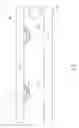
BRIEF DESCRIPTION OF THE DRAWINGSFIG. 1 is a cross-section diagram of a transparent substrate and a semiconductor wafer according to an embodiment of the present invention.
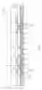
FIG. 2 is a cross-section diagram showing the processing of the semiconductor wafer according to an embodiment of the present invention.
FIG. 3 is a cross-section diagram showing the joining of the transparent substrate and the semiconductor wafer according to an embodiment of the present invention.
FIG. 4 is a cross-section diagram showing a means of joining and thinning the transparent substrate and the semiconductor wafer according to an embodiment of the present invention.
FIG. 5 is a cross-section diagram showing a means of joining the transparent substrate and the semiconductor wafer and fabricating a redistribution layer according to an embodiment of the present invention.
FIG. 6 is a cross-section diagram showing a means of joining the transparent substrate and the semiconductor wafer and fabricating solder balls and performing die singulation according to an embodiment of the present invention.
DETAILED DESCRIPTIONPlease refer to FIG. 1. FIG. 1 is a cross-section diagram of a transparent substrate and a semiconductor wafer according to an embodiment of the present invention. As shown in FIG. 1, a substrate 10 is provided, in which the substrate 10 includes a transparent substrate 101, such as a glass substrate, and a plurality of conductive connection structures formed on the transparent substrate 101. Preferably, a dry etching process is first preformed to form a plurality of grooves (not shown) on the transparent substrate 101, and a plurality of center structures 102 is formed thereafter by forming numerous protrusions by benzocyclobutene (BCB) on the transparent substrate 101. Subsequently, an electroplating process is performed to form a conductive layer 103 on the center structures 102 for forming the trace of the conductive connection structure.
Additionally, a wafer 20 includes a semiconductor substrate 201, a plurality of grooves 202 formed on an active surface 201a of the semiconductor substrate 201, and a back surface 201b on the corresponding opposite side of the active surface 201a. Preferably, the semiconductor substrate 201 is a substrate having optical chips or micro-electromechanical chips, and the grooves 202 are fabricated on the wafer scribe lines of the active surface 201 by utilizing conventional methods. Moreover, each groove 202 is located corresponding to each of the conductive connection structures, such that each conductive connection structure is positioned on the wafer scribe lines.
Please refer to FIG. 2. FIG. 2 is a cross-section diagram showing the processing of the semiconductor wafer according to an embodiment of the present invention. As shown in FIG. 2, an adhesive 203 is disposed in each of the grooves 202 for attaching each conductive connection structure of the substrate 10 in a later process. Preferably, the adhesive 203 is composed of a common adhesive material, such as epoxy, in which the quantity of the adhesive 203 may vary but is controlled at the amount that will not overflow to the active surface 201a in the later process. Next, an electroplating process is performed to form a plurality of bumps 204 on the area surrounding the grooves 202, in which the bumps 204 are utilized to adjust the joining and facilitate the electrical connection of the transparent substrate and the wafer in the later process. Preferably, the bumps 204 can be formed in the same process as the formation of the conductive layer 103, in which the depth of the conductive layer 103 can be utilized to adjust the joining and facilitate the electrical connection between the transparent substrate and the wafer thereafter.
Please refer to FIG. 3. FIG. 3 is a cross-section diagram showing the joining of the transparent substrate and the semiconductor wafer according to an embodiment of the present invention. As shown in FIG. 3, the conductive connection structures of the substrate 10 are disposed in the grooves 202 of the active surface 201a of the wafer 20 and into the adhesive 203, in which the surrounding area of the conductive layer 103 contacts the bumps 204. Preferably, the distance between the two wafers is adjusted by the depth of the conductive layer 103 and/or the height of the bumps 204 during the bonding of the substrate 10 and the wafer 20.
Please refer to FIG. 4. FIG. 4 is a cross-section diagram showing the means of joining and thinning the transparent substrate and the semiconductor wafer according to an embodiment of the present invention, in which part of the wafer 20 is removed from the back surface 201b for thinning the wafer 20. As shown in FIG. 4, a common planarizing process is performed to thin the wafer 20 that exposes one side of the conductive layer 103 from the thinned back surface 201c. A dry etching process is performed to remove the back surface 201c after the thinning process to form a slight protrusion of the conductive layer 103 from the back surface 201c. By utilizing the conductive connection structures of the substrate 10, the present invention is able to transmit the electrical signals from the conductive trace or the active surface 201a of the wafer 20 to the back surface 201c, and further establish a connection to the redistribution layer and the solder balls in the later process.
Please refer to FIG. 5. FIG. 5 is a cross-section diagram showing the means of joining the transparent substrate and the semiconductor wafer and fabricating a redistribution layer according to an embodiment of the present invention. As shown in FIG. 5, a compliant layer 205 is first formed on the back surface 201c, and a lithography process is performed to utilize a photoresist to remove a portion of the compliant layer 205 and expose the surface of the conductive layer 103. Next, a conductive layer is formed on the compliant layer 205 and contacting the exposed conductive layer 103, and another photoresist is formed to remove part of the conductive layer and form the circuit layer 206 containing the conductive pads. Preferably, the compliant layer 205, such as a benzocyclobutene (BCB) layer, is utilized to release the stress whereas the circuit layer 206 formed by a sputtering or an electroplating process, is electrically connected to the conductive layer 103 and functioning as the redistribution circuit layer.
Please refer to FIG. 6. FIG. 6 is a cross-section diagram showing the means of joining the transparent substrate and the semiconductor wafer and fabricating the solder balls and performing die singulation according to an embodiment of the present invention. As shown in FIG. 6, a coating process is performed to form an insulating layer 207, such as a solder mask on the circuit layer 206 and a lithography process is performed to remove part of the insulating layer 207 for exposing the conductive pads. Next, a solder ball mounting process is performed to dispose a plurality of solder balls 208 on the exposed surface of the conductive pads, in which the solder balls 208 are composed of tin-lead or non-lead materials. Despite the fact that only a circuit layer 206 is shown in the figure for fabricating the redistribution layer, the present invention is able to apply to the fabrication of multiple redistribution layers according to different product designs. Subsequently, a die singulation process is performed to dice the wafer along the scribe center lines 5. Preferably, the conductive layer 103 is positioned corresponding to the scribe center lines 5 and electrically connected to the solder balls 208 by utilizing the circuit layer 206. After the wafer is diced, the signals from the active surface 201a of the dies on the two adjacent side of the scribe center line 5 can be connected to the back surface 201c and further to the solder balls 208 through the conductive layer 103, thereby increasing the design flexibility of the device.
Consequently, the present invention provides a package structure for semiconductors and a wafer-level process for fabricating the same. Preferably, the package structure includes a semiconductor device having an active surface and a back surface, in which the active surface of the semiconductor device faces a substrate; a plurality of conductive connection structures disposed between the substrate and the semiconductor device and on the edge of the semiconductor device; a compliant layer on the back surface and exposes each conductive connection structure; a circuit layer on the compliant layer and contacts each conductive connection structure; and an insulating layer on the circuit layer and exposes part of the circuit layer.
Those skilled in the art will readily observe that numerous modifications and alterations of the device and method may be made while retaining the teachings of the invention. Accordingly, the above disclosure should be construed as limited only by the metes and bounds of the appended claims.
Claims
What is claimed is:1. A wafer-level package process comprising:
providing a substrate, wherein the substrate comprises a plurality of conductive connection structures protruding from the substrate;
providing a wafer having an active surface and a back surface, wherein the active surface comprises a plurality of grooves thereon;
forming an adhesive in each of the grooves;
joining the substrate and the wafer, wherein each conductive connection structure is positioned in each groove and the adhesive;
removing part of the wafer from the back surface for exposing each of the conductive connection structures;
forming a compliant layer on the back surface and exposing each of the exposed conductive connection structures;
forming at least a circuit layer on the compliant layer, wherein the circuit layer contacts the exposed conductive connection structures; and
forming an insulating layer on the circuit layer and exposing part of the circuit layer.
2. The wafer-level package process of claim 1 further comprising forming a plurality of solder balls on the exposed circuit layer.
3. The wafer-level package process of claim 1, wherein the step of providing the substrate comprises:
providing a transparent substrate;
forming a plurality of adhesive structures on the transparent substrate; and
electroplating a conductive layer on each adhesive structure for forming a conductive connection structure.
4. The wafer-level package process of claim 1, wherein the step of providing the wafer comprises utilizing an etching process for forming the plurality of grooves.
5. The wafer-level package process of claim 1, wherein the step of providing the wafer comprises electroplating a plurality of bumps on the active surface.
6. The wafer-level package process of claim 5, wherein the step of joining the substrate and the wafer further comprises utilizing the bumps for contacting the conductive connection structures.
7. The wafer-level package process of claim 1, wherein the step of removing part of the wafer comprises:
utilizing a chemical mechanical polishing (CMP) process for planarizing the wafer from the back surface; and
performing a micro-etching process on the planarized back surface.
8. The wafer-level package process of claim 1, wherein the step of forming the insulating layer comprises:
coating a solder resist on the circuit layer;
performing a lithography process on the solder resist; and
removing part of the solder resist for exposing part of the circuit layer.
9. The wafer-level package process of claim 1, wherein the step of forming the adhesive is achieved by utilizing a printing process.
10. A package structure of semiconductor comprising:
a substrate;
a semiconductor device having an active surface and a back surface, wherein the active surface of the semiconductor device faces the substrate;
a plurality of conductive connection structures disposed between the substrate and the semiconductor device and on the edge of the semiconductor device;
a compliant layer on the back surface that exposes each conductive connection structure;
a circuit layer on the compliant layer that contacts each conductive connection structure; and
an insulating layer on the circuit layer that exposes part of the circuit layer.
11. The package structure of semiconductor of claim 10 further comprising a plurality of solder balls connected to the exposed circuit layer.
12. The package structure of semiconductor of claim 10 further comprising an adhesive structure for attaching the conductive connection structures on the edge of the semiconductor device.
13. The package structure of semiconductor of claim 10, wherein the substrate is a glass substrate.
14. The package structure of semiconductor of claim 10, wherein the insulating layer comprises a solder resist.
Images & Drawings included:


Sources:
- United States Patent and Trademark Office - verify current appl. status at the USPTO↗
Recent applications in this class:
- » 20250048762 2025-02-06
SEMICONDUCTOR DEVICE, ELECTRONIC APPARATUS, AND MANUFACTURING METHOD OF SEMICONDUCTOR DEVICE - » 20250048761 2025-02-06
SEMICONDUCTOR PACKAGE STRUCTURE AND METHOD FOR PRODUCING THE SAME - » 20250048760 2025-02-06
ELECTRONIC DEVICE - » 20250040276 2025-01-30
IMAGE SENSOR PACKAGE - » 20250040275 2025-01-30
SENSOR PACKAGE STRUCTURE AND SENSING MODULE THEREOF - » 20250031468 2025-01-23
METHOD OF MANUFACTURING CONNECTION STRUCTURE, CONNECTION STRUCTURE, FILM STRUCTURE, AND METHOD OF MANUFACTURING FILM STRUCTURE - » 20250015105 2025-01-09
SUBSTRATE LAMINATE, IMAGE SENSOR, AND METHOD FOR MANUFACTURING SUSTRATE LAMINATE - » 20250006756 2025-01-02
IMAGE SENSING MODULE MANUFACTURING METHOD - » 20250006755 2025-01-02
SEMICONDUCTOR DEVICE AND ELECTRONIC EQUIPMENT - » 20240429253 2024-12-26
SEMICONDUCTOR APPARATUS AND ELECTRONIC DEVICE
Recent applications for this Assignee:
- » 20080220566 2008-09-11
Substrate process for an embedded component - » 20080164545 2008-07-10
MEMS microphone package and method thereof - » 20080157238 2008-07-03
MEMS microphone module and method thereof - » 20080087987 2008-04-17
Semiconductor packaging structure having electromagnetic shielding function and method for manufacturing the same - » 20080001308 2008-01-03
Flip-chip package structure with stiffener - » 20070291458 2007-12-20
Stacked semiconductor package having flexible circuit board therein - » 20070200239 2007-08-30
Redistribution connecting structure of solder balls - » 20070138615 2007-06-21
Packaging method of a plurality of chips stacked on each other and package structure thereof - » 20070132093 2007-06-14
System-in-package structure - » 20070087548 2007-04-19
Method for forming bumps