System-in-package structure
US20070132093A1
2007-06-14
11/420,230
2006-05-25
✅ Patent granted
US 7,417,329 B2
2008-08-26
-
-
S. V Clark
2026-10-11
Abstract:
A system-in-package structure includes a carrier substrate having a molding area and a periphery area, at least a chip disposed in the molding area, an encapsulation covering the chip and the molding area, a plurality of solder pads disposed in the periphery area, and a solder mask disposed in the periphery area and partially exposing the surface of the solder pads. The solder mask includes at least a void therein.
Inventors:
- Chi-Chih CHU 5 🇹🇼 Kao-Hsiung City, Taiwan
- Cheng-Yin LEE 5 🇹🇼 Tai-Nan City, Taiwan
- Meng-Jung Chuang 1 🇹🇼 Kao-Hsiung City, Taiwan
- Wei-Chang Tai 1 🇹🇼 Kao-Hsiung City, Taiwan
- Meng-Jung Chuang 1 🇹🇼 Kao-Hsiung, Taiwan
- Cheng-Yin Lee 2 🇹🇼 Tai-Nan, Taiwan
- Wei-Chang Tai 1 🇹🇼 Kao-Hsiung, Taiwan
- Chi-Chih Chu 2 🇹🇼 Kao-Hsiung, Taiwan
Assignee:
- Advanced Semiconductor Engineering, Inc. 18 🇹🇼 Kao-Hsiung, Taiwan
Interested in similar patents?
Get notified when new applications in this technology area are published.
Classification:
H01L2224/73265 » CPC further
Indexing scheme for arrangements for connecting or disconnecting semiconductor or solid-state bodies and methods related thereto as covered by; Means for bonding being of different types provided for in two or more of groups; Location after the connecting process on different surfaces Layer and wire connectors
H01L2924/10253 » CPC further
Indexing scheme for arrangements or methods for connecting or disconnecting semiconductor or solid-state bodies as covered by; Details of semiconductor or other solid state devices to be connected; Material of the semiconductor or solid state bodies; Semiconducting materials; Elemental semiconductors, i.e. Group IV Silicon [Si]
H01L2924/00014 » CPC further
Indexing scheme for arrangements or methods for connecting or disconnecting semiconductor or solid-state bodies as covered by; Technical content checked by a classifier the subject-matter covered by the group, the symbol of which is combined with the symbol of this group, being disclosed without further technical details
H01L25/105 » CPC main
Assemblies consisting of a plurality of individual semiconductor or other solid state devices ; Multistep manufacturing processes thereof all the devices being of a type provided for in the same subgroup of groups - , e.g. assemblies of rectifier diodes the devices having separate containers the devices being of a type provided for in group
H01L23/3128 » CPC further
Details of semiconductor or other solid state devices; Encapsulations, e.g. encapsulating layers, coatings, e.g. for protection characterised by the arrangement or shape the device being completely enclosed a substrate forming part of the encapsulation the substrate having spherical bumps for external connection
H05K3/3452 » CPC further
Apparatus or processes for manufacturing printed circuits; Assembling printed circuits with electric components, e.g. with resistor electrically connecting electric components or wires to printed circuits by soldering Solder masks
H05K3/3452 » CPC further
Apparatus or processes for manufacturing printed circuits; Assembling printed circuits with electric components, e.g. with resistor electrically connecting electric components or wires to printed circuits by soldering Solder masks
H01L23/49811 » CPC further
Details of semiconductor or other solid state devices; Arrangements for conducting electric current to or from the solid state body in operation, e.g. leads, terminal arrangements ; Selection of materials therefor consisting of soldered constructions; Leads, on insulating substrates, Additional leads joined to the metallisation on the insulating substrate, e.g. pins, bumps, wires, flat leads
H01L24/48 » CPC further
Arrangements for connecting or disconnecting semiconductor or solid-state bodies; Methods or apparatus related thereto; Means for bonding being attached to, or being formed on, the surface to be connected, e.g. chip-to-package, die-attach, "first-level" interconnects; Manufacturing methods related thereto; Wire connectors; Manufacturing methods related thereto; Structure, shape, material or disposition of the wire connectors after the connecting process of an individual wire connector
H01L24/73 » CPC further
Arrangements for connecting or disconnecting semiconductor or solid-state bodies; Methods or apparatus related thereto Means for bonding being of different types provided for in two or more of groups , , , , , , ,
H01L2224/05573 » CPC further
Indexing scheme for arrangements for connecting or disconnecting semiconductor or solid-state bodies and methods related thereto as covered by; Means for bonding being attached to, or being formed on, the surface to be connected, e.g. chip-to-package, die-attach, "first-level" interconnects; Manufacturing methods related thereto; Bonding areas; Manufacturing methods related thereto; Structure, shape, material or disposition of the bonding areas prior to the connecting process of an individual bonding area; External layer Single external layer
H01L2225/1023 » CPC further
Details relating to assemblies covered by the group but not provided for in its subgroups; All the devices being of a type provided for in the same subgroup of groups - the devices having separate containers the devices being of a type provided for in group the containers being in a stacked arrangement the lowermost container comprising a device support the support being an insulating substrate
H01L2225/1058 » CPC further
Details relating to assemblies covered by the group but not provided for in its subgroups; All the devices being of a type provided for in the same subgroup of groups - the devices having separate containers the devices being of a type provided for in group the containers being in a stacked arrangement; Details of electrical connections between containers Bump or bump-like electrical connections, e.g. balls, pillars, posts
H01L2225/107 » CPC further
Details relating to assemblies covered by the group but not provided for in its subgroups; All the devices being of a type provided for in the same subgroup of groups - the devices having separate containers the devices being of a type provided for in group the containers being in a stacked arrangement; Details of electrical connections between containers Indirect electrical connections, e.g. via an interposer, a flexible substrate, using TAB
H01L2924/15331 » CPC further
Indexing scheme for arrangements or methods for connecting or disconnecting semiconductor or solid-state bodies as covered by; Details of package parts other than the semiconductor or other solid state devices to be connected; Die mounting substrate; Connection portion the connection portion being formed on the die mounting surface of the substrate the connection portion being formed both on the die mounting surface of the substrate and outside the die mounting surface of the substrate being a ball array, e.g. BGA
H05K3/284 » CPC further
Apparatus or processes for manufacturing printed circuits; Secondary treatment of printed circuits; Applying non-metallic protective coatings for encapsulating mounted components
H05K3/284 » CPC further
Apparatus or processes for manufacturing printed circuits; Secondary treatment of printed circuits; Applying non-metallic protective coatings for encapsulating mounted components
H05K2203/0588 » CPC further
Indexing scheme relating to apparatus or processes for manufacturing printed circuits covered by; Patterning and lithography; Masks; Details of resist; Details of resist Second resist used as pattern over first resist
H05K2203/0588 » CPC further
Indexing scheme relating to apparatus or processes for manufacturing printed circuits covered by; Patterning and lithography; Masks; Details of resist; Details of resist Second resist used as pattern over first resist
H01L2924/15311 » CPC further
Indexing scheme for arrangements or methods for connecting or disconnecting semiconductor or solid-state bodies as covered by; Details of package parts other than the semiconductor or other solid state devices to be connected; Die mounting substrate; Connection portion the connection portion being formed only on the surface of the substrate opposite to the die mounting surface being a ball array, e.g. BGA
H01L2924/14 » CPC further
Indexing scheme for arrangements or methods for connecting or disconnecting semiconductor or solid-state bodies as covered by; Details of semiconductor or other solid state devices to be connected; Device type Integrated circuits
H01L2924/00 » CPC further
Indexing scheme for arrangements or methods for connecting or disconnecting semiconductor or solid-state bodies as covered by
H01L2224/05599 » CPC further
Indexing scheme for arrangements for connecting or disconnecting semiconductor or solid-state bodies and methods related thereto as covered by; Means for bonding being attached to, or being formed on, the surface to be connected, e.g. chip-to-package, die-attach, "first-level" interconnects; Manufacturing methods related thereto; Bonding areas; Manufacturing methods related thereto; Structure, shape, material or disposition of the bonding areas prior to the connecting process of an individual bonding area; External layer Material
H01L2924/181 » CPC further
Indexing scheme for arrangements or methods for connecting or disconnecting semiconductor or solid-state bodies as covered by; Details of package parts other than the semiconductor or other solid state devices to be connected Encapsulation
H01L2924/00012 » CPC further
Indexing scheme for arrangements or methods for connecting or disconnecting semiconductor or solid-state bodies as covered by; Technical content checked by a classifier Relevant to the scope of the group, the symbol of which is combined with the symbol of this group
H01L2224/45099 » CPC further
Indexing scheme for arrangements for connecting or disconnecting semiconductor or solid-state bodies and methods related thereto as covered by; Means for bonding being attached to, or being formed on, the surface to be connected, e.g. chip-to-package, die-attach, "first-level" interconnects; Manufacturing methods related thereto; Wire connectors; Manufacturing methods related thereto; Structure, shape, material or disposition of the wire connectors prior to the connecting process of an individual wire connector; Core members of the connector Material
H01L2924/207 » CPC further
Indexing scheme for arrangements or methods for connecting or disconnecting semiconductor or solid-state bodies as covered by; Parameters Diameter ranges
H01L23/34 IPC
Details of semiconductor or other solid state devices Arrangements for cooling, heating, ventilating or temperature compensation ; Temperature sensing arrangements
H01L23/48 IPC
Details of semiconductor or other solid state devices Arrangements for conducting electric current to or from the solid state body in operation, e.g. leads, terminal arrangements ; Selection of materials therefor
H01L23/52 IPC
Details of semiconductor or other solid state devices Arrangements for conducting electric current within the device in operation from one component to another, i.e. interconnections, e.g. wires, lead frames
H01L29/40 IPC
Semiconductor devices adapted for rectifying, amplifying, oscillating or switching, or capacitors or resistors with at least one potential-jump barrier or surface barrier, e.g. PN junction depletion layer or carrier concentration layer; Details of semiconductor bodies or of electrodes thereof; Multistep manufacturing processes therefor Electrodes ; Multistep manufacturing processes therefor
Description
BACKGROUND OF THE INVENTION1. Field of the Invention
The invention relates to a system-in-package, and more particularly, to a system-in-package having a void in the periphery area of a carrier substrate.
2. Description of the Prior Art
The functionality of electronic products continues to increase, and mirror that is the development of packaging processes. Packaging processes continue a trend toward the high density, miniature size, multi-chip, and three dimensional design. In general, various high density package structures commonly utilized today include wafer level packages, three dimensional packages, multi-chip packages, and system-in-package structures. Preferably, an ideal package structure involves the incorporation of virtually all of the integrated circuits into a silicon chip, such as a system on chip (SoC) design. However, how to successfully incorporate the complex circuit functions into a single chip has not only increased the fabrication difficulty, but has also increased the size of the chip and the overall cost and yield of the fabrication process. Hence, a system-in-package structure that emphasizes the traits of small volume, high frequency, high speed, short production cycle, low cost, and the ability to integrate chips with different circuit functions has become a popular packaging technique.
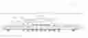
Please refer to FIG. 1. FIG. 1 is a perspective diagram illustrating a system-in-package structure 10 according to the prior art. As shown in FIG. 1, the system-in-package structure 10 includes a carrier substrate 16, in which the surface of the carrier substrate 16 defines a molding area 30 and a periphery area 32. The molding area 30 includes a chip 12 disposed on the carrier substrate 16, an adhesive layer 14 disposed between the carrier substrate 16 and the chip 12, and a molding compound 24 covering the chip 12 and part of the carrier substrate 16. Additionally, the system-in-package structure 10 includes a plurality of wires 18 electrically connected to the chip 12 and the carrier substrate 16 and a plurality of solder balls 22 disposed on the bottom surface of the carrier substrate 16, in which the solder balls 22 are connected to the chip 12 through the circuits (not shown) within the carrier substrate 16. The periphery area 32 includes a solder mask 32 and a plurality of solder pads 36 disposed on the surface of the carrier substrate 16, in which the height of the surface of the solder pads 36 is equivalent to the height of the solder mask 34 surface.
However, the molding compound 24 covering the chip 12 and the carrier substrate 16 often flush out of the molding area 30 and flood the surface of the periphery area 32 during a molding process. Since the height of the solder mask 36 surface is equal to the height of the solder pads 36 surface, excessive molding compound 24 utilized during the molding process will flood. The flood covers the solder pads 36 and the solder mask 34 in the periphery area 32 thereby influencing the ball mounting process thereafter. Consequently, the stability of the passive devices (not shown), active devices (not shown), and solder balls (not shown) disposed on the solder pads 36 is not ideal.
SUMMARY OF THE INVENTIONIt is therefore an objective of the present invention to provide a package structure having a void in the periphery of a carrier substrate to improve the problem of contamination of solder pads by the flooding of molding compound.
According to the present invention, a system-in-package structure includes a carrier substrate, in which the surface of the carrier substrate defines a molding area and a periphery area; a chip disposed in the molding area; a molding compound disposed in the molding area and covering the chip; a plurality of solder pads disposed on the surface of the carrier substrate and in the periphery area; and a solder mask disposed on the periphery area and partially covering the surface of the solder pads, in which the solder mask includes at least a void.
Preferably, the present invention provides a solder mask having a void therein in the periphery area of a carrier substrate. During the molding process the excess molding compound flushed out from the molding area is able to flow into the void and avoid contaminating the solder pads, thereby improving the yield and stability of the ball mounting process performed on the solder pads thereafter.
These and other objectives of the present invention will no doubt become obvious to those of ordinary skill in the art after reading the following detailed description of the preferred embodiment that is illustrated in the various figures and drawings.
BRIEF DESCRIPTION OF THE DRAWINGSFIG. 1 is a perspective diagram illustrating a system-in-package structure according to the prior art.
FIG. 2 and FIG. 3 are perspective diagrams illustrating a bottom package structure according to the preferred embodiment of the present invention.
FIG. 4 and FIG. 5 are perspective diagrams illustrating a system-in-package structure according to another embodiment of the present invention.
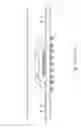
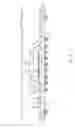
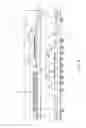
DETAILED DESCRIPTIONPlease refer to FIG. 2 and FIG. 3. FIG. 2 and FIG. 3 are perspective diagrams illustrating a bottom package structure 60 according to the preferred embodiment of the present invention. As shown in FIG. 2 and FIG. 3, the bottom package structure 60 includes a carrier substrate 62. The surface of the carrier substrate 62 defines a molding area 64 and a periphery area 66, in which the depth of the molding area 64 is greater than the depth of the periphery area 66. The bottom package structure 60 also includes at least a chip 68, positioned on the surface of the carrier substrate 62 and within the molding area 64, an adhesive layer 70 disposed between the carrier substrate 62 and the chip 68, and a molding compound 72 covering the chip 68 and part of the carrier substrate 62. Please note that the chip 68 can be, for example, a flip chip. Additionally, the bottom package structure 60 includes a plurality of wires 74 formed by wire bonding for electrically connecting the chip 68 and the carrier substrate 62, and a plurality of solder balls 76 disposed on the bottom surface of the carrier substrate 62, in which the solder balls 76 are electrically connected to the chip 68 via the circuits (not shown) inside the carrier substrate 62.
Preferably, the periphery area 66 of the bottom package structure 60 includes a solder mask 80 and a plurality of solder pads 82 disposed on the carrier substrate 62. The solder pads 82 are utilized to electrically connect other passive devices, active devices, chips, or packages in a ball mounting process. Preferably, the height of the solder pads 82 is not only greater than or equal to the height of the molding area surface, but also greater than the height of the solder mask 80 surface. The molding compound 72 and the carrier substrate 62 includes a contact surface 78 therein between, in which the contact surface 78 is lower than the solder mask 80 surface and the tip of the opening above the solder pads 82, as shown in FIG. 2, are equivalent to the tip of the opening above the solder pads 82, as shown in FIG. 3.
According to the preferred embodiment of the present invention, the solder mask 80 not only surrounds a plurality of solder pads 82 on the carrier substrate 62, but also includes a void 84, in which the void 84 is formed between the solder pads 82. Hence, if the molding compound 72 covering the chip 68 and a portion of the carrier substrate 62 flushes out of the molding area 64 during a molding process, the flooded molding compound 72 can be contained within the void 84, thereby preventing the solder pads 82 situated in the periphery area 66 from suffering from any contamination by the molding compound 72. The formation of the solder pads 82 is achieved by stacking metal layers one over another, such as first forming a first metal layer 86 on the surface of the carrier substrate 62, and then forming a second metal layer 88 on top of the first metal layer 86. The solder mask 80 can be a multi-layer solder mask, in which the solder mask 80 can be etched to form the void 84.
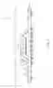
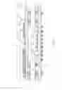
Please refer to FIG. 4 and FIG. 5. FIG. 4 and FIG. 5 are perspective diagrams illustrating a system-in-package structure 92 according to another embodiment of the present invention. As shown in FIG. 4 and FIG. 5, the present invention is able to combine the bottom package structure 60 and a top package structure 90 to form a system-in-package structure 92. As described above, the bottom package structure 60 includes a carrier substrate 62, in which the surface of the carrier substrate 62 defines a molding area 64 and a periphery area 66. The bottom package structure 60 also includes at least a chip 68, such as a flip chip positioned on the surface of the carrier substrate 62, an adhesive layer 70 disposed between the carrier substrate 62 and the chip 68, and a molding compound 72 covering the chip 68 and a portion of the carrier substrate 62. Additionally, the bottom package structure 60 includes a plurality of wires 74 formed by wire bonding for electrically connecting the chip 68 and the carrier substrate 62, and a plurality of solder balls 76 disposed on the bottom surface of the carrier substrate 62, in which the solder balls 76 are electrically connected to the chip 68 via the circuits (not shown) inside the carrier substrate 62.
The top package structure 90 includes a carrier substrate 94 and at least a chip 96 and 98 disposed on the surface of the carrier substrate 94. The chip 96 is connected to the carrier substrate 94 via a plurality of wires 102 through wire bonding, whereas the chip 98 is connected to the surface of the substrate 94 via a plurality of solder balls 100 through a flip chip packaging process. The top package structure 90 also includes a mounding compound 104 covering the chip 96 and 98, the wires 102, and the carrier substrate 94. As shown in FIG. 4, the bottom package structure 60 is connected to the top package structure 90 via a plurality of solder balls 106. Additionally, as shown in FIG. 5, the present invention is able to dispose a substrate 108 between the top package structure 90 and the bottom package structure 60, and utilize a plurality of solder balls 110 and the carrier substrate 108 to connect the bottom package structure 60 and the top package structure 90 and form the system-in-packages structure 92.
In contrast to the conventional system-in-package structure, the present invention provides a solder mask having a void therein in the periphery area of a carrier substrate, such that the excess molding compound flushed out from the molding area during the molding process is able to flow into the void and avoid contaminating the solder pads, thereby improving the yield and stability of the ball mounting process performed on the solder pads thereafter.
Those skilled in the art will readily observe that numerous modifications and alterations of the device and method may be made while retaining the teachings of the invention. Accordingly, the above disclosure should be construed as limited only by the metes and bounds of the appended claims.
Claims
What is claimed is:1. A system-in-package structure, comprising:
a carrier substrate, wherein the surface of the carrier substrate defines a molding area and a periphery area;
a chip disposed in the molding area;
a molding compound disposed in the molding area and covering the chip;
a plurality of solder pads disposed on the surface of the carrier substrate and in the periphery area; and
a solder mask disposed on the periphery area and partially exposing the surface of the solder pads, wherein the solder mask comprises at least one void.
2. The system-in-package structure of claim 1, wherein the chip is a flip chip.
3. The system-in-package structure of claim 1 further comprising a plurality of wires connecting the chip and the carrier substrate, wherein the wires are covered by the molding compound.
4. The system-in-package structure of claim 1 further comprising a plurality of solder balls disposed on the bottom surface of the carrier substrate.
5. The system-in-package structure of claim 1, wherein the depth of the molding area is greater than the depth of the periphery area.
6. The system-in-package structure of claim 1, wherein the surface of the solder pads is higher than or equal to the surface of the molding area.
7. The system-in-package structure of claim 1, wherein the surface of the solder pads is higher than or equal to the surface of the solder mask.
8. The system-in-package structure of claim 1, wherein the molding compound and the carrier substrate comprise a contacting surface, the contacting surface is lower than the solder mask, and the tip of an opening above the solder pads.
9. A system-in-package structure, comprising:
a bottom package structure, comprising:
a first carrier substrate, wherein the surface of the first carrier substrate defines a molding area and a periphery area;
a first chip disposed in the molding area;
a first molding compound disposed in the molding area and covering the first chip;
a plurality of solder pads disposed on the surface of the first carrier substrate and in the periphery area; and
a solder mask disposed on the periphery area and partially exposing the surface of the solder pads, wherein the solder mask comprises at least one void;
a top package structure, comprising:
a second carrier substrate;
a second chip disposed on the surface of the second carrier substrate;
a second molding compound covering the second chip; and
a plurality of solder balls bonding to the upper surface of the first carrier substrate and the bottom surface of the second carrier substrate.
10. The system-in-package structure of claim 9, wherein the first chip and the second chip are flip chips.
11. The system-in-package structure of claim 9, wherein the bottom package structure further comprises a plurality of wires connecting the first chip and the first carrier substrate, wherein the wires are covered by the first molding compound.
12. The system-in-package structure of claim 9, wherein the top package structure further comprises a plurality of wires connecting the second chip and the second carrier substrate, wherein the wires are covered by the second molding compound.
13. The system-in-package structure of claim 9, wherein the bottom package structure comprises a plurality of solder balls disposed on the bottom surface of the first carrier substrate.
14. The system-in-package structure of claim 9, wherein the depth of the molding area is greater than the depth of the periphery area.
15. The system-in-package structure of claim 9, wherein the surface of the solder pads is higher than or equal to the surface of the molding area.
16. The system-in-package structure of claim 9, wherein the surface of the solder pads is higher than or equal to the surface of the solder mask.
17. The system-in-package structure of claim 9 further comprising a third carrier substrate, wherein the third carrier substrate connects the bottom packages structure and the top package structure through the solder balls.
18. The system-in-package structure of claim 9, wherein the first molding compound and the first carrier substrate comprise a contacting surface, the contacting surface is lower than the solder mask, and the tip of an opening above the solder pads.
Images & Drawings included:
Sources:
- United States Patent and Trademark Office - verify current appl. status at the USPTO↗
Similar patent applications:
- » 20250253253
DUAL-SIDED ROUTING IN 3D SEMICONDUCTOR SYSTEM-IN-PACKAGE STRUCTURE AND METHODS OF FORMING THE SAME - » 20130056872
Packaging and function tests for package-on-package and system-in-package structures - » 20190103332
Wafer-level system-in-package structure and electronic apparatus thereof - » 20230387028
Dual-sided routing in 3D semiconductor system-in-package structure and methods of forming the same - » 20210407973
SYSTEM-IN-PACKAGE STRUCTURE AND PACKAGING METHOD THEREOF - » 20080001272
System-in-package structure - » 20140248722
Packaging and function tests for package-on-package and system-in-package structures - » 20160148861
FIRST-PACKAGED AND LATER-ETCHED THREE-DIMENSIONAL FLIP-CHIP SYSTEM-IN-PACKAGE STRUCTURE AND PROCESSING METHOD THEREFOR - » 20210043601
Package structure of wafer-level system-in-package - » 20190115316
Packaging method and package structure of wafer-level system-in-package
Recent applications in this class:
- » 20250286027 2025-09-11
SYSTEM PACKAGING FOR CELLULAR MODEM AND TRANSCEIVER SYSTEM OF HETEROGENEOUS STACKING - » 20250286026 2025-09-11
SEMICONDUCTOR DEVICE WITH SPACER AND METHOD FOR FABRICATING THE SAME - » 20250286025 2025-09-11
SEMICONDUCTOR DEVICE WITH SPACER AND METHOD FOR FABRICATING THE SAME - » 20250286024 2025-09-11
SEMICONDUCTOR DEVICE WITH SPACER AND METHOD FOR FABRICATING THE SAME - » 20250259975 2025-08-14
SEMICONDUCTOR PACKAGE INCLUDING REDISTRIBUTION SUBSTRATE - » 20250233117 2025-07-17
METHOD OF FORMING SEMICONDUCTOR DEVICE USING HIGH STRESS CLEAVE PLANE - » 20250210601 2025-06-26
PIXEL ARRAY AND MANUFACTURING METHOD THEREFOR - » 20250210600 2025-06-26
SYSTEM-ON-CHIP GAP FILL METHOD AND STRUCTURE - » 20250201784 2025-06-19
SEMICONDUCTOR DEVICE HAVING PACKAGE ON PACKAGE STRUCTURE AND METHOD OF MANUFACTURING THE SEMICONDUCTOR DEVICE - » 20250183237 2025-06-05
PACKAGE STRUCTURE INCLUDING A BACKSIDE METAL FILM ON A SEMICONDUCTOR DIE AND A THERMALLY CONDUCTIVE UNDERFILL LAYER ON THE BACKSIDE METAL FILM AND METHODS OF FORMING THE SAME
Recent applications for this Assignee:
- » 20080220566 2008-09-11
Substrate process for an embedded component - » 20080164545 2008-07-10
MEMS microphone package and method thereof - » 20080157238 2008-07-03
MEMS microphone module and method thereof - » 20080087987 2008-04-17
Semiconductor packaging structure having electromagnetic shielding function and method for manufacturing the same - » 20080001308 2008-01-03
Flip-chip package structure with stiffener - » 20070291458 2007-12-20
Stacked semiconductor package having flexible circuit board therein - » 20070200239 2007-08-30
Redistribution connecting structure of solder balls - » 20070138615 2007-06-21
Packaging method of a plurality of chips stacked on each other and package structure thereof - » 20070087548 2007-04-19
Method for forming bumps - » 20070087546 2007-04-19
Etchant and method for forming bumps