Vertically integrated system-in-a-package
US20060220206A1
2006-10-05
11/092,363
2005-03-29
✅ Patent granted
US 7,582,963 B2
2009-09-01
-
-
W. David Coleman | Su C Kim
2025-03-29
Abstract:
According to one embodiment of the invention, a method of forming a system-in-a-package includes providing a first substrate, coupling a first die to a top surface of the first substrate, coupling one or more surface mount devices to a top surface of a second substrate, coupling the second substrate to a top surface of the first die, interconnecting the first substrate, the second substrate, and the first die, and encapsulating the first die, the second substrate and the surface mount devices.
Inventors:
- Mark A. Gerber 7 🇺🇸 Plano, TX, United States
- Wyatt A. Huddleston 8 🇺🇸 Allen, TX, United States
- Wyatt Huddleston 2 🇺🇸 Allen, TX, United States
Assignee:
- TEXAS INSTRUMENTS INCORPORATED 18,931 🇺🇸 Dallas, TX, United States
Interested in similar patents?
Get notified when new applications in this technology area are published.
Classification:
H01L23/34 IPC
Details of semiconductor or other solid state devices Arrangements for cooling, heating, ventilating or temperature compensation ; Temperature sensing arrangements
H01L25/0657 » CPC main
Assemblies consisting of a plurality of individual semiconductor or other solid state devices ; Multistep manufacturing processes thereof all the devices being of a type provided for in the same subgroup of groups - , e.g. assemblies of rectifier diodes the devices not having separate containers the devices being of a type provided for in group Stacked arrangements of devices
H01L23/49816 » CPC further
Details of semiconductor or other solid state devices; Arrangements for conducting electric current to or from the solid state body in operation, e.g. leads, terminal arrangements ; Selection of materials therefor consisting of soldered constructions; Leads, on insulating substrates,; Additional leads joined to the metallisation on the insulating substrate, e.g. pins, bumps, wires, flat leads Spherical bumps on the substrate for external connection, e.g. ball grid arrays [BGA]
H01L24/49 » CPC further
Arrangements for connecting or disconnecting semiconductor or solid-state bodies; Methods or apparatus related thereto; Means for bonding being attached to, or being formed on, the surface to be connected, e.g. chip-to-package, die-attach, "first-level" interconnects; Manufacturing methods related thereto; Wire connectors; Manufacturing methods related thereto; Structure, shape, material or disposition of the wire connectors after the connecting process of a plurality of wire connectors
H01L25/162 » CPC further
Assemblies consisting of a plurality of individual semiconductor or other solid state devices ; Multistep manufacturing processes thereof the devices being of types provided for in two or more different main groups of - , e.g. forming hybrid circuits the devices being mounted on two or more different substrates
H01L25/50 » CPC further
Assemblies consisting of a plurality of individual semiconductor or other solid state devices ; Multistep manufacturing processes thereof Multistep manufacturing processes of assemblies consisting of devices, each device being of a type provided for in group or
H01L24/45 » CPC further
Arrangements for connecting or disconnecting semiconductor or solid-state bodies; Methods or apparatus related thereto; Means for bonding being attached to, or being formed on, the surface to be connected, e.g. chip-to-package, die-attach, "first-level" interconnects; Manufacturing methods related thereto; Wire connectors; Manufacturing methods related thereto; Structure, shape, material or disposition of the wire connectors prior to the connecting process of an individual wire connector
H01L24/48 » CPC further
Arrangements for connecting or disconnecting semiconductor or solid-state bodies; Methods or apparatus related thereto; Means for bonding being attached to, or being formed on, the surface to be connected, e.g. chip-to-package, die-attach, "first-level" interconnects; Manufacturing methods related thereto; Wire connectors; Manufacturing methods related thereto; Structure, shape, material or disposition of the wire connectors after the connecting process of an individual wire connector
H01L24/73 » CPC further
Arrangements for connecting or disconnecting semiconductor or solid-state bodies; Methods or apparatus related thereto Means for bonding being of different types provided for in two or more of groups , , , , , , ,
H01L2224/49 » CPC further
Indexing scheme for arrangements for connecting or disconnecting semiconductor or solid-state bodies and methods related thereto as covered by; Means for bonding being attached to, or being formed on, the surface to be connected, e.g. chip-to-package, die-attach, "first-level" interconnects; Manufacturing methods related thereto; Wire connectors; Manufacturing methods related thereto; Structure, shape, material or disposition of the wire connectors after the connecting process of a plurality of wire connectors
H01L2225/06506 » CPC further
Details relating to assemblies covered by the group but not provided for in its subgroups; All the devices being of a type provided for in the same subgroup of groups - the devices not having separate containers the devices being of a type provided for in group; Stacked arrangements of devices Wire or wire-like electrical connections between devices
H01L2225/0651 » CPC further
Details relating to assemblies covered by the group but not provided for in its subgroups; All the devices being of a type provided for in the same subgroup of groups - the devices not having separate containers the devices being of a type provided for in group; Stacked arrangements of devices Wire or wire-like electrical connections from device to substrate
H01L2225/06541 » CPC further
Details relating to assemblies covered by the group but not provided for in its subgroups; All the devices being of a type provided for in the same subgroup of groups - the devices not having separate containers the devices being of a type provided for in group; Stacked arrangements of devices Conductive via connections through the device, e.g. vertical interconnects, through silicon via [TSV]
H01L2225/06586 » CPC further
Details relating to assemblies covered by the group but not provided for in its subgroups; All the devices being of a type provided for in the same subgroup of groups - the devices not having separate containers the devices being of a type provided for in group; Stacked arrangements of devices; Housing for the assembly, e.g. chip scale package [CSP] Housing with external bump or bump-like connectors
H01L2924/01014 » CPC further
Indexing scheme for arrangements or methods for connecting or disconnecting semiconductor or solid-state bodies as covered by; Chemical elements Silicon [Si]
H01L2924/01032 » CPC further
Indexing scheme for arrangements or methods for connecting or disconnecting semiconductor or solid-state bodies as covered by; Chemical elements Germanium [Ge]
H01L2924/01033 » CPC further
Indexing scheme for arrangements or methods for connecting or disconnecting semiconductor or solid-state bodies as covered by; Chemical elements Arsenic [As]
H01L2924/01079 » CPC further
Indexing scheme for arrangements or methods for connecting or disconnecting semiconductor or solid-state bodies as covered by; Chemical elements Gold [Au]
H01L2924/01082 » CPC further
Indexing scheme for arrangements or methods for connecting or disconnecting semiconductor or solid-state bodies as covered by; Chemical elements Lead [Pb]
H01L2924/014 » CPC further
Indexing scheme for arrangements or methods for connecting or disconnecting semiconductor or solid-state bodies as covered by; Alloys Solder alloys
H01L2924/14 » CPC further
Indexing scheme for arrangements or methods for connecting or disconnecting semiconductor or solid-state bodies as covered by; Details of semiconductor or other solid state devices to be connected; Device type Integrated circuits
H01L2924/19041 » CPC further
Indexing scheme for arrangements or methods for connecting or disconnecting semiconductor or solid-state bodies as covered by; Details of hybrid assemblies other than the semiconductor or other solid state devices to be connected; Structure; Component type being a capacitor
H01L2924/19104 » CPC further
Indexing scheme for arrangements or methods for connecting or disconnecting semiconductor or solid-state bodies as covered by; Details of hybrid assemblies other than the semiconductor or other solid state devices to be connected; Disposition of discrete passive components in a stacked assembly with the semiconductor or solid state device on the semiconductor or solid-state device, i.e. passive-on-chip
H01L2924/19107 » CPC further
Indexing scheme for arrangements or methods for connecting or disconnecting semiconductor or solid-state bodies as covered by; Details of hybrid assemblies other than the semiconductor or other solid state devices to be connected; Disposition of discrete passive components off-chip wires
H01L2224/92247 » CPC further
Indexing scheme for arrangements for connecting or disconnecting semiconductor or solid-state bodies and methods related thereto as covered by; Methods for connecting semiconductor or solid state bodies including different methods provided for in two or more of groups - ; Specific sequence of method steps; Connecting different surfaces of the semiconductor or solid-state body with connectors of different types; Sequential connecting processes the first connecting process involving a layer connector the second connecting process involving a wire connector
H01L2924/00014 » CPC further
Indexing scheme for arrangements or methods for connecting or disconnecting semiconductor or solid-state bodies as covered by; Technical content checked by a classifier the subject-matter covered by the group, the symbol of which is combined with the symbol of this group, being disclosed without further technical details
H01L2224/73265 » CPC further
Indexing scheme for arrangements for connecting or disconnecting semiconductor or solid-state bodies and methods related thereto as covered by; Means for bonding being of different types provided for in two or more of groups; Location after the connecting process on different surfaces Layer and wire connectors
H01L2924/15787 » CPC further
Indexing scheme for arrangements or methods for connecting or disconnecting semiconductor or solid-state bodies as covered by; Details of package parts other than the semiconductor or other solid state devices to be connected; Die mounting substrate; Material with a principal constituent of the material being a non metallic, non metalloid inorganic material Ceramics, e.g. crystalline carbides, nitrides or oxides
H01L2924/00 » CPC further
Indexing scheme for arrangements or methods for connecting or disconnecting semiconductor or solid-state bodies as covered by
H01L2924/181 » CPC further
Indexing scheme for arrangements or methods for connecting or disconnecting semiconductor or solid-state bodies as covered by; Details of package parts other than the semiconductor or other solid state devices to be connected Encapsulation
H01L2924/00012 » CPC further
Indexing scheme for arrangements or methods for connecting or disconnecting semiconductor or solid-state bodies as covered by; Technical content checked by a classifier Relevant to the scope of the group, the symbol of which is combined with the symbol of this group
H01L2924/15311 » CPC further
Indexing scheme for arrangements or methods for connecting or disconnecting semiconductor or solid-state bodies as covered by; Details of package parts other than the semiconductor or other solid state devices to be connected; Die mounting substrate; Connection portion the connection portion being formed only on the surface of the substrate opposite to the die mounting surface being a ball array, e.g. BGA
H01L23/02 IPC
Details of semiconductor or other solid state devices Containers; Seals
Description
TECHNICAL FIELD OF THE INVENTIONThis invention relates generally to the field of integrated circuit packaging and, more specifically, to a vertically integrated system-in-a-package (SIP).
BACKGROUND OF THE INVENTIONElectronic devices, such as cell phones and PDA's, typically include several individually packaged integrated circuits with different functions. To facilitate space savings and, hence, significant down-sizing of electronic gadgets, 3D packaging solutions may be utilized.
One 3D packaging technique is a “System-in-a-Package” (SIP) approach. SIP refers to a semiconductor device that incorporates multiple die that make up a complete electronic system into a single package. SIP sometimes employs die stacking, which mounts die on top of one another and interconnects them.
Another form of 3-D packaging is package-in-a-package stacking. Package-in-package stacking involves flipping and stacking a tested package onto a base package, with subsequent interconnection via wire bonding. A package-in-package requires the tested package to be fully encapsulated prior to assembly within the base package.
SUMMARY OF THE INVENTIONAccording to one embodiment of the invention, a method of forming a system-in-a-package includes providing a first substrate, coupling a first die to a top surface of the first substrate, coupling one or more surface mount devices to a top surface of a second substrate, coupling the second substrate to a top surface of the first die, interconnecting the first substrate, the second substrate, and the first die, and encapsulating the first die, the second substrate and the surface mount devices.
Some embodiments of the invention provide numerous technical advantages. Other embodiments may realize some, none, or all of these advantages. For example, with SIP technology, according to one embodiment of the invention, vendors are able to reduce the footprint of integrated circuit packages. In addition, embodiments of the invention may reduce development time to bring new products to the market. The integration of passive components may be performed independently of the standard packaging process, and may be pre-fabricated at a site other than that which assembles the package.
Other technical advantages are readily apparent to one skilled in the art from the following figures, descriptions, and claims.
BRIEF DESCRIPTION OF THE DRAWINGSFor a more complete understanding of the invention, and for further features and advantages, reference is now made to the following description, taken in conjunction with the accompanying drawings, in which:
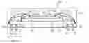
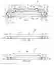
FIG. 1 is a perspective view of a system-in-a-package according to one embodiment of the invention; and
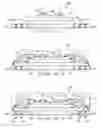
FIGS. 2A through 2E illustrate various manufacturing stages of the system-in-a-package of FIG. 1 according to one embodiment of the invention.
DETAILED DESCRIPTION OF EXAMPLE EMBODIMENTS OF THE INVENTIONExample embodiments of the present invention and their advantages are best understood by referring now to FIGS. 1 through 2E of the drawings, in which like numerals refer to like parts.
FIG. 1 is a perspective view of a system-in-a-package (“SIP”) according to one embodiment of the invention. In the illustrated embodiment, SIP 100 includes a first substrate 102, a first die 104, a second die 106, a second substrate 108, a plurality of surface mount devices 110, a plurality of wirebonds 112, a mold compound 114, a plurality of bond pads 118, and a plurality of solder balls 122. The present invention, however, contemplates more, fewer, or different components for SIP 100 than those shown in FIG. 1. One important advantage of some embodiments of the invention is that SIP 100 may provide passive component integration with a reduced footprint, which is described in further detail below.
Substrate 102, in one embodiment, is a glass-fiber-reinforced epoxy resin, such as FR4; however, substrate 102 may be formed from other suitable substrates, such as a laminate substrate, a ceramic substrate, and a polyimide substrate. Substrate 102 may also have any suitable shape and any suitable thickness. In the illustrated embodiment, substrate 102 includes a plurality of bond pads 118 formed on a top surface 103 thereof coupled to a plurality of solder balls 122 coupled to a bottom surface of substrate 102 by respective vias 124. Bond pads 118, vias 124, and solder balls 122 may be formed from any suitable material and may be arranged in any suitable manner.
First die 104 and second die 106 may be any suitable integrated circuit die having any suitable function. For example, both first die 104 and second die 106 may be formed from silicon or germanium with any suitable number and arrangement of dielectric and metal layers formed therein. First die 104 and second die 106 may also have any suitable contact pads (not explicitly illustrated) to facilitate interconnection between the various components of SIP 100. Although only two integrated circuit die 104, 106 are illustrated in FIG. 1, the present invention contemplates any suitable number of integrated circuit die being stacked on top surface 103 of substrate 102. First die 104 may couple to substrate 102 in any suitable manner, such as by a suitable epoxy. Second die 106 may couple to a top surface 105 of first die 104 via any suitable manner, such as with a film adhesive.
Substrate 108, in one embodiment, is a passive electrical carrier having surface mount devices 110 coupled to a top surface 109 thereof. Substrate 108 may be formed from any suitable substrate, such as a tape substrate, a laminate substrate, a ceramic substrate, or other suitable substrates. Substrate 108 may be coupled to a top surface 107 of second die 106 in any suitable manner, such as with a film adhesive. In a particular embodiment of the invention, substrate 108 has a plurality of solder balls (not illustrated) coupled to a bottom surface thereof that couple to top surface 107 of second die 106. In this embodiment, any suitable reflow technology may be utilized to couple substrate 108 to second die 106. Furthermore, in this particular embodiment, second die 106 may have suitable metallization formed therein that is similar to bonding over active circuitry (“BOAC”).
Surface mount devices 110 may be any suitable passive or active discrete components. In one embodiment, surface mount devices 110 include suitable passive components, such as capacitors, diodes, resistors, and inductors. Surface mount devices 110 may couple to a top surface 109 of substrate 108 in any suitable manner, such as soldering. According to the teachings of one embodiment of the invention, surface mount devices 110 are coupled to top surface 109 of substrate 108 instead of being coupled to a perimeter 120 of top surface 103 of substrate 102, as is done with some prior SIP's. This not only reduces the footprint of SIP 100, but enhances the manufacturability and reliability of SIP 100. For example, the passive integration process for surface mount devices 110 may be performed independently from the standard packaging processes for first die 104 and second die 106. In addition, substrate 108 populated with surface mount devices 110 may be pre-fabricated at a site other than the site that assembles SIP 100. The independent integration process makes it easier to change the design of substrate 108 with surface mount devices 110.
Wirebonds 112 may be any suitable wirebonds, such as gold wirebonds that couple respective components of SIP 100. For example, wirebonds 112 may couple substrate 108 to each of substrate 102, first die 104, and second die 106. In addition, both first die 104 and second die 106 may both couple to substrate 102 with suitable wirebonds. Any suitable interconnection between components of SIP 100 is contemplated by the present invention.
Mold compound 114 may be any suitable mold compound that functions to encapsulate first die 104, second die 106, substrate 108, surface mount devices 110, and wire bonds 112. For example, mold compound 114 may be a suitable epoxy, thermosetting plastic, or thermoplastic. Mold compound 114 may be formed with any suitable thickness and in any suitable configuration.
FIGS. 2A through 2E illustrate various manufacturing stages of SIP 100 according to one embodiment of the invention. Referring first to FIG. 2A, first die 104 is coupled to top surface 103 of substrate 102 in any suitable manner, such as by a suitable epoxy. Optionally, at this point in the manufacturing sequence, first die 104 may be electrically coupled to one or more bond pads 118 of first substrate 102 with suitable wirebonds 112 (not illustrated in FIG. 2A). In addition, although not illustrated in FIG. 2A, depending on the type of material used to couple first die 104 to substrate 102, a curing step may also take place at this point in the manufacturing sequence.
As illustrated in FIG. 2B, second die 106 is then coupled to top surface 105 of first die 104 in any suitable manner, such as with a film adhesive. Optionally, at this stage of the manufacturing sequence, second die 106 may be electrically coupled to one or more bond pads 118 of first substrate 102 and/or suitable bond pads on first die 104 with suitable wirebonds 112 (not explicitly illustrated in FIG. 2B). In addition, first die 104 may be electrically coupled to one or more bond pads 118 of first substrate 102 if this was not performed previously. An optional curing step may also take place at this point in the manufacturing sequence. Although not illustrated in the figures, subsequent dies may be stacked upon one another. Again, any suitable number of stacked integrated circuit die are contemplated by the present invention.
FIG. 2C illustrates substrate 108 coupled to top surface 107 of second die 106 in any suitable manner, such as with a film adhesive. In one embodiment, surface mount devices 110 are coupled to top surface 109 of substrate 108 before substrate 108 is coupled to top surface 107 of second die 106. In other words, surface mount devices 110 may be coupled to top surface 109 of second substrate 108 in parallel with the manufacturing/packaging of first die 104 and second die 106 in order to make the manufacturing of SIP 100 more efficient. Optionally, at this stage of the manufacturing sequence, second substrate 108 may be electrically coupled to one or more bond pads 118 of first substrate 102 and/or suitable bond pads on either or both of first die 104 and second die 106 with suitable wirebonds 112 (not explicitly illustrated in FIG. 2C). In addition, first die 104 and/or second die 106 may be electrically coupled to one or more bond pads 118 of first substrate 102 (or to each other) if this was not performed previously. An optional curing step may also take place at this point in the manufacturing sequence.
Referring to FIG. 2D, wirebonds 112 are shown to be interconnecting first substrate 102, first die 104, second die 106, and substrate 108. As described above, any suitable interconnection between these components are contemplated by the present invention.
After the wirebonding process is completed, the encapsulating of the components of SIP 100, as shown in FIG. 2E, is performed. As described above, any suitable mold compound 114 may be utilized. In addition, after the encapsulation of the components, a suitable curing step may take place. Solder balls 122 may then be coupled to the bottom surface of substrate 102 to complete SIP package 100 in the form of a ball grid array (“BGA”) package. In lieu of a BGA package, SIP 100 may also take the form of a pin grid array, a lead frame package, or other suitable integrated circuit package. Subsequent steps may include marking and testing of SIP 100. In addition, the present invention contemplates SIP 100 being formed integrally with many other SIPs before a suitable singulation process separates them into individual packages.
Thus, SIP 100 facilitates a vertically integrated surface mount device populated substrate into a suitable integrated circuit package. Surface mount devices 110 are vertically stacked along with the stacked integrated circuit die, which helps to reduce the footprint of SIP 100 in some embodiments.
Although embodiments of the invention and their advantages are described in detail, a person skilled in the art could make various alterations, additions, and omissions without departing from the spirit and scope of the present invention, as defined by the appended claims.
Claims
What is claimed is:1. A method of forming a system-in-a-package, comprising:
providing a first substrate;
coupling a first die to a top surface of the first substrate;
coupling one or more surface mount devices to a top surface of a second substrate;
coupling the second substrate to a top surface of the first die;
interconnecting the first substrate, the second substrate, and the first die; and
encapsulating the first die, the second substrate and the surface mount devices.
2. The method of claim 1, wherein at least some of the surface mount devices comprise passive surface mount devices.
3. The method of claim 1, wherein each of the surface mount devices is selected from the group consisting of a capacitor, a diode, a resistor, and an inductor.
4. The method of claim 1, wherein the first substrate is a printed circuit board having a plurality of bond pads coupled to a perimeter thereof that generally surround the first die.
5. The method of claim 1, wherein the first die is coupled to the first substrate with an epoxy.
6. The method of claim 1, wherein the second substrate is coupled to the first die with a film adhesive.
7. The method of claim 1, wherein the surface mount devices are coupled to the second substrate with a solder.
8. The method of claim 1, wherein interconnecting comprises wirebonding.
9. The method of claim 1, further comprising coupling a plurality of solder balls to the first substrate.
10. A system-in-a-package, comprising:
a first substrate;
a first die coupled to a top surface of the first substrate;
one or more surface mount devices coupled to a top surface of a second substrate;
the second substrate coupled to a top surface of the first die;
the first substrate, the second substrate, and the first die electrically coupled together with a plurality of wirebonds; and
the first die, the second substrate and the surface mount devices encapsulated with a mold compound.
11. The system-in-a-package of claim 10, wherein at least some of the surface mount devices comprise passive surface mount devices.
12. The system-in-a-package of claim 10, wherein each of the surface mount devices is selected from the group consisting of a capacitor, a diode, a resistor, and an inductor.
13. The system-in-a-package of claim 10, wherein the first substrate is a printed circuit board having a plurality of bond pads coupled to a perimeter thereof that generally surround the first die.
14. The system-in-a-package of claim 10, further comprising a plurality of solder balls coupled to a bottom surface of the first substrate.
15. A method of forming a system-in-a-package, comprising:
providing a first substrate;
stacking a plurality of die on a top surface of the first substrate;
coupling one or more surface mount devices to a top surface of a second substrate;
coupling the second substrate to a top surface of the uppermost die of the stacked die;
interconnecting the second substrate to the first substrate and at least one of the stacked die; and
encapsulating the stacked die, the second substrate and the surface mount devices.
16. The method of claim 15, wherein at least some of the surface mount devices comprise passive surface mount devices.
17. The method of claim 15, wherein each of the surface mount devices is selected from the group consisting of a capacitor, a diode, a resistor, and an inductor.
18. The method of claim 15, wherein the first substrate is a printed circuit board having a plurality of bond pads coupled to a perimeter thereof that generally surround the stacked die.
19. The method of claim 15, wherein interconnecting comprises wirebonding.
20. The method of claim 15, further comprising coupling a plurality of solder balls to a bottom surface of the first substrate.
Images & Drawings included:
Sources:
- United States Patent and Trademark Office - verify current appl. status at the USPTO↗
Recent applications in this class:
- » 20250293212 2025-09-18
SEMICONDUCTOR PACKAGES - » 20250293211 2025-09-18
HEAT DISSIPATION FOR STACKED INTEGRATED CIRCUIT DEVICES - » 20250293210 2025-09-18
SYSTEMS AND METHODS FOR PACKAGING A SEMICONDUCTOR DEVICE - » 20250286021 2025-09-11
SEMICONDUCTOR PACKAGE - » 20250286020 2025-09-11
SEMICONDUCTOR BONDING STRUCTURE - » 20250286019 2025-09-11
SEMICONDUCTOR PACKAGE - » 20250286018 2025-09-11
METHOD OF FABRICATING SEMICONDUCTOR BONDING STRUCTURE - » 20250286017 2025-09-11
SEMICONDUCTOR DEVICE - » 20250279399 2025-09-04
SEMICONDUCTOR DEVICES AND MANUFACTURING METHODS OF THE SAME - » 20250279398 2025-09-04
VERTICAL INTERCONNECT STRUCTURES IN THREE-DIMENSIONAL INTEGRATED CIRCUITS
Recent applications for this Assignee:
- » 20250291595 2025-09-18
CIRCUIT, SYSTEM, AND METHOD FOR MATRIX DECIMATION - » 20250286550 2025-09-11
TRANSISTOR SHUTDOWN CIRCUT - » 20250279725 2025-09-04
CONDUCTION MODE CONTROL - » 20250274138 2025-08-28
SWITCH REGULATOR - » 20250267687 2025-08-21
ENHANCED BROADCAST TRANSMISSION IN UNSLOTTED CHANNEL HOPPING MEDIUM ACCESS CONTROL - » 20250266825 2025-08-21
BOOTSTRAP CIRCUIT - » 20250247097 2025-07-31
LEVEL SHIFTER CIRCUIT - » 20250247082 2025-07-31
LOW AREA AND POWER MULTI-BIT FLIP-FLOP - » 20250246995 2025-07-31
SWITCHING CONVERTER DEADTIME CONTROL - » 20250246345 2025-07-31
TRIMMING RESISTOR USING MODULATED SIGNAL