Semiconductor device
US20060231934A1
2006-10-19
11/404,934
2006-04-14
✅ Patent granted
US 7,768,102 B2
2010-08-03
-
-
Sue Purvis | Leslie Pilar Cruz
2026-11-01
Abstract:
Decrease in parasitic resistance caused by paste for adhering a semiconductor device to a lead frame or by a semiconductor substrate is disclosed. In a semiconductor device having a semiconductor substrate with an electrode formed on a rear surface thereof, an uneven structure is formed on the rear surface of the semiconductor substrate, and the rear surface electrode is formed and is adhered to a lead frame, thereby decreasing parasitic resistance and improving driving capability.
Assignee:
- Seiko Instruments Inc. 772 🇯🇵 , Japan
Interested in similar patents?
Get notified when new applications in this technology area are published.
Classification:
H01L29/06 IPC
Semiconductor devices adapted for rectifying, amplifying, oscillating or switching, or capacitors or resistors with at least one potential-jump barrier or surface barrier, e.g. PN junction depletion layer or carrier concentration layer; Details of semiconductor bodies or of electrodes thereof; Multistep manufacturing processes therefor; Semiconductor bodies ; Multistep manufacturing processes therefor characterised by their shape; characterised by the shapes, relative sizes, or dispositions of the semiconductor regions ; characterised by the concentration or distribution of impurities within semiconductor regions
H01L24/32 » CPC further
Arrangements for connecting or disconnecting semiconductor or solid-state bodies; Methods or apparatus related thereto; Means for bonding being attached to, or being formed on, the surface to be connected, e.g. chip-to-package, die-attach, "first-level" interconnects; Manufacturing methods related thereto; Layer connectors, e.g. plate connectors, solder or adhesive layers; Manufacturing methods related thereto; Structure, shape, material or disposition of the layer connectors after the connecting process of an individual layer connector
H01L24/83 » CPC further
Arrangements for connecting or disconnecting semiconductor or solid-state bodies; Methods or apparatus related thereto; Methods for connecting semiconductor or other solid state bodies using means for bonding being attached to, or being formed on, the surface to be connected using a layer connector
H01L29/0657 » CPC further
Semiconductor devices adapted for rectifying, amplifying, oscillating or switching, or capacitors or resistors with at least one potential-jump barrier or surface barrier, e.g. PN junction depletion layer or carrier concentration layer; Details of semiconductor bodies or of electrodes thereof; Multistep manufacturing processes therefor; Semiconductor bodies ; Multistep manufacturing processes therefor characterised by their shape; characterised by the shapes, relative sizes, or dispositions of the semiconductor regions ; characterised by the concentration or distribution of impurities within semiconductor regions characterised by the shape of the body
H01L29/41766 » CPC further
Semiconductor devices adapted for rectifying, amplifying, oscillating or switching, or capacitors or resistors with at least one potential-jump barrier or surface barrier, e.g. PN junction depletion layer or carrier concentration layer; Details of semiconductor bodies or of electrodes thereof; Multistep manufacturing processes therefor; Electrodes ; Multistep manufacturing processes therefor characterised by their shape, relative sizes or dispositions carrying the current to be rectified, amplified or switched; Source or drain electrodes for field effect devices with at least part of the source or drain electrode having contact below the semiconductor surface, e.g. the source or drain electrode formed at least partially in a groove or with inclusions of conductor inside the semiconductor
H01L29/045 » CPC further
Semiconductor devices adapted for rectifying, amplifying, oscillating or switching, or capacitors or resistors with at least one potential-jump barrier or surface barrier, e.g. PN junction depletion layer or carrier concentration layer; Details of semiconductor bodies or of electrodes thereof; Multistep manufacturing processes therefor; Semiconductor bodies ; Multistep manufacturing processes therefor characterised by their crystalline structure, e.g. polycrystalline, cubic or particular orientation of crystalline planes by their particular orientation of crystalline planes
H01L2224/81903 » CPC further
Indexing scheme for arrangements for connecting or disconnecting semiconductor or solid-state bodies and methods related thereto as covered by; Methods for connecting semiconductor or other solid state bodies using means for bonding being attached to, or being formed on, the surface to be connected using a bump connector with the bump connector not providing any mechanical bonding; Pressing the bump connector against the bonding areas by means of another connector by means of a layer connector
H01L2224/838 » CPC further
Indexing scheme for arrangements for connecting or disconnecting semiconductor or solid-state bodies and methods related thereto as covered by; Methods for connecting semiconductor or other solid state bodies using means for bonding being attached to, or being formed on, the surface to be connected using a layer connector Bonding techniques
H01L2224/83851 » CPC further
Indexing scheme for arrangements for connecting or disconnecting semiconductor or solid-state bodies and methods related thereto as covered by; Methods for connecting semiconductor or other solid state bodies using means for bonding being attached to, or being formed on, the surface to be connected using a layer connector; Bonding techniques using a polymer adhesive, e.g. an adhesive based on silicone, epoxy, polyimide, polyester being an anisotropic conductive adhesive
H01L2924/01005 » CPC further
Indexing scheme for arrangements or methods for connecting or disconnecting semiconductor or solid-state bodies as covered by; Chemical elements Boron [B]
H01L2924/01006 » CPC further
Indexing scheme for arrangements or methods for connecting or disconnecting semiconductor or solid-state bodies as covered by; Chemical elements Carbon [C]
H01L2924/01033 » CPC further
Indexing scheme for arrangements or methods for connecting or disconnecting semiconductor or solid-state bodies as covered by; Chemical elements Arsenic [As]
H01L2924/01082 » CPC further
Indexing scheme for arrangements or methods for connecting or disconnecting semiconductor or solid-state bodies as covered by; Chemical elements Lead [Pb]
H01L2924/0781 » CPC further
Indexing scheme for arrangements or methods for connecting or disconnecting semiconductor or solid-state bodies as covered by; Polymers; Adhesive characteristics other than chemical being an ohmic electrical conductor
H01L2924/00011 » CPC further
Indexing scheme for arrangements or methods for connecting or disconnecting semiconductor or solid-state bodies as covered by; Technical content checked by a classifier Not relevant to the scope of the group, the symbol of which is combined with the symbol of this group
H01L2224/29075 » CPC further
Indexing scheme for arrangements for connecting or disconnecting semiconductor or solid-state bodies and methods related thereto as covered by; Means for bonding being attached to, or being formed on, the surface to be connected, e.g. chip-to-package, die-attach, "first-level" interconnects; Manufacturing methods related thereto; Layer connectors, e.g. plate connectors, solder or adhesive layers; Manufacturing methods related thereto; Structure, shape, material or disposition of the layer connectors prior to the connecting process of an individual layer connector; Core members of the layer connector Plural core members
H01L2924/00014 » CPC further
Indexing scheme for arrangements or methods for connecting or disconnecting semiconductor or solid-state bodies as covered by; Technical content checked by a classifier the subject-matter covered by the group, the symbol of which is combined with the symbol of this group, being disclosed without further technical details
H01L2924/13091 » CPC further
Indexing scheme for arrangements or methods for connecting or disconnecting semiconductor or solid-state bodies as covered by; Details of semiconductor or other solid state devices to be connected; Device type; Discrete devices, e.g. 3 terminal devices; Transistor; Field-effect transistor [FET] Metal-Oxide-Semiconductor Field-Effect Transistor [MOSFET]
H01L2924/00 » CPC further
Indexing scheme for arrangements or methods for connecting or disconnecting semiconductor or solid-state bodies as covered by
H01L23/495 IPC
Details of semiconductor or other solid state devices; Arrangements for conducting electric current to or from the solid state body in operation, e.g. leads, terminal arrangements ; Selection of materials therefor consisting of soldered constructions Lead-frames or other flat leads
Description
BACKGROUND OF THE INVENTION1. Field of the Invention
The present invention relates to a semiconductor device to which high driving capability is required, and more particularly, to an improvement of driving capability of a transistor formed in a semiconductor device.
2. Description of the Related Art.
A semiconductor device is manufactured by forming a large number of semiconductor chips on a semiconductor substrate and separating the semiconductor chips from one another to be settled in a package or the like for use. Along with development in manufacturing technology for a semiconductor device, the performance of transistors formed on a surface of the semiconductor chip has been improved in various aspects. With regard to a transistor with high driving capability, which can supply power to a load that requires large electric power, various technologies have been developed to decrease ON resistance (internal resistance of the transistor when the transistor is turned on). Currently, vertical double diffused MOS transistors (VDMOS) and trench gated MOS (UMOS) transistors, each having a structure in which electric current flows perpendicularly to the surface of a semiconductor substrate, are predominantly used for decreasing the ON resistance.
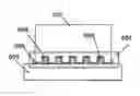
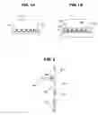
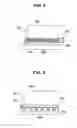
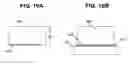
FIG. 10A is a sectional view of a semiconductor chip 009 in which a conventional transistor having high driving capability is formed. FIG. 10B is a sectional view of a conventional semiconductor device where a rear surface of the semiconductor chip 009 having a rear face electrode 004 is adhered through conductive paste 006 to a lead frame 005 that is used for packing the semiconductor chip 009. FIG. 2 is an equivalent circuit diagram (not shown in FIG. 10) of a transistor formed on an upper surface of the semiconductor chip 009 of FIG. 10. A source 016 of a transistor 011 is electrically connected to the rear surface electrode 004 of the semiconductor chip 009 via a semiconductor substrate forming the semiconductor chip 009, and power is supplied to the source 016 from the rear surface electrode 004 of the semiconductor chip 009. According to a control signal applied to a gate 014 of the transistor 011, power is supplied to a load (not shown) connected to a drain 015. Power is supplied to the source 016 of the transistor 011 of FIG. 2 from a surface 017 of the lead frame via a paste resistance 013 due to the conductive paste and a substrate resistance 012 (hereinafter the paste resistance 013 and the substrate resistance 012 are collectively referred to simply as parasitic resistance). The paste resistance 013 is the resistance of the conductive paste for adhering the semiconductor chip 009 to the lead frame 005. The substrate resistance 012 is the resistance of the semiconductor substrate which forms the semiconductor chip disposed between the rear surface electrode 004 to the source 016 of the transistor 011 and having a thickness D.
Conventionally, it was sufficient to decrease only the ON resistance, which was high as compared to the parasitic resistance, to supply high electric power to the load. However, in the above-described vertical device, despite the reduction in the ON resistance due to a development in micro fabrication technology, the parasitic resistance remains unchanged, and thus, the parasitic resistance is no longer negligible as an error in the ON resistance. In order to solve the problem, there has been adopted a back grind method for decreasing the thickness of the semiconductor substrate to decrease the substrate resistance 012 (see JP 2004-022899 A) and another method for decreasing of the paste resistance 013 through development of low resistance paste or the like (see JP 2003-016838 A).
The back grind method is to decrease the thickness D of the semiconductor substrate, as shown in FIG. 2A, but an excessive thinning in the thickness D causes lowering in the physical strength, which leads to a breaking of the semiconductor chip 009. Even if the above-described low resistance paste is used, the paste resistance 013 is more or less added serially as illustrated in FIG. 2, and thus the paste resistance can be decreased only to a certain extent. Here a problem occurs that the parasitic resistance cannot be decreased so much as compared to the ON resistance which was decreased remarkably due to the conventional art.
SUMMARY OF THE INVENTIONIn order to solve the above-mentioned problem, the present invention provides the following means:
(1) A semiconductor device including a semiconductor chip having a rear surface electrode provided on a rear surface thereof, in which the rear surf ace of the semiconductor chip includes a uneven structure having concave and convex.
(2) A semiconductor device according to the above item (1), in which the uneven structure has a stripe pattern.
(3) A semiconductor device according to the above item (1), in which the uneven structure has a lattice pattern.
(4) A semiconductor device according to the above item (1), in which the uneven structure has a nonlinear pattern.
(5) A semiconductor device according to any one of the above items (1) to (4), in which the pattern of the uneven structure is in parallel with a crystal orientation of <100> of a semiconductor substrate.
(6) A semiconductor device including a semiconductor chip having a rear surface electrode provided on a rear surface thereof, in which a lower surface of the rear surface electrode includes an uneven structure having concave and convex.
(7) A semiconductor device according to the above item (6), in which the uneven structure has a stripe pattern.
(8) A semiconductor device according to the above item (6), in which the uneven structure has a lattice pattern.
(9) A semiconductor device according to the above item (6), in which the uneven structure has a nonlinear pattern.
(10) A semiconductor device including: a semiconductor chip having a rear surface electrode provided on a rear surface thereof; and a lead frame that is in contact with the rear surface electrode, in which a surface of the lead frame includes an uneven structure having concave and convex.
(11) A semiconductor device according to the above item (10), in which the uneven structure has a stripe pattern.
(12) A semiconductor device according to the above item (10), in which the uneven structure has a lattice pattern.
(13) A semiconductor device according to the above item (10), in which the uneven structure has a nonlinear pattern.
BRIEF DESCRIPTION OF THE DRAWINGSIn the accompanying drawings:
FIG. 1A is a sectional view of a semiconductor device according to a first embodiment of the present invention;
FIG. 1B is a sectional view of the semiconductor device shown in FIG. 1A adhered to a lead frame;
FIG. 2 is an equivalent circuit diagram of a transistor of the semiconductor device;
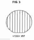
FIG. 3 is a plan view illustrating a pattern of an uneven structure according to the present invention;
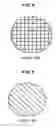
FIG. 4 is a plan view illustrating another pattern of the uneven structure according to the present invention;
FIG. 5 is a plan view illustrating another pattern of the uneven structure according to the present invention;
FIG. 6 is a plan view illustrating another pattern of the uneven structure according to the present invention;
FIG. 7 is a plan view illustrating another pattern of the uneven structure according to the present invention;
FIG. 8 is a sectional view of a semiconductor device according to a second embodiment of the present invention;
FIG. 9 is a sectional view of a semiconductor device according to a third embodiment of the present invention;
FIG. 10A is a sectional view of a conventional semiconductor device; and
FIG. 10B is a sectional view of the semiconductor device shown in FIG. 10A attached to a lead frame.
DETAILED DESCRIPTION OF THE PREFERRED EMBODIMENTSFIGS. 1A and 1B illustrate a first embodiment of the present invention. In FIG. 1A an uneven structure having concave and convex 001 is provided on a rear surface of a semiconductor chip 002 whose back side has been ground and a rear surface electrode 004 made of metal is formed on the surface of the uneven structure 001. In FIG. 1B the substrate illustrated in FIG. 1A is adhered to a lead frame 005 through conductive paste 006.
By providing the uneven structure 001 at a portion where the semiconductor chip 002 and the lead frame 005 are in contact with each other, since the substrate resistance in a direction perpendicular to a surface of the substrate is decreased, the parasitic resistance can be decreased, and also the physical strength of the semiconductor chip 002 can be increased as compared to a conventional method where the back side of the semiconductor chip 009 is ground to decrease the thickness of the semiconductor chip 009 for the purpose of decreasing the substrate resistance 012 Further, in packaging, when the semiconductor chip 002 is adhered to the lead frame 005 through the conductive paste 006, the uneven structure 001 shows an effect similar to that of tread of a tire in rain, that is as illustrated in FIG. 1B, the conductive paste 006 burrows its way into recessed portions of the uneven structure 001 allowing protruding portions of the uneven structure 001 to directly contact with the lead frame 005, which makes it possible for the semiconductor chip 002 and the lead frame 005 to contact with each other at the protruding portions without having parasitic resistance of the conductive paste 006 therebetween. Therefore, as compared with a conventional method where the thin conductive paste 006 is sandwiched between the rear surface electrode 004 and the lead frame 005, the parasitic resistance is remarkably decreased.
Embodiment 1FIG. 1A and 1B illustrate the first embodiment of the present invention. FIG. 1A illustrates a state where, the uneven structure 001 is provided on the rear surface of the semiconductor chip 002, and the rear surface electrode 004 is formed thereon. FIG. 1B illustrates a state where the semiconductor chip 002 illustrated in FIG. 1A is adhered to the lead frame 005 through the conductive paste 006.
FIGS. 3 and 4 are plan views of wafer-like semiconductor substrates each having a water flat (hereinafter referred to as WP) with a crystal orientation of <110> before being separated into semiconductor chips seen from the rear surfaces of the wafer-like semiconductor substrates with the WF at the bottom. The uneven structure 001 formed on the rear surface of the semiconductor substrate is preferably in a stripe pattern as illustrated in FIG. 3 or in a lattice pattern as illustrated in FIG. 4. When the semiconductor chip 002 is required to have more physical strength, a wafer-like semiconductor substrate with a crystal orientation of <110> is used and the uneven structure 001 is tilted by 45 degrees with respect to the WF, as shown in FIG. 5 or 6, so as to be in parallel with the crystal orientation of <110>, to thereby increase the strength of the semiconductor chip more than that of the semiconductor chip 002 formed on the semiconductor substrate provided with the uneven structure 001 illustrated in FIG. 3 or FIG. 4. Further, as illustrated in FIG. 7, it is also possible to form the uneven structure 001 into wavelike lines so as to have a nonlinear pattern to further increase the strength.
Embodiment 2By providing the uneven structure 001 on a lower surface of the rear surface electrode which is to be in contact with the lead frame 005, as illustrated in FIG. 8, instead of on the rear surface side of the wafer-like semiconductor substrate, an effect of decreasing the parasitic resistance similar to that of Embodiment 1 can be obtained, thereby making it possible to decrease the paste resistance 013.
Embodiment 3When the substrate resistance 012 is negligible, the uneven structure 001 can be provided on an upper surface of the lead frame 005 which is to be in contact with the semiconductor chip 002 as illustrated in FIG. 9, to thereby decrease the parasitic resistance.
The present invention is not limited to the above-described embodiments, and various changes and modifications maybe made within the gist of the present invention.
Claims
What is claimed is:1. A semiconductor device, comprising:
a semiconductor chip;
a rear surface of the semiconductor chip comprising an uneven structure having a concave and a convex; and
the rear surface electrode disposed along the uneven structure.
2. A semiconductor device according to claim 1, wherein the uneven structure has a stripe pattern.
3. A semiconductor device according to claim 1, wherein the uneven structure has a lattice pattern.
4. A semiconductor device according to claim 1, wherein the uneven structure has a nonlinear pattern.
5. A semiconductor device according to claim 2, wherein the pattern of the uneven structure is in parallel to a crystal orientation of <110> of a semiconductor substrate.
6. A semiconductor device, comprising a semiconductor chip having a rear surface electrode provided on a rear surface thereof, wherein a lower surface of the rear surface electrode comprises an uneven structure having a concave and a convex.
7. A semiconductor device according to claim 6, wherein the uneven structure has a stripe pattern.
8. A semiconductor device according to claim 6, wherein the uneven structure has a lattice pattern.
9. A semiconductor device according to claim 6, wherein the uneven structure has a nonlinear pattern.
10. A semiconductor device comprising:
a semiconductor chip having a rear surface electrode provided on a rear surface thereof;
a lead frame contacting with the rear surface electrode; and
a surface of the lead frame comprising an uneven structure having a concave and a convex.
11. A semiconductor device according to claim 10, wherein the uneven structure has a stripe pattern.
12. A semiconductor device according to claim 10, wherein the uneven structure has a lattice pattern.
13. A semiconductor device according to claim 10, wherein the uneven structure has a nonlinear pattern.
Images & Drawings included:

Sources:
- United States Patent and Trademark Office - verify current appl. status at the USPTO↗
Similar patent applications:
- » 20110037176
METHOD OF MANUFACTURING A SEMICONDUCTOR DEVICE MODULE, SEMICONDUCTOR DEVICE CONNECTING DEVICE, SEMICONDUCTOR DEVICE MODULE MANUFACTURING DEVICE, SEMICONDUCTOR DEVICE MODULE - » 20230162992
METHOD FOR MANUFACTURING SEMICONDUCTOR DEVICE, METHOD FOR MANUFACTURING DEVICE PROVIDED WITH SEMICONDUCTOR DEVICE, SEMICONDUCTOR DEVICE, AND DEVICE PROVIDED WITH SEMICONDUCTOR DEVICE - » 10889015
Attaching device for mounting and fixing a semiconductor device and a heat sink provided on the semiconductor device on a board, a mount board having the board, the semiconductor device, and the heat sink, and an attaching method of the semiconductor device and the heat sink provided on the semiconductor device on the board - » 20130062745
Semiconductor device, semiconductor device manufacturing method, semiconductor device mounting structure and power semiconductor device - » 20070001197
SEMICONDUCTOR DEVICE, SEMICONDUCTOR DEVICE DESIGN METHOD, SEMICONDUCTOR DEVICE DESIGN METHOD RECORDING MEDIUM, AND SEMICONDUCTOR DEVICE DESIGN SUPPORT SYSTEM - » 10600737
Semiconductor device, semiconductor device design method, semiconductor device design method recording medium, and semiconductor device design support system - » 20130168734
Epitaxial substrate for semiconductor device, semiconductor device, method of manufacturing epitaxial substrate for semiconductor device, and method of manufacturing semiconductor device - » 20110266660
Insulating film for semiconductor device, process and apparatus for producing insulating film for semiconductor device, semiconductor device, and process for producing the semiconductor device - » 20130207111
SEMICONDUCTOR DEVICE, DISPLAY DEVICE INCLUDING SEMICONDUCTOR DEVICE, ELECTRONIC DEVICE INCLUDING SEMICONDUCTOR DEVICE, AND METHOD FOR MANUFACTURING SEMICONDUCTOR DEVICE - » 20170338352
Semiconductor device, display device including semiconductor device, electronic device including semiconductor device, and method for manufacturing semiconductor device
Recent applications in this class:
- » 20250022949 2025-01-16
POWER SEMICONDUCTOR DEVICE, POWER SEMICONDUCTOR MODULE, POWER CONVERTER INCLUDING SAME, AND MANUFACTURING METHOD THEREOF - » 20240405119 2024-12-05
SILICON CARBIDE POWER SEMICONDUCTOR DEVICE - » 20240395924 2024-11-28
POWER ELECTRONIC DEVICE WITH IMPROVED ELECTRICAL PERFORMANCES - » 20240387721 2024-11-21
SILICON CARBIDE DEVICE WITH TRANSISTOR CELL AND CLAMP REGION - » 20240313104 2024-09-19
SEMICONDUCTOR DEVICE - » 20240313103 2024-09-19
VERTICAL MOSFET DEVICE AND METHOD OF MANUFACTURING VERTICAL MOSFET DEVICE - » 20240274707 2024-08-15
Manufacturing method of semiconductor device - » 20240274706 2024-08-15
SEMICONDUCTOR SWITCHING DEVICE - » 20240222492 2024-07-04
METHOD FOR PRODUCING A VERTICAL POWER SEMICONDUCTOR COMPONENT, AND VERTICAL POWER SEMICONDUCTOR COMPONENT - » 20240222491 2024-07-04
SILICON-CARBIDE-BASED MOSFET DEVICE AND METHOD FOR MANUFACTURING SAME
Recent applications for this Assignee:
- » 20190264742 2019-08-29
Method of manufacturing an enveloping layer-coated slide bearing - » 20190025766 2019-01-24
Timepiece, timepiece system, and method of controlling timepiece - » 20180306243 2018-10-25
Rolling bearing - » 20180306242 2018-10-25
Structure with thermoplastic elastomer enveloping layer, bearing, and drive module - » 20180306240 2018-10-25
Enveloping layer-coated slide bearing and drive module - » 20180241280 2018-08-23
Vibration generation device and electronic device - » 20180203417 2018-07-19
Timepiece - » 20180097302 2018-04-05
Portable printer - » 20170331349 2017-11-16
Vibration generation device and electronic apparatus - » 20170315509 2017-11-02
Mechanical component, mechanical component manufacturing method, movement, and timepiece