Electronic circuit protection device
US20060273813A1
2006-12-07
11/407,855
2006-04-20
✅ Patent granted
US 7,282,906 B2
2007-10-16
-
-
Paresh Patel
2026-04-20
Abstract:
A device for protecting an electronic circuit comprising a support to which are attached at least two circuit portions, each comprising at least one integrated circuit chip. The device comprises a wafer of a semiconductor material covered with a conductive layer arranged parallel to the support, the wafer being connected to the support by conductive pillars distributed around each circuit portion and in contact with the conductive layer.
Assignee:
- STMICROELECTRONICS SA 1,955 🇫🇷 Montrouge, France
Interested in similar patents?
Get notified when new applications in this technology area are published.
Classification:
H01L23/552 » CPC main
Details of semiconductor or other solid state devices Protection against radiation, e.g. light or electromagnetic waves
H01L23/055 » CPC further
Details of semiconductor or other solid state devices; Containers; Seals characterised by the shape of the container or parts, e.g. caps, walls the container being a hollow construction and having an insulating or insulated base as a mounting for the semiconductor body the leads having a passage through the base
H01L23/06 » CPC further
Details of semiconductor or other solid state devices; Containers; Seals characterised by the material of the container or its electrical properties
H01L23/49816 » CPC further
Details of semiconductor or other solid state devices; Arrangements for conducting electric current to or from the solid state body in operation, e.g. leads, terminal arrangements ; Selection of materials therefor consisting of soldered constructions; Leads, on insulating substrates,; Additional leads joined to the metallisation on the insulating substrate, e.g. pins, bumps, wires, flat leads Spherical bumps on the substrate for external connection, e.g. ball grid arrays [BGA]
H01L25/0655 » CPC further
Assemblies consisting of a plurality of individual semiconductor or other solid state devices ; Multistep manufacturing processes thereof all the devices being of a type provided for in the same subgroup of groups - , e.g. assemblies of rectifier diodes the devices not having separate containers the devices being of a type provided for in group the devices being arranged next to each other
H01L25/18 » CPC further
Assemblies consisting of a plurality of individual semiconductor or other solid state devices ; Multistep manufacturing processes thereof the devices being of types provided for in two or more different subgroups of the same main group of groups -
H01L25/50 » CPC further
Assemblies consisting of a plurality of individual semiconductor or other solid state devices ; Multistep manufacturing processes thereof Multistep manufacturing processes of assemblies consisting of devices, each device being of a type provided for in group or
H05K1/0218 » CPC further
Printed circuits; Details; Electrical arrangements not otherwise provided for; Reduction of cross-talk, noise or electromagnetic interference by printed shielding conductors, ground planes or power plane
H05K1/0218 » CPC further
Printed circuits; Details; Electrical arrangements not otherwise provided for; Reduction of cross-talk, noise or electromagnetic interference by printed shielding conductors, ground planes or power plane
H05K9/0022 » CPC further
Screening of apparatus or components against electric or magnetic fields; Casings with localised screening of components mounted on printed circuit boards [PCB]
H05K9/0022 » CPC further
Screening of apparatus or components against electric or magnetic fields; Casings with localised screening of components mounted on printed circuit boards [PCB]
H01L23/3128 » CPC further
Details of semiconductor or other solid state devices; Encapsulations, e.g. encapsulating layers, coatings, e.g. for protection characterised by the arrangement or shape the device being completely enclosed a substrate forming part of the encapsulation the substrate having spherical bumps for external connection
H01L24/45 » CPC further
Arrangements for connecting or disconnecting semiconductor or solid-state bodies; Methods or apparatus related thereto; Means for bonding being attached to, or being formed on, the surface to be connected, e.g. chip-to-package, die-attach, "first-level" interconnects; Manufacturing methods related thereto; Wire connectors; Manufacturing methods related thereto; Structure, shape, material or disposition of the wire connectors prior to the connecting process of an individual wire connector
H01L24/48 » CPC further
Arrangements for connecting or disconnecting semiconductor or solid-state bodies; Methods or apparatus related thereto; Means for bonding being attached to, or being formed on, the surface to be connected, e.g. chip-to-package, die-attach, "first-level" interconnects; Manufacturing methods related thereto; Wire connectors; Manufacturing methods related thereto; Structure, shape, material or disposition of the wire connectors after the connecting process of an individual wire connector
H01L24/73 » CPC further
Arrangements for connecting or disconnecting semiconductor or solid-state bodies; Methods or apparatus related thereto Means for bonding being of different types provided for in two or more of groups , , , , , , ,
H01L25/0652 » CPC further
Assemblies consisting of a plurality of individual semiconductor or other solid state devices ; Multistep manufacturing processes thereof all the devices being of a type provided for in the same subgroup of groups - , e.g. assemblies of rectifier diodes the devices not having separate containers the devices being of a type provided for in group the devices being arranged next and on each other, i.e. mixed assemblies
H01L2224/73207 » CPC further
Indexing scheme for arrangements for connecting or disconnecting semiconductor or solid-state bodies and methods related thereto as covered by; Means for bonding being of different types provided for in two or more of groups; Location after the connecting process on the same surface Bump and wire connectors
H01L2924/01079 » CPC further
Indexing scheme for arrangements or methods for connecting or disconnecting semiconductor or solid-state bodies as covered by; Chemical elements Gold [Au]
H01L2924/15331 » CPC further
Indexing scheme for arrangements or methods for connecting or disconnecting semiconductor or solid-state bodies as covered by; Details of package parts other than the semiconductor or other solid state devices to be connected; Die mounting substrate; Connection portion the connection portion being formed on the die mounting surface of the substrate the connection portion being formed both on the die mounting surface of the substrate and outside the die mounting surface of the substrate being a ball array, e.g. BGA
H01L2924/16152 » CPC further
Indexing scheme for arrangements or methods for connecting or disconnecting semiconductor or solid-state bodies as covered by; Details of package parts other than the semiconductor or other solid state devices to be connected; Cap; Shape Cap comprising a cavity for hosting the device, e.g. U-shaped cap
H05K3/284 » CPC further
Apparatus or processes for manufacturing printed circuits; Secondary treatment of printed circuits; Applying non-metallic protective coatings for encapsulating mounted components
H05K3/284 » CPC further
Apparatus or processes for manufacturing printed circuits; Secondary treatment of printed circuits; Applying non-metallic protective coatings for encapsulating mounted components
H05K2203/041 » CPC further
Indexing scheme relating to apparatus or processes for manufacturing printed circuits covered by; Soldering or other types of metallurgic bonding Solder preforms in the shape of solder balls
H05K2203/041 » CPC further
Indexing scheme relating to apparatus or processes for manufacturing printed circuits covered by; Soldering or other types of metallurgic bonding Solder preforms in the shape of solder balls
H01L2924/15311 » CPC further
Indexing scheme for arrangements or methods for connecting or disconnecting semiconductor or solid-state bodies as covered by; Details of package parts other than the semiconductor or other solid state devices to be connected; Die mounting substrate; Connection portion the connection portion being formed only on the surface of the substrate opposite to the die mounting surface being a ball array, e.g. BGA
H01L2224/73265 » CPC further
Indexing scheme for arrangements for connecting or disconnecting semiconductor or solid-state bodies and methods related thereto as covered by; Means for bonding being of different types provided for in two or more of groups; Location after the connecting process on different surfaces Layer and wire connectors
H01L2924/00012 » CPC further
Indexing scheme for arrangements or methods for connecting or disconnecting semiconductor or solid-state bodies as covered by; Technical content checked by a classifier Relevant to the scope of the group, the symbol of which is combined with the symbol of this group
H01L2924/14 » CPC further
Indexing scheme for arrangements or methods for connecting or disconnecting semiconductor or solid-state bodies as covered by; Details of semiconductor or other solid state devices to be connected; Device type Integrated circuits
H01L2924/00 » CPC further
Indexing scheme for arrangements or methods for connecting or disconnecting semiconductor or solid-state bodies as covered by
H01L2924/207 » CPC further
Indexing scheme for arrangements or methods for connecting or disconnecting semiconductor or solid-state bodies as covered by; Parameters Diameter ranges
H01L2924/00014 » CPC further
Indexing scheme for arrangements or methods for connecting or disconnecting semiconductor or solid-state bodies as covered by; Technical content checked by a classifier the subject-matter covered by the group, the symbol of which is combined with the symbol of this group, being disclosed without further technical details
H01L2924/00011 » CPC further
Indexing scheme for arrangements or methods for connecting or disconnecting semiconductor or solid-state bodies as covered by; Technical content checked by a classifier Not relevant to the scope of the group, the symbol of which is combined with the symbol of this group
H01L2224/0401 » CPC further
Indexing scheme for arrangements for connecting or disconnecting semiconductor or solid-state bodies and methods related thereto as covered by; Means for bonding being attached to, or being formed on, the surface to be connected, e.g. chip-to-package, die-attach, "first-level" interconnects; Manufacturing methods related thereto; Bonding areas; Manufacturing methods related thereto; Structure, shape, material or disposition of the bonding areas prior to the connecting process Bonding areas specifically adapted for bump connectors, e.g. under bump metallisation [UBM]
Description
BACKGROUND OF THE INVENTION1. Field of the Invention
The present invention relates to a device for protecting an electronic circuit and a method for forming such a device.
2. Description of the Related Art
Many electronic circuits, for example, for cell phones, are formed by attaching to a main support, generally called a motherboard, elementary electronic circuits formed separately and each fulfilling a specific function. As an example, for a cell phone, an elementary electronic circuit corresponds to a radio transceiver circuit, intended to be connected to the cell phone antenna, and which demodulates the signals received at the antenna level and modulates the signals to be transmitted. Another elementary electronic circuit corresponds to a power amplifier circuit and enables amplification of the signals to be transmitted provided by the radio transceiver circuit. Each elementary electronic circuit is formed on a distinct support, for example, a ball grid array (BGA) or a land grid array (LGA).
Certain elementary electronic circuits may be sensitive to electromagnetic disturbances. Such is the case, for example, for the radio transceiver circuit of a cell phone which is generally attached to the motherboard, like the power amplifier circuit, close to the antenna. In particular, the proper operation of the radio transceiver circuit may be disturbed by electromagnetic disturbances transmitted by the power amplifier circuit.
FIG. 1 shows a conventional example of protection of an elementary electronic circuit against electromagnetic disturbances. In FIG. 1, a portion of a motherboard 10 on which an elementary electronic circuit 12 is welded has been shown in cross-section view. As an example, elementary electronic circuit 12 is formed of a BGA package 14, welded to motherboard 10 via bumps 16. Elementary electronic circuit 12 comprises an integrated circuit 18, attached to package 14 by a glue layer 20. Electric leads 22, for example, made of gold, ensure an electric connection between chip 18 and BGA package 14. A resin block 24 covers integrated circuit 18 and protects it against mechanical shocks.
To protect integrated circuit 18 against electromagnetic disturbances, a metal cover 26, welded to motherboard 10 and which encapsulates circuit 12, is provided. Cover 26 is grounded via motherboard 10. Generally, it is necessary to provide a metal cover, such as described in FIG. 1, for each elementary electronic circuit to be protected against electromagnetic disturbances.
The current tendency is to integrate on a same elementary electronic circuit, several functions, previously performed by separate elementary circuits. As an example, in mobile telephony, it may be desirable to form a single elementary electronic circuit which integrates the functions previously performed by the transceiver circuit and the power amplifier circuit. This may be obtained by arranging several integrated circuits on a same BGA or LGA package.
A difficulty then is to protect certain components of such an elementary electronic circuit against electromagnetic disturbances transmitted by other components of the same elementary electronic circuit. Indeed, the arranging of metal covers directly at the level of the elementary electronic circuit is generally incompatible with conventional methods for manufacturing such circuits.
BRIEF SUMMARY OF THE INVENTIONOne embodiment of the present invention protects a portion of an electronic circuit, comprising at least one integrated circuit, against electromagnetic disturbances transmitted by another portion, comprising at least another integrated circuit, of the same electronic circuit and against electromagnetic disturbances transmitted by other electronic circuits.
Preferably, the protection method is compatible with current methods for manufacturing electronic circuits.
Preferably, the protection method only slightly modifies current electronic circuit manufacturing processes.
One embodiment of the present invention provides a device for protecting an electronic circuit comprising a support to which are attached at least two circuit portions, each comprising at least one integrated circuit chip. The device comprises a wafer of a semiconductor material covered with a conductive layer arranged parallel to the support, the wafer being connected to the support by conductive pillars distributed around each circuit portion and in contact with the conductive layer.
According to an embodiment of the present invention, several adjacent conductive pillars are spaced apart, the device further comprising an insulating region arranged at least between the wafer and the support and covering each circuit portion.
According to an embodiment of the present invention, the support comprises a planar insulating portion and means, contained in the planar portion, for connecting first conductive tracks arranged on a surface of the planar portion and second conductive tracks arranged on the opposite surface, several conductive pillars being in contact with conductive tracks, among the first conductive tracks, connected to conductive tracks, among the second conductive tracks, intended to be connected to a source of a reference voltage.
According to an embodiment of the present invention, the conductive pillars have a spherical shape.
According to an embodiment of the present invention, the conductive pillars have an at least partly cylindrical shape.
According to an embodiment of the present invention, at least two adjacent conductive pillars are in contact.
According to an embodiment of the present invention, the support is a ball grid array package.
One embodiment of the present invention is a method for manufacturing electronic circuits, comprising the steps of:
(a) providing a planar support;
(b) attaching on a surface of the support circuit portions, each containing at least one integrated circuit chip;
(c) attaching, parallel to said surface of the support, portions of a wafer of a semiconductor material, each wafer portion covering at least two adjacent circuit portions, being covered with a metal layer on the side of said at least two adjacent circuit portions and being connected to the support by conductive pillars distributed around each of said at least two adjacent circuit portions; and
(d) delimiting electronic circuits, each comprising at least two adjacent circuit portions and the associated wafer portion.
According to an embodiment of the present invention, at least several adjacent conductive pillars are spaced apart and step (d) is preceded with a step of introducing an insulating material between the spaced apart adjacent conductive pillars under each wafer portion to cover said at least two adjacent circuit portions.
According to an embodiment of the present invention, the wafer portions are obtained by sawing of a wafer on which the conductive pillars are distributed.
The foregoing and other features, and advantages of the present invention will be discussed in detail in the following non-limiting description of specific embodiments in connection with the accompanying drawings.
BRIEF DESCRIPTION OF THE DRAWINGSFIG. 1, previously described, shows a conventional device for protecting an electronic circuit, attached to a support, against electromagnetic disturbances; and
FIGS. 2 to 8 illustrate successive steps of an example of embodiment of a method according to the present invention for protecting an electronic circuit against electromagnetic disturbances.
DETAILED DESCRIPTION OF THE INVENTIONFor clarity, same elements have been designated with same reference numerals in the different drawings and, further, as usual in the representation of integrated circuits, the various drawings are not to scale.
FIGS. 2 to 8 illustrate successive steps of a first example of embodiment of a method according to the present invention for manufacturing an electronic circuit protected against electromagnetic disturbances.
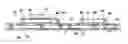
FIG. 2 is a cross-section view of a support 30 from which BGA packages are obtained. Support 30 has the shape of a wafer and comprises a central layer 35 formed of an insulating material. Metal tracks 36, 37 are arranged on opposite surfaces of central layer 35 and are covered respectively with insulating layers 38, 39. Metal vias 40 are formed in central layer 35, each via 40 connecting a metal track 36 arranged on a surface of central layer 35 to a metal track 37 arranged on the opposite surface of central layer 35.
FIG. 2 shows the structure obtained after attachment of electronic circuits 43, 44 to support 30. In FIG. 2, the two shown circuits 43, 44 are intended, at the end of the manufacturing process, to be on a same portion of support 30. However, at the present step of the manufacturing method, circuits 43, 44 are reproduced many times on support 30. As an example, circuit 43 is a transceiver circuit formed of a first integrated circuit chip 45 and of a second integrated circuit chip 46 attached to the first integrated circuit chip 45 according to a flip/chip-type connection and circuit 44 is a power amplifier circuit formed of an integrated circuit chip 47. The attachment of circuits 43, 44 to support 30 is obtained by depositing glue portions 48 on support 30, by laying circuits 43, 44 at the level of glue portions 48, and by polymerizing glue portions 48. The electric connections between circuits 43, 44 and support 30 are obtained via electric wires 49, for example, made of gold, connected to metal tracks 36 through insulating layer 38. It should be clear that the structures of circuits 43, 44 are given as an illustration only, where circuits 43, 44 may comprise a greater or smaller number of integrated circuit chips.
FIGS. 3 and 4 respectively are a cross-section view and a top view of a polysilicon wafer 50 on which a metal layer 52, for example, made of gold, aluminum, or silver, has been formed. As an example, the thickness of wafer 50 is on the order of 150 μm and the thickness of metal layer 52 is on the order of from 1 to 5 μm. Bumps 54, for example, made of tin, are distributed on metal layer 52. Bumps 54 may be formed by spreading welding paste on metal layer 52 through a mask to form welding paste pads, and by then melting the welding paste pads to give them a substantially spherical shape. To ease the positioning and the forming of bumps 54, metal layer 52 may be covered with an insulating layer, not shown, in which are formed openings at the level of the desired positions of bumps 54 to ease their forming. According to an alternative embodiment of the present invention, bumps 54 are replaced with pillar bumps having a substantially cylindrical shape, which may be formed of a cylindrical copper pad comprising a rounded tin end.
In top view, bumps 54 are distributed across wafer 50 according to a grid which delimits locations 56. As an example, bumps 54 have a diameter on the order of 800 μm. Bumps 54 may be separated, the distance separating two adjacent bumps 54 especially depending on the nature of the electromagnetic disturbances against which protection is desired. According to an alternative embodiment of the present invention, bumps 54 may be contiguous. According to another alternative embodiment of the present invention, some adjacent bumps 54 are at least partially in contact, while other adjacent bumps are separate.
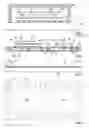
FIG. 5 is a cross-section view of the structure obtained after having sawn wafer 50 to form wafer portions 58, a single wafer portion 58 being shown in FIG. 5.
FIG. 6 is a cross-section view of the structure obtained after having attached to support 30 wafer portions 58 delimited at the preceding step, only one wafer portion 58 being shown in FIG. 5. Each wafer portion 58 may be attached to support 30 according to a flip-chip connection by properly orienting wafer portion 58 so that metal layer 52 faces support 30, circuits 43, 44 being above locations 56, and melting bumps 54 to attach wafer portion 58 to support 30. Openings are provided at the level of insulating layer 38 to expose metal portions 36 so that, for each wafer portion 58, bumps 54, or at least some of them, are in contact with the exposed metal tracks 36. Each circuit 43, 44 is then surrounded with bumps 54 and is above a portion of metal layer 52.
FIG. 7 shows the structure obtained after arrangement of an insulating material 59, for example, an epoxy resin and after having formed bumps 60, for example, tin, on the surface of support 30 opposite to circuits 43, 44. Some bumps 60 are connected to metal tracks 37 of support 30, through resin layer 39, enabling forming electric connections between bumps 60 and electric wires 49 and between bumps 60 and bumps 54. Insulating material 59 penetrates under wafer portion 58 and covers each circuit 43, 44. The interval between bumps 54 and the interval between circuits 43, 44 and wafer portion 58 must then be sufficient to enable a good penetration of the resin under wafer portion 58.
FIG. 8 shows the structure obtained after having sawn support 30 and insulating material 59 to define distinct electronic circuits 61, a single circuit 61 being shown in FIG. 8. Each electronic circuit 61 is formed, in the present example, of a portion 62 of support 30, forming a BGA package, to which are attached circuits 43 and 44, of wafer portion 58 covering circuits 43, 44, and of a resin block 64 surrounding wafer portion 58 and covering circuits 43, 44. The sawing of circuits 61 may be performed by means of a circular saw having a thickness that may be on the order of 100 micrometers. The dimensions of wafer portion 58 are advantageously smaller than the dimensions of the corresponding support portion 62 so that wafer portion 58 is not sawn as circuits 61 are delimited.
According to a variation of the present invention, the step in which insulating material 59 is arranged is not present. In this case, bumps 54 may be contiguous. It is then necessary for wafer portion 58 to have a sufficient thickness, for example, on the order of 300 μm, to ensure a sufficient mechanical protection of electronic circuits 43, 44 that it covers, which protection is otherwise partly ensured by resin block 64. Further, in this case, wafer portion 58 may come into contact with circuits 43, 44 or with one of them.
Electronic circuit 61 is, for example, intended to be attached to a motherboard. Bumps 54 and metal layer 52 may then be grounded via metal tracks 36 connected to bumps 54, and themselves connected to metal tracks 37 connected to bumps 60 which are, in turn, grounded via the motherboard. For each circuit 43, 44, the assembly formed by bumps 54 surrounding circuit 43, 44 and the portion of metal layer 52 opposite to circuit 43, 44 forms a metal cage 66, 68, which protects the circuit 43, 44 that it contains against external electromagnetic disturbances, especially electromagnetic disturbances transmitted by the other circuit 43, 44 attached to the same portion 62 of support 30.
Since the protection of circuits 43, 44 performed on the same portion 62 of support 30 is obtained by the corresponding metal cages 66, 68, it is then no longer necessary, when portion 62 of the support is subsequently attached to a motherboard, to provide a metal cover encapsulating support portion 62 which would anyway not protect each circuit 43, 44 against electromagnetic disturbances transmitted by the other circuit 43, 44 attached to the same support portion 62. For a circuit 61 of given dimensions, the provision of the protection device described above results in a smaller bulk than that resulting from the use of a metal cover. Indeed, the bulk of the protection device described above results from the addition of wafer portion 58, the thickness of which generally is on the order of 150 μm, to which adds the distance separating wafer portion 58 of circuits 43, 44 present when resin is injected under wafer portion 58, and which is on the order of 150 μm. When a distinct metal cover is used, it is necessary to provide an unoccupied region above circuit 61, generally greater than 1 mm to enable arrangement of the metal cover.
Further, the present invention enables proper setting of metal layer 52 and of bumps 54 to the motherboard ground. Indeed, some or even all of bumps 54 may be directly grounded via conductive tracks 36, enabling proper distribution of the voltages.
The present invention provides an electronic circuit protection circuit which, advantageously, results in few modifications with respect to a conventional electronic circuit manufacturing method. Indeed, the steps of forming wafer portions 58 implement conventional techniques of electronic circuit manufacturing methods.
Of course, the present invention is likely to have various alterations, modifications, and improvements which will readily occur to those skilled in the art. In particular, the present invention has been described for the protection of electronic circuits formed on a same BGA package. However, the present invention also relates to the protection of electronic circuits formed on a same LGA package and, more generally, to the protection of electronic circuits formed on a same support.
Such alterations, modifications, and improvements are intended to be part of this disclosure, and are intended to be within the spirit and the scope of the present invention. Accordingly, the foregoing description is by way of example only and is not intended to be limiting. The present invention is limited only as defined in the following claims and the equivalents thereto.
Claims
What is claimed is:1. A device for protecting an electronic circuit that includes a support to which are attached at least two circuit portions, each including at least one integrated circuit chip, comprising:
a wafer of a semiconductor material;
a conductive layer arranged parallel to the support and covering a surface of the wafer; and
conductive pillars connecting the wafer to the support, the conductive pillars being distributed around each circuit portion and in contact with the conductive layer.
2. The device of claim 1, wherein several adjacent conductive pillars are spaced apart, the device further comprising an insulating region arranged at least between the wafer and the support and covering each circuit portion.
3. The device of claim 1, wherein the support comprises:
a planar insulating portion;
first conductive tracks arranged on a first surface of the planar insulating portion, the first conductive tracks being connected to at least some of the conductive pillars;
second conductive tracks arranged on a second surface of the planar insulating portion opposite to the first surface, the second conductive tracks being for connection to a reference voltage; and
means, contained in the planar insulating portion, for connecting the first conductive tracks to the second conductive tracks.
4. The device of claim 1, wherein the conductive pillars have a spherical shape.
5. The device of claim 1, wherein the conductive pillars have an at least partly cylindrical shape.
6. The device of claim 1, wherein at least two adjacent conductive pillars are in contact.
7. The device of claim 1, wherein the support is a ball grid array package.
8. A method for manufacturing electronic circuits, comprising the steps of:
providing a planar support;
attaching on a surface of the support circuit portions, each containing at least one integrated circuit chip;
attaching, parallel to said surface of the support, wafer portions of a semiconductor material, each wafer portion covering at least two adjacent circuit portions, being covered with a metal layer on the side of said at least two adjacent circuit portions, and being connected to the support by conductive pillars distributed around each of said at least two adjacent circuit portions; and
delimiting electronic circuits, each comprising at least two adjacent circuit portions and the associated wafer portion.
9. The method of claim 8, wherein at least several adjacent conductive pillars are spaced apart and the delimiting step is preceded by introducing an insulating material between spaced apart portions of the conductive pillars and under each wafer portion to cover said at least two adjacent circuit portions.
10. The method of claim 8, wherein the wafer portions are obtained by sawing of a wafer on which the conductive pillars are distributed.
11. The method of claim 8 wherein the conductive pillars are formed by spreading welding paste through a mask on to the metal layer.
12. The method of claim 8 wherein the conductive pillars are formed by forming an insulating layer on the metal layer, etching the insulating layer to form openings, and forming the conductive pillars in the openings.
13. A protected electronic device, comprising:
a support;
first and second circuit portions positioned on the support, each circuit portion including at least one integrated circuit chip;
a wafer;
a conductive layer arranged parallel to the support and covering a surface of the wafer; and
conductive pillars connecting the wafer to the support, the conductive pillars being distributed around each circuit portion and in contact with the conductive layer.
14. The device of claim 13, wherein several adjacent conductive pillars are spaced apart, the device further comprising an insulating region arranged at least between the wafer and the support and covering each circuit portion.
15. The device of claim 13, wherein the support comprises:
a planar insulating portion;
first conductive tracks arranged on a first surface of the planar insulating portion, the first conductive tracks being connected to at least some of the conductive pillars;
second conductive tracks arranged on a second surface of the planar insulating portion opposite to the first surface, the second conductive tracks being for connection to a reference voltage; and
conductive vias extending through the planar insulating portion and connecting the first conductive tracks to the second conductive tracks.
16. The device of claim 13, wherein the conductive pillars have a spherical shape.
17. The device of claim 13, wherein the conductive pillars have an at least partly cylindrical shape.
18. The device of claim 13, wherein at least two adjacent conductive pillars are in contact.
19. The device of claim 13, wherein the conductive pillars are distributed around four sides of each of the circuit portions.
20. The device of claim 13 wherein the wafer is of semiconductor material.
Images & Drawings included:
Sources:
- United States Patent and Trademark Office - verify current appl. status at the USPTO↗
Similar patent applications:
- » 20230335921
ANTENNA DEVICE AND ELECTRONIC CIRCUIT PROTECTION DEVICE - » 20140293492
Protective circuit, electronic device, and method of driving a protective circuit - » 20250038525
ELECTRO-STATIC DISCHARGE (ESD) PROTECTION CIRCUIT AND ELECTRONIC DEVICE INCLUDING ESD PROTECTION CIRCUIT - » 20150138740
Integrated silicone for protecting electronic devices, circuit module using the same and manufacturing method of circuit module - » 10491134
Secondary lithium ion cell or battery, and protecting circuit, electronic device, and charging device of the same - » 20150043118
Input protection circuit, electronic device, electronic apparatus, and moving object - » 20160322811
Input protection circuit, electronic device, electronic apparatus, and moving object - » 20060023383
Electronic circuit protection device with It or other function - » 20060274517
Electronic circuit protection device - » 20100253292
SECONDARY LITHIUM ION CELL OR BATTERY, AND PROTECTING CIRCUIT, ELECTRONIC DEVICE AND CHARGING DEVICE OF THE SAME
Recent applications in this class:
- » 20250293178 2025-09-18
SEMICONDUCTOR DEVICE AND METHOD OF MANUFACTURING THEREOF - » 20250293177 2025-09-18
SYSTEMS AND METHODS FOR COMPONENT ISOLATION - » 20250293176 2025-09-18
SYSTEMS AND METHODS FOR COMPONENT ISOLATION - » 20250285991 2025-09-11
SYSTEM IN PACKAGE MODULE AND METHOD FOR FABRICATING THE SAME - » 20250285990 2025-09-11
SHIELDING PARTICLES COATED WITH ELECTRICAL INSULATION - » 20250273595 2025-08-28
Semiconductor Device and Method for Selective EMI Shielding Using a Mask - » 20250273594 2025-08-28
Semiconductor Device and Method of Forming Multi-Layer Shielding Structure Over the Semiconductor Device - » 20250273593 2025-08-28
Component Carrier With Cavity and Laser Protection Structure - » 20250273592 2025-08-28
PARTIALLY SHIELDED SEMICONDUCTOR DEVICE AND METHOD FOR FORMING THE SAME - » 20250273591 2025-08-28
ADDING SACRIFICIAL TRACES TO ABORB SIGNAL INTERFERENCE FROM HIGH SPEED AGGRESSOR TRACES
Recent applications for this Assignee:
- » 20240186090 2024-06-06
SWITCH BASED ON PHASE-CHANGE MATERIAL - » 20240178869 2024-05-30
RADIO FREQUENCY RECEIVER - » 20240118871 2024-04-11
Method, system, and circuit for generating toolchains agnostic linker scripts - » 20240072037 2024-02-29
PROTECTION AGAINST ELECTROSTATIC DISCHARGES - » 20240072036 2024-02-29
DEVICE OF PROTECTION AGAINST ELECTROSTATIC DISCHARGES - » 20240063290 2024-02-22
Bipolar transistor - » 20240023468 2024-01-18
SWITCH BASED ON PHASE-CHANGE MATERIAL - » 20240023465 2024-01-18
SWITCH BASED ON PHASE-CHANGE MATERIAL - » 20230393250 2023-12-07
TIME-OF-FLIGHT SENSOR AND METHOD FOR ADJUSTING AN EXPOSURE TIME OF SUCH A SENSOR - » 20230350593 2023-11-02
Method, system, and circuit for deploying file system on embedded memory in programmable computing device