Mounting and adhesive layer for semiconductor components
US20060292717A1
2006-12-28
11/450,902
2006-06-09
✅ Patent granted
US 7,582,909 B2
2009-09-01
-
-
Chris C Chu
2027-01-27
Abstract:
An assembly and adhesive layer for semiconductor components is arranged between a silicon support (submount) and an electronic functional element for the formation of an electrically-conducting connection between the silicon support and the functional element. The assembly and adhesive layer are arranged on the support. The assembly and adhesive layer are made from a Ti/TiN layer (6), applied to an aluminum contact surface (5) of the silicon support (1), by means of a deposition method. The aluminum contact surface (5) is located on a landing pad (2) on the silicon support (1).
Inventors:
- Werner Kuhlmann 3 🇩🇪 Muenchen, Germany
- Werner Kuhlmann 3 🇩🇪 Munich, Germany
- Benjamin Prodinger 2 🇦🇹 Wernberg, Austria
- Melanie Ring 1 🇩🇪 Muenchen, Germany
- Melanie Ring 2 🇩🇪 Munich, Germany
Assignee:
- Infineon Technologies AG 4,173 🇩🇪 Munich, Germany
Interested in similar patents?
Get notified when new applications in this technology area are published.
Classification:
H01L31/12 IPC
Semiconductor devices sensitive to infra-red radiation, light, electromagnetic radiation of shorter wavelength or corpuscular radiation and specially adapted either for the conversion of the energy of such radiation into electrical energy or for the control of electrical energy by such radiation; Processes or apparatus specially adapted for the manufacture or treatment thereof or of parts thereof; Details thereof structurally associated with, e.g. formed in or on a common substrate with, one or more electric light sources, e.g. electroluminescent light sources, and electrically or optically coupled thereto
H01L23/485 » CPC main
Details of semiconductor or other solid state devices; Arrangements for conducting electric current to or from the solid state body in operation, e.g. leads, terminal arrangements ; Selection of materials therefor consisting of lead-in layers inseparably applied to the semiconductor body consisting of layered constructions comprising conductive layers and insulating layers, e.g. planar contacts
H01L23/147 » CPC further
Details of semiconductor or other solid state devices; Mountings, e.g. non-detachable insulating substrates characterised by the material or its electrical properties Semiconductor insulating substrates
H01L24/33 » CPC further
Arrangements for connecting or disconnecting semiconductor or solid-state bodies; Methods or apparatus related thereto; Means for bonding being attached to, or being formed on, the surface to be connected, e.g. chip-to-package, die-attach, "first-level" interconnects; Manufacturing methods related thereto; Layer connectors, e.g. plate connectors, solder or adhesive layers; Manufacturing methods related thereto; Structure, shape, material or disposition of the layer connectors after the connecting process of a plurality of layer connectors
H01L24/83 » CPC further
Arrangements for connecting or disconnecting semiconductor or solid-state bodies; Methods or apparatus related thereto; Methods for connecting semiconductor or other solid state bodies using means for bonding being attached to, or being formed on, the surface to be connected using a layer connector
H01L24/45 » CPC further
Arrangements for connecting or disconnecting semiconductor or solid-state bodies; Methods or apparatus related thereto; Means for bonding being attached to, or being formed on, the surface to be connected, e.g. chip-to-package, die-attach, "first-level" interconnects; Manufacturing methods related thereto; Wire connectors; Manufacturing methods related thereto; Structure, shape, material or disposition of the wire connectors prior to the connecting process of an individual wire connector
H01L24/48 » CPC further
Arrangements for connecting or disconnecting semiconductor or solid-state bodies; Methods or apparatus related thereto; Means for bonding being attached to, or being formed on, the surface to be connected, e.g. chip-to-package, die-attach, "first-level" interconnects; Manufacturing methods related thereto; Wire connectors; Manufacturing methods related thereto; Structure, shape, material or disposition of the wire connectors after the connecting process of an individual wire connector
H01L33/62 » CPC further
Semiconductor devices with at least one potential-jump barrier or surface barrier specially adapted for light emission; Processes or apparatus specially adapted for the manufacture or treatment thereof or of parts thereof; Details thereof characterised by the semiconductor body packages Arrangements for conducting electric current to or from the semiconductor body, e.g. lead-frames, wire-bonds or solder balls
H01L2224/73265 » CPC further
Indexing scheme for arrangements for connecting or disconnecting semiconductor or solid-state bodies and methods related thereto as covered by; Means for bonding being of different types provided for in two or more of groups; Location after the connecting process on different surfaces Layer and wire connectors
H01L2224/83801 » CPC further
Indexing scheme for arrangements for connecting or disconnecting semiconductor or solid-state bodies and methods related thereto as covered by; Methods for connecting semiconductor or other solid state bodies using means for bonding being attached to, or being formed on, the surface to be connected using a layer connector; Bonding techniques Soldering or alloying
H01L2224/8389 » CPC further
Indexing scheme for arrangements for connecting or disconnecting semiconductor or solid-state bodies and methods related thereto as covered by; Methods for connecting semiconductor or other solid state bodies using means for bonding being attached to, or being formed on, the surface to be connected using a layer connector; Bonding techniques using an inorganic non metallic glass type adhesive, e.g. solder glass
H01L2924/01004 » CPC further
Indexing scheme for arrangements or methods for connecting or disconnecting semiconductor or solid-state bodies as covered by; Chemical elements Beryllium [Be]
H01L2924/01005 » CPC further
Indexing scheme for arrangements or methods for connecting or disconnecting semiconductor or solid-state bodies as covered by; Chemical elements Boron [B]
H01L2924/01006 » CPC further
Indexing scheme for arrangements or methods for connecting or disconnecting semiconductor or solid-state bodies as covered by; Chemical elements Carbon [C]
H01L2924/01013 » CPC further
Indexing scheme for arrangements or methods for connecting or disconnecting semiconductor or solid-state bodies as covered by; Chemical elements Aluminum [Al]
H01L2924/01019 » CPC further
Indexing scheme for arrangements or methods for connecting or disconnecting semiconductor or solid-state bodies as covered by; Chemical elements Potassium [K]
H01L2924/0102 » CPC further
Indexing scheme for arrangements or methods for connecting or disconnecting semiconductor or solid-state bodies as covered by; Chemical elements Calcium [Ca]
H01L2924/01024 » CPC further
Indexing scheme for arrangements or methods for connecting or disconnecting semiconductor or solid-state bodies as covered by; Chemical elements Chromium [Cr]
H01L2924/01027 » CPC further
Indexing scheme for arrangements or methods for connecting or disconnecting semiconductor or solid-state bodies as covered by; Chemical elements Cobalt [Co]
H01L2924/01032 » CPC further
Indexing scheme for arrangements or methods for connecting or disconnecting semiconductor or solid-state bodies as covered by; Chemical elements Germanium [Ge]
H01L2924/01046 » CPC further
Indexing scheme for arrangements or methods for connecting or disconnecting semiconductor or solid-state bodies as covered by; Chemical elements Palladium [Pd]
H01L2924/01047 » CPC further
Indexing scheme for arrangements or methods for connecting or disconnecting semiconductor or solid-state bodies as covered by; Chemical elements Silver [Ag]
H01L2924/01049 » CPC further
Indexing scheme for arrangements or methods for connecting or disconnecting semiconductor or solid-state bodies as covered by; Chemical elements Indium [In]
H01L2924/0105 » CPC further
Indexing scheme for arrangements or methods for connecting or disconnecting semiconductor or solid-state bodies as covered by; Chemical elements Tin [Sn]
H01L2924/01078 » CPC further
Indexing scheme for arrangements or methods for connecting or disconnecting semiconductor or solid-state bodies as covered by; Chemical elements Platinum [Pt]
H01L2924/01079 » CPC further
Indexing scheme for arrangements or methods for connecting or disconnecting semiconductor or solid-state bodies as covered by; Chemical elements Gold [Au]
H01L2924/01082 » CPC further
Indexing scheme for arrangements or methods for connecting or disconnecting semiconductor or solid-state bodies as covered by; Chemical elements Lead [Pb]
H01L2924/014 » CPC further
Indexing scheme for arrangements or methods for connecting or disconnecting semiconductor or solid-state bodies as covered by; Alloys Solder alloys
H01L2924/04941 » CPC further
Indexing scheme for arrangements or methods for connecting or disconnecting semiconductor or solid-state bodies as covered by; Nitrides composed of metals from groups of the periodic table 4th Group TiN
H01L2924/07811 » CPC further
Indexing scheme for arrangements or methods for connecting or disconnecting semiconductor or solid-state bodies as covered by; Polymers; Adhesive characteristics other than chemical being an ohmic electrical conductor Extrinsic, i.e. with electrical conductive fillers
H01L2924/12041 » CPC further
Indexing scheme for arrangements or methods for connecting or disconnecting semiconductor or solid-state bodies as covered by; Details of semiconductor or other solid state devices to be connected; Device type; Passive devices, e.g. 2 terminal devices; Optical Diode LED
H01L2924/3025 » CPC further
Indexing scheme for arrangements or methods for connecting or disconnecting semiconductor or solid-state bodies as covered by; Technical effects; Electrical effects Electromagnetic shielding
H01L2924/0665 » CPC further
Indexing scheme for arrangements or methods for connecting or disconnecting semiconductor or solid-state bodies as covered by; Polymers Epoxy resin
H01L2924/12043 » CPC further
Indexing scheme for arrangements or methods for connecting or disconnecting semiconductor or solid-state bodies as covered by; Details of semiconductor or other solid state devices to be connected; Device type; Passive devices, e.g. 2 terminal devices; Optical Diode Photo diode
H01L2924/00 » CPC further
Indexing scheme for arrangements or methods for connecting or disconnecting semiconductor or solid-state bodies as covered by
H01L2924/00014 » CPC further
Indexing scheme for arrangements or methods for connecting or disconnecting semiconductor or solid-state bodies as covered by; Technical content checked by a classifier the subject-matter covered by the group, the symbol of which is combined with the symbol of this group, being disclosed without further technical details
H01L2924/207 » CPC further
Indexing scheme for arrangements or methods for connecting or disconnecting semiconductor or solid-state bodies as covered by; Parameters Diameter ranges
H01L21/00 IPC
Processes or apparatus adapted for the manufacture or treatment of semiconductor or solid state devices or of parts thereof
H01L27/15 IPC
Devices consisting of a plurality of semiconductor or other solid-state components formed in or on a common substrate including semiconductor components with at least one potential-jump barrier or surface barrier specially adapted for light emission
H01L33/00 IPC
Semiconductor devices with at least one potential-jump barrier or surface barrier specially adapted for light emission; Processes or apparatus specially adapted for the manufacture or treatment thereof or of parts thereof; Details thereof
Description
This application is a continuation of co-pending International Application No. PCT/DE2004/002701, filed Dec. 8, 2004, which designated the United States and was not published in English, and which is based on German Application No. 103 57 673.8 filed Dec. 9, 2003, both of which applications are incorporated herein by reference.
TECHNICAL FIELDThe invention relates to a mounting and adhesive layer for semiconductor components between a silicon carrier and an electronic functional element for forming an electrically conducting connection between the silicon carrier and the functional element.
BACKGROUNDIn addition to conventional soldering using a lead-containing solder, electrically conductive adhesive bonding is increasingly being used to produce electrical connections between silicon components and carrier elements in the field of microelectronics. The main reason for this is the ban of the use of lead for soldering purposes decreed by the European Union. For this reason, it is necessary to use lead-free solders to produce electrical connections. However, the drawback of lead-free solders lies in the considerably higher melting temperature (170-185° C.).
For applications that require a low-heat joining process at temperatures up to at most approx. 85° C., electrically conductive adhesive bonding is the preferred connection technology.
In one specific example, an LED (light emitting diode) is to be mounted on a silicon carrier (submount). This requires the LED to be mounted on the surface of the silicon carrier and, at the same time, to be electrically contact-connected. To achieve this, the rear side contact of the LED has to be connected to the submount surface via a conducting connection. The second contact required is then contact-connected to the submount surface from the top side of the LED via a bonding wire. This connection can be produced with the aid of standard wire bonding techniques. For this purpose, aluminum contact surfaces are usually provided on the submount in order to allow contact-connection of the bonding wire, which may consist of aluminum.
However, on account of the inevitable formation of an oxide layer on the metal surface, the metallization (Al) used here is not suitable for electrically conductive adhesive bonding. The oxide layer (insulator), which is present on the metal surface, is formed in the case of components that are not hermetically packaged unless measures are taken to avoid this. This oxide layer forms because the epoxy resin adhesive that is customarily used is relatively pervious to moisture.
In order nevertheless to be able to realize an electrically conductive connection, an adhesive and conductive connection is required on what is known as the chip land surface.
Precious metals, such as silver, platinum, palladium, etc., have proven to be materials that can be used for this purpose, since they scarcely form an oxide layer or, in the case of silver, form a conducting oxide layer. However, on account of the electrochemical series, in conjunction with catalysts (e.g., moisture), aluminum pitting (corrosion) can occur.
Another possible option is to use ITO (indium tin oxide). A layer of this material is frequently used in semiconductor fabrication and in LCDs (liquid crystal displays) since it is both transparent and conductive. Therefore, this layer can be used as a light-transmitting electrode for LEDs (light emitting diodes) and also for LCDs. It can also be used as an opaque screening means, for example, above the photodiode of an optocoupler in order to increase the common-mode rejection or in very general terms to improve the sensitivity to interfering electromagnetic radiation.
If an ITO layer of this type is to be bonded to a standard aluminum metallization, the problem arises that the oxygen of the ITO layer oxidizes the uppermost Al layer, with the result that the inherently conductive connection is interrupted. To avoid this, a precious metal is recommended as an interface, in which context platinum can be used together with Ti or Cr as an adhesion promoter.
There are usually two ways of realizing a bondable and adhesive metallization. The first known way is a base metallization for bonding (e.g., Al) and a further precious metal metallization or a metal that is less prone to oxidation (e.g., TiPt), which is applied only in the region of the adhesive surface. The second way consists in a precious metal metallization, which is both adhesive and bondable (e.g., TiPtAu).
The first way has the drawback that corrosion can occur between the two metallizations via the intervention of a catalyst. The second way has the particular disadvantage that on account of the extremely low surface roughness of Au, bonding problems can occur with further layers or, for example, with potting resins. Furthermore, TiPtAu is available in very few silicon lines, and, consequently, additional investment costs would be incurred, whereas Al is a standard metallization for silicon.
SUMMARY OF THE INVENTIONThe invention is now based on the object of providing a mounting and adhesive layer for semiconductor components for producing electrical connections to carrier elements, which can be produced in a particularly simple way and reliably avoids the build-up of electrochemical stresses.
The object on which the invention is based is achieved by virtue of the fact that the mounting and adhesive layer includes a Ti/Ti-nitride layer and is applied by a deposition process to an aluminum contact surface of the silicon carrier, the aluminum contact surface being located on a landing pad of the silicon carrier.
The Ti/Ti-nitride layer may in this case be applied to the entire contact surface of the carrier or at least to the landing pad.
Standard deposition processes, such as PCVD processes or sputtering, are suitable for the deposition of the Ti/TiN layer.
Particular advantages of using Ti/TiN as a mounting and adhesive surface are the known process and deposition properties in semiconductor fabrication. A further advantage is that a build-up of electrochemical stresses, as may occur with different metallizations, leading to corrosion, is avoided. Furthermore, the Ti/TiN layer has good adhesive properties, a suitable surface condition and a low contact resistance with respect to other metals, and also bonds well to oxides and nitrides. Furthermore, titanium nitride is available as a standard material in CMOS fabrication, where it is often used as a diffusion barrier between silicon and aluminum.
DESCRIPTION OF THE DRAWINGSThe invention is to be explained in more detail below on the basis of an exemplary embodiment. In the associated drawings:
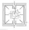
FIG. 1 diagrammatically depicts a LED mounted on a silicon carrier; and
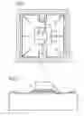
FIG. 2 shows a side view of the arrangement from FIG. 1.
The following list of reference symbols can be used in conjunction with the figures:
- 1. Silicon carrier
- 2. Landing pad
- 3. LED
- 4. Conductive adhesive
- 5. Aluminum contact surface
- 6. Ti/Ti-nitride layer
- 7. Interconnect
- 8. Contact pad
- 9. Contact pad
- 10. Bonding wire
- 11. Front side contact
FIGS. 1 and 2 show a silicon carrier 1 (submount) with a central landing pad 2 made from silicon, on which an LED 3 has been mounted via a conductive adhesive bond with the aid of a conductive adhesive 4.
An aluminum contact surface 5 has been applied to the landing pad 2, for example by means of a PVD process, to produce the electrical contact between the landing pad 2 and the rear side electrode (not shown) of the LED 3. Since aluminum, as has already been explained, under appropriate ambient conditions, forms a non-conducting aluminum oxide layer on the surface, a Ti/Ti-nitride layer 6 is deposited immediately after the deposition of Al.
The Ti/TiN layer 6 reliably protects the aluminum contact surface 5 from oxidation, so that a permanently low contact resistance of the contact between the rear side electrode of the LED 3 and the landing pad 2 on the silicon carrier 1, comprising the aluminum contact surface 5, the Ti/TiN layer 6 and the conductive adhesive 4, is ensured.
To allow the arrangement described to be electrically connected to other modules, the landing pad 2 is connected to a contact pad 8 via an interconnect 7. Finally, there is also a further contact pad 9, which is connected to the front side contact 11 of the LED 3 via a bonding wire 10 (wire bridge).
It will be understood that this embodiment constitutes just one example of numerous possible embodiments of the invention.
Claims
What is claimed is:1. A mounting and adhesive layer for semiconductor components between a silicon carrier and an electronic functional element for forming an electrically conducting connection between the silicon carrier and the functional element, the mounting and adhesive layer being located on the carrier, wherein the mounting and adhesive layer consists of a Ti/Ti-nitride layer and is applied by a deposition process to an aluminum contact surface of the silicon carrier, the aluminum contact surface being located on a landing pad of the silicon carrier.
2. The mounting and adhesive layer as claimed in claim 1, wherein the Ti/Ti-nitride layer is applied to an entire contact surface of the silicon carrier.
3. The mounting and adhesive layer as claimed in claim 1, wherein the Ti/Ti-nitride layer is applied at least to the landing pad.
4. The mounting and adhesive layer as claimed in claim 1, wherein the Ti/Ti-nitride layer is applied by a PCVD process.
5. The mounting and adhesive layer as claimed in claim 1, wherein the Ti/Ti-nitride layer is applied by sputtering.
6. A method of mounting a light emitting diode (LED) on a silicon submount, the method comprising:
providing a silicon submount with a landing pad;
providing the landing pad with an aluminum contact area;
coating the aluminum on the contact area with a protective Ti/TiN layer;
depositing an electrically conductive adhesive on the Ti/TiN layer;
adhering a backside electrode of an LED on the conductive adhesive; and
connecting a front side contact of the LED with a contact pad on the silicon submount by wire bonding.
7. The method according to claim 6, wherein the Ti/TiN layer is deposited on the entire contact area.
8. The method according to claim 6, wherein the Ti/TiN layer is deposited at least on the landing pad.
9. The method according to claim 6, wherein the Ti/TiN layer is deposited by a PCVD process.
10. The method according to claim 6, wherein the Ti/TiN layer is deposited by a sputtering process.
11. The method according to claim 6, wherein the aluminum contact area comprises pure aluminum.
12. The method according to claim 6, wherein providing the landing pad comprises depositing aluminum using a physical vapor deposition process.
13. An electrical component comprising:
a carrier having a first contact and a second contact;
an aluminum contact surface electrically connected to the first contact;
a Ti/TiN layer overlying the aluminum contact surface; and
an electronic functional element comprising a first electrode and a second electrode, wherein the first electrode is electrically connected to the Ti/TiN layer and mechanically connected to the carrier by an electrically conductive adhesive and wherein the second electrode is wire bonded to the second contact.
14. The electrical component according to claim 13, wherein the electronic functional element comprises a light emitting diode (LED).
15. The electrical component according to claim 14, wherein the first electrode is disposed on a first surface of the LED and the second electrode is disposed on a second surface of the LED, the first surface opposed from the second surface.
16. The electrical component according to claim 13, wherein the aluminum contact surface comprises a pure aluminum.
17. The electrical component according to claim 13, wherein Ti is in direct contact with the aluminum contact surface and TiN is in direct contact with the electrically conductive adhesive.
18. The electrical component according to claim 13, wherein the carrier comprises a silicon carrier.
19. The electrical component according to claim 13, wherein the Ti/TiN layer overlies an entire surface of the aluminum contact surface.
20. The electrical component according to claim 13, wherein the Ti/TiN layer overlies only a portion of the aluminum contact surface.
Images & Drawings included:
Sources:
- United States Patent and Trademark Office - verify current appl. status at the USPTO↗
Recent applications in this class:
- » 20250157891 2025-05-15
BURIED METAL LINER IN SOURCE/DRAIN EPITAXIAL MATERIAL - » 20250118633 2025-04-10
SEMICONDUCTOR ARRANGEMENT COMPRISING A SEMICONDUCTOR ELEMENT WITH AT LEAST ONE CONNECTION ELEMENT - » 20250029897 2025-01-23
SEMICONDUCTOR DEVICE - » 20240421041 2024-12-19
LEADFRAME-LESS LASER DIRECT STRUCTURING (LDS) PACKAGE - » 20240304524 2024-09-12
SEMICONDUCTOR DEVICE - » 20240250004 2024-07-25
METHOD FOR FABRICATING A SEMICONDUCTOR DEVICE INCLUDING AN EMBEDDED SEMICONDUCTOR DIE - » 20240213122 2024-06-27
SEMICONDUCTOR DEVICE AND METHOD OF MANUFACTURING SEMICONDUCTOR DEVICE - » 20240153851 2024-05-09
SEMICONDUCTOR DEVICE - » 20240021501 2024-01-18
CONTACT PLUGS FOR SEMICONDUCTOR DEVICE AND METHOD OF FORMING SAME - » 20230352371 2023-11-02
SEMICONDUCTOR DEVICE
Recent applications for this Assignee:
- » 20190222018 2019-07-18
Temperature sensing and fault detection for paralleled double-side cooled power modules - » 20190120879 2019-04-25
Readout circuit for resistive and capacitive sensors - » 20170125556 2017-05-04
Tunnel field effect transistors - » 20160072383 2016-03-10
System and method for a controlled feedback charge pump - » 20160064451 2016-03-03
Semiconductor component comprising magnetic field sensor - » 20150137309 2015-05-21
Methods of fabricating isolation regions of semiconductor devices and structures thereof - » 20120278520 2012-11-01
System and method of transmitting data between devices connected via a bus defining a time slot during transmission for responsive output information from bus devices - » 20120199909 2012-08-09
Semiconductor devices and methods of manufacture thereof - » 20120162924 2012-06-28
Integrated Semiconductor Outline Package - » 20120081105 2012-04-05
Signal generation for spectral measurements