Method for producing means of connecting and/or soldering a component
US20070049065A1
2007-03-01
11/503,856
2006-08-14
✅ Patent granted
US 7,509,733 B2
2009-03-31
-
-
C. J Arbes
2026-11-09
Abstract:
A method for producing a mechanism for connecting and/or soldering or sealing a component on a substrate, including depositing on the substrate a layer made of a ductile material which, if applicable, conducts electricity, and stamping the layer thus produced by means of an etched die, the etching depending on the shape that one wishes to give the mechanism for connecting and/or soldering.
Inventors:
- François MARION 27 🇫🇷 Saint-Martin Le Vinoux, France
- Francçis Marion 1 🇫🇷 Saint Martin le Vinoux, France
Assignee:
- Commissariat A L'Energie Atomique 1,591 🇫🇷 Paris, France
Interested in similar patents?
Get notified when new applications in this technology area are published.
Classification:
B81C1/00269 » CPC main
Manufacture or treatment of devices or systems in or on a substrate for manufacturing microsystems; Processes for packaging MEMS devices Bonding of solid lids or wafers to the substrate
H01L24/11 » CPC further
Arrangements for connecting or disconnecting semiconductor or solid-state bodies; Methods or apparatus related thereto; Means for bonding being attached to, or being formed on, the surface to be connected, e.g. chip-to-package, die-attach, "first-level" interconnects; Manufacturing methods related thereto; Bump connectors ; Manufacturing methods related thereto Manufacturing methods
H05K3/3478 » CPC further
Apparatus or processes for manufacturing printed circuits; Assembling printed circuits with electric components, e.g. with resistor electrically connecting electric components or wires to printed circuits by soldering; Solder materials or compositions; Methods of application thereof Applying solder preforms; Transferring prefabricated solder patterns
B81C2201/0153 » CPC further
Manufacture or treatment of microstructural devices or systems in or on a substrate; Shaping material; Structuring the bulk substrate or layers on the substrate; Film patterning; Film patterning; Imprinting Imprinting techniques not provided for in
B81C2203/019 » CPC further
Forming microstructural systems; Packaging MEMS; Seals characterised by the material or arrangement of seals between parts
H01L24/13 » CPC further
Arrangements for connecting or disconnecting semiconductor or solid-state bodies; Methods or apparatus related thereto; Means for bonding being attached to, or being formed on, the surface to be connected, e.g. chip-to-package, die-attach, "first-level" interconnects; Manufacturing methods related thereto; Bump connectors ; Manufacturing methods related thereto; Structure, shape, material or disposition of the bump connectors prior to the connecting process of an individual bump connector
H01L2224/05001 » CPC further
Indexing scheme for arrangements for connecting or disconnecting semiconductor or solid-state bodies and methods related thereto as covered by; Means for bonding being attached to, or being formed on, the surface to be connected, e.g. chip-to-package, die-attach, "first-level" interconnects; Manufacturing methods related thereto; Bonding areas; Manufacturing methods related thereto; Structure, shape, material or disposition of the bonding areas prior to the connecting process of an individual bonding area Internal layers
H01L2224/11001 » CPC further
Indexing scheme for arrangements for connecting or disconnecting semiconductor or solid-state bodies and methods related thereto as covered by; Means for bonding being attached to, or being formed on, the surface to be connected, e.g. chip-to-package, die-attach, "first-level" interconnects; Manufacturing methods related thereto; Bump connectors; Manufacturing methods related thereto; Manufacturing methods Involving a temporary auxiliary member not forming part of the manufacturing apparatus, e.g. removable or sacrificial coating, film or substrate
H01L2224/11602 » CPC further
Indexing scheme for arrangements for connecting or disconnecting semiconductor or solid-state bodies and methods related thereto as covered by; Means for bonding being attached to, or being formed on, the surface to be connected, e.g. chip-to-package, die-attach, "first-level" interconnects; Manufacturing methods related thereto; Bump connectors; Manufacturing methods related thereto; Manufacturing methods by patterning a pre-deposited material Mechanical treatment, e.g. polishing, grinding
H05K3/062 » CPC further
Apparatus or processes for manufacturing printed circuits in which the conductive material is applied to the surface of the insulating support and is thereafter removed from such areas of the surface which are not intended for current conducting or shielding the conductive material being removed chemically or electrolytically, e.g. by photo-etch process; Etching masks consisting of metals or alloys or metallic inorganic compounds
H05K2203/0113 » CPC further
Indexing scheme relating to apparatus or processes for manufacturing printed circuits covered by; Tools for processing; Objects used during processing for patterning or coating Female die used for patterning or transferring, e.g. temporary substrate having recessed pattern
H05K2203/0405 » CPC further
Indexing scheme relating to apparatus or processes for manufacturing printed circuits covered by; Soldering or other types of metallurgic bonding Solder foil, tape or wire
H05K2203/0405 » CPC further
Indexing scheme relating to apparatus or processes for manufacturing printed circuits covered by; Soldering or other types of metallurgic bonding Solder foil, tape or wire
H05K2203/043 » CPC further
Indexing scheme relating to apparatus or processes for manufacturing printed circuits covered by; Soldering or other types of metallurgic bonding Reflowing of solder coated conductors, not during connection of components, e.g. reflowing solder paste
H05K2203/043 » CPC further
Indexing scheme relating to apparatus or processes for manufacturing printed circuits covered by; Soldering or other types of metallurgic bonding Reflowing of solder coated conductors, not during connection of components, e.g. reflowing solder paste
Y10T29/49155 » CPC further
Metal working; Method of mechanical manufacture; Electrical device making; Conductor or circuit manufacturing; On flat or curved insulated base, e.g., printed circuit, etc. Manufacturing circuit on or in base
Y10T29/49158 » CPC further
Metal working; Method of mechanical manufacture; Electrical device making; Conductor or circuit manufacturing; On flat or curved insulated base, e.g., printed circuit, etc.; Manufacturing circuit on or in base with molding of insulated base
H01L2924/15787 » CPC further
Indexing scheme for arrangements or methods for connecting or disconnecting semiconductor or solid-state bodies as covered by; Details of package parts other than the semiconductor or other solid state devices to be connected; Die mounting substrate; Material with a principal constituent of the material being a non metallic, non metalloid inorganic material Ceramics, e.g. crystalline carbides, nitrides or oxides
H01L2924/14 » CPC further
Indexing scheme for arrangements or methods for connecting or disconnecting semiconductor or solid-state bodies as covered by; Details of semiconductor or other solid state devices to be connected; Device type Integrated circuits
H01L2924/00 » CPC further
Indexing scheme for arrangements or methods for connecting or disconnecting semiconductor or solid-state bodies as covered by
H01L2224/114 » CPC further
Indexing scheme for arrangements for connecting or disconnecting semiconductor or solid-state bodies and methods related thereto as covered by; Means for bonding being attached to, or being formed on, the surface to be connected, e.g. chip-to-package, die-attach, "first-level" interconnects; Manufacturing methods related thereto; Bump connectors; Manufacturing methods related thereto; Manufacturing methods by blanket deposition of the material of the bump connector
H01L2924/00014 » CPC further
Indexing scheme for arrangements or methods for connecting or disconnecting semiconductor or solid-state bodies as covered by; Technical content checked by a classifier the subject-matter covered by the group, the symbol of which is combined with the symbol of this group, being disclosed without further technical details
H05K1/00 IPC
Printed circuits
H05K1/00 IPC
Printed circuits
H05K3/02 IPC
Apparatus or processes for manufacturing printed circuits in which the conductive material is applied to the surface of the insulating support and is thereafter removed from such areas of the surface which are not intended for current conducting or shielding
H05K3/02 IPC
Apparatus or processes for manufacturing printed circuits in which the conductive material is applied to the surface of the insulating support and is thereafter removed from such areas of the surface which are not intended for current conducting or shielding
H01L21/44 IPC
Processes or apparatus adapted for the manufacture or treatment of semiconductor or solid state devices or of parts thereof; Manufacture or treatment of semiconductor devices or of parts thereof the devices having at least one potential-jump barrier or surface barrier, e.g. PN junction, depletion layer or carrier concentration layer the devices having semiconductor bodies not provided for in groups, , , and with or without impurities, e.g. doping materials Manufacture of electrodes on semiconductor bodies using processes or apparatus not provided for in groups -
Description
SUMMARY OF THE INVENTIONThe present invention relates to the field of microelectronics, more specifically to the field of hybridisation and soldering or sealing techniques using fusible solder materials.
DESCRIPTION OF THE PRIOR ARTDevelopments in integrated-circuit technology have made it possible to achieve a high degree of miniaturisation and, in particular, the fabrication of microcomponents.
Hybridising chips on multilayer substrates in order to obtain interconnections between chips by means of conducting solder bumps is one of the technical achievements that has made such miniaturisation possible. This technology, better known as “flip-chip” technology, makes it possible to hybridise hundreds of chips on ceramic substrates.
It uses conducting microbumps that are generally made of a material that has a low melting point, such as SnPb, In or AgCuSn, and this technology has now been largely mastered.
In the same field, but in a different application, a number of these microcomponents are encapsulated inside a package or protective cover or equivalent type structure, thus making it possible to ensure protection again shock, corrosion, stray electromagnetic radiation, etc.
In addition, such protective packages or covers also make it possible for such microcomponents to operate in a vacuum or in a controlled atmosphere (pressure, inert gas, etc.) or after leaktight sealing from their ambient atmosphere.
Such a package or cover is classically sealed by means of a joint or sealing seam applied around the periphery of the component in question, generally on a wettable area or surface which is also referred to as an adhesion surface.
More frequently, fabrication of the components in question, regardless whether they are microsensors, microactuators, micro-electro-mechanical systems (MEMS), etc., therefore requires the use of solder and/or connection elements having different heights measured in relation to a coordinate system consisting of the upper surface of the substrate on which the microcomponents in question are placed or mounted.
There are currently several known technologies that make it possible to produce such solder seams or deposit bumps or microbumps for hybridising and therefore connecting.
The following techniques deserve mention:
-
- evaporation through a mask and soldering;
- “solder jetting”, a jet of droplets of solder similar to the droplets of ink used in inkjet printers;
- electrolysis;
- screen printing.
However, all these techniques always involve at least two operations in order to obtain solder and connection elements having different heights.
In addition, most of these technologies are expensive to implement, in particular because of the manipulations that they require.
The object of the present invention is precisely to dispense with the use of two consecutive stages in order to produce solder elements of different heights and, consequently, to reduce fabrication costs.
SUMMARY OF THE INVENTIONThe present invention refers to a method for producing means of connecting and/or soldering or sealing a component on a substrate.
This method involves:
-
- depositing on said substrate a layer of ductile material which, if applicable, conducts electricity;
- stamping the layer thus produced by means of an etched die, the etching depending on the shape that one wishes to give said means of connecting and/or soldering.
In other words, the invention involves, during the fabrication process, carrying out no more and no less than one process to mould a material that is sufficiently ductile to enable it to deform, especially at ambient temperature, in similar fashion to widely-known technologies used to mint coins, or doing so at a temperature that is close to the melting temperature of said material or even a temperature above the latter.
In fact, it is necessary to give the stamping or punching die the desired shapes, especially the various depths desired, in order to obtain differing heights of the means of soldering or connecting.
Obviously, the height of the layer of ductile material previously deposited is adequate to allow correct stamping by the die and, consequently, the realisation of different materials heights.
According to one aspect of the invention, the layer of ductile material is deposited on the wettable surfaces or areas previously produced on the substrate that accommodates the component or microcomponent. These wettable areas or surfaces are typically made of gold after producing a barrier layer that is typically made of nickel.
According to a first embodiment of the invention, these wettable areas or surfaces are precisely made depending on the desired profile of the means of soldering or connecting, i.e. they occupy a surface on the corresponding substrate that substantially matches the surface occupied on the same substrate by the connection and/or solder elements produced by the method according to the invention.
According to another embodiment of the invention, these wettable areas or surfaces cover the entire substrate and the layer intended to constitute these wettable surfaces is removed from the substrate between those areas accommodating the ductile material by etching after depositing said layer of ductile material, the latter acting as a mask during the operation to etch the layer that constitutes the wettable surfaces.
Finally and according to the invention, the ductile material is given a shape, after formatting or punching, that corresponds to the desired shape by remelting at a temperature in excess of the melting temperature of the ductile material.
Adopting this approach, in particular, produces a bump shape or if one wishes to have a sealing seam one gives the layer of ductile material thus deposited an overall cylindrical shape.
BRIEF DESCRIPTION OF THE DRAWINGSThe way in which the invention is implemented and its resulting advantages will be made more readily understandable by the descriptions of the following embodiments, given merely by way of example, reference being made to the accompanying drawings.
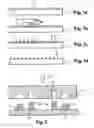
FIGS. 1a to 1d are schematic views of the principle used by the present invention.
FIG. 2 is a schematic cross-sectional view intended to illustrate the process of stamping the ductile material according to a first embodiment.
FIGS. 3a and 3b are views similar to FIG. 2, but of another embodiment.
FIGS. 4a to 4e are, respectively, a schematic top view (FIG. 4a) and cross-sectional views (FIGS. 4b to 4d) of use of the method according to the invention in order to make bumps on a CMOS wafer.
DESCRIPTION OF THE PREFERRED EMBODIMENTSFIGS 1a to 1d schematically illustrate the general principle underlying the method in accordance with the invention.
According to this principle, the substrate 1 is typically made of silicon. This substrate consists, for example, of a wafer measuring 300 mm for instance.
One then deposits or transfers a layer of solder material 2 onto the wafer. This material is ductile and typically consists of indium or a tin-lead alloy or an AgCuSn alloy.
A stamping process is then performed (FIG 1b) by means of a die 3 with punches 4 or having shapes 7, 8 made in it that together define punches 4 (see FIG. 2 and FIG. 3a).
This die operates on the step-and-repeat principle: in this case the die is the same size as one photo composition field; it is applied to each field and the step-and-repeat process is based on the field pitch.
However, this die can also operate on an entire wafer in a global fashion: the die is then the same size as the wafer 1 and the stamping operation is performed in a single pass.
The die 3 is actuated by an automatic or manual press so that it stamps said layer of ductile material 2 in the direction shown by arrow 5.
To achieve this, the lower wall of shapes 7, 8 and the lower surface of the die are coated with a non-stick coating made of polytetrafluoroethylene (PTFE) for example and said die is then applied to the surface of the layer of ductile material 2 that is to be stamped with a pressure P 4. The die is then backed off, thus defining a succession of shapes depending on shapes 7 and 8 of said die.
This die is advantageously made of silicon. In fact, it has been found that using such a material makes it possible to achieve extremely fine patterns thereby making it possible to produce moulds using conventional photolithography and chemical etching at low cost and, in particular, makes it possible to produce patterns that have a natural trapezoidal shape, thereby encouraging stripping.
After stripping, some recessed areas are likely to contain solder residues that are removed by etching.
Finally (FIG. 1d), the bumps are formed using the conventional technique of remelting solder elements, i.e. by increasing the temperature to a temperature in excess of the melting temperature of said ductile material.
The bump shape is produced thanks to the natural phenomenon of decrease in surface tension and if a solder seam is used, remelting produces a substantially circular cross-section.
Nevertheless, most of the time the solder elements, whether they are sealing seams or conductive sealing bumps or microbumps, are transferred onto a wettable surface or area.
To achieve this, prior to depositing the layer of solder 2, a barrier layer of nickel is produced, especially using an electroless method, on the open pads following foundry operations that result in the production of the silicon CMOS wafer.
A layer of gold (gold acting as the adhesion metal and hence wettable surface) is transferred onto this nickel barrier layer using known processes such as that developed, for instance, by the company PACTECH.
According to the invention, there are two possible alternatives. The first alternative is to produce this double nickel/gold layer only in those locations where solder elements are ultimately located, regardless whether these are seams or microbumps (FIG. 2).
In this case, the wettable areas are pre-etched and the operation to deposit and format or punch the layer of ductile material 2 intended to constitute solder or connection elements takes place as defined above.
In another embodiment shown in FIGS. 3a and 3b, the entire upper surface of the wafer, except the surface intended to accommodate the component or microcomponent obviously, is coated in the nickel/gold layer 10. In this case, after the layer of ductile material 2 has been stamped to obtain the desired shape, the double barrier layer of nickel/gold is removed from areas that do not have solder elements by etching.
In both cases, it is possible that there will still be a film of ductile material between the shapes produced after stamping. An etching process must then be performed in order to remove this residue. To achieve this, the entire surface is refreshed by etching a fine layer of ductile material, both on the shapes and between the shapes.
In the second embodiment, this etching is followed by a second etching that removes the barrier layer between the shapes.
A more precise embodiment of the invention will now be described, reference being made to FIG. 4. This embodiment uses a CMOS wafer 15 from the silicon foundry measuring 300 mm by 300 mm. This has a certain number of conductive aluminium pads 16 that are spaced 100 μm apart and distributed around the periphery of the wafer. The surface area of the chip is 1 cm2 and the height of the pads is 50 μm.
Thus, for a chip having a side length of 1 cm (surface area=108 μm2), one deposits an 1.8 μm thick layer of indium. This gives a volume of ductile material equal to 1.8. 108 μm3. This chip is then stamped by a die etched to obtain 1000 pads measuring 60×60 μm. The solder practically covers the pads completely, the latter have a height of approximately 50 μm.
The real attractiveness of the method according to the invention is readily apparent to the extent that, in a single operation, it makes it possible to obtain solder elements of different size, something which was previously not possible. In addition, the techniques used, especially direct punching, but also electrolytic evaporation, make it possible to keep the cost price of such components down.
This being so, it is feasible to fabricate active microcomponents, especially electronic components, using this method, especially arrays for detecting electromagnetic radiation and, more especially, infrared radiation, regardless whether or not they incorporate compensation for the expansion that is inherent in changes in operating temperature.
It is also possible to produce sealing seams concomitantly with connection bumps for hermetic seals, especially to use a protective cover or packaging in order to hermetically seal the component.
Finally, the invention is also applicable to the preparation of hybridisation bumps and, generally speaking, to producing all hybridised components regardless whether they are components that operate in the optical or x-ray spectrum or to hybridisation on flexible tape, on ceramics, on a multi-chip module or on a board: “chip on board” (COB) (printed circuit) or on glass “chip on glass” (COG).
Claims
1. A method for producing means of connecting and/or soldering or sealing a component on a substrate 1, characterised in that it involves:
depositing on said substrate 1 a layer 2 made of a ductile material which, if applicable, conducts electricity;
stamping the layer 2 thus produced by means of an etched die 3, the etching depending on the shape that one wishes to give said means of connecting and/or soldering.
2. A method for producing means of connecting and/or soldering or sealing a component as claimed in claim 1, characterised in that an etching process is performed to remove the residual material between the shapes thus produced.
3. A method for producing means of connecting and/or soldering or sealing a component as claimed in claim 1, characterised in that the depths of etching in the die are identical or different.
4. A method for producing means of connecting and/or soldering or sealing a component as claimed in claim 1, characterised in that layer 2 made of a ductile material is deposited on wettable surfaces or areas 10 previously made on substrate 1 that accommodates the component.
5. A method for producing means of connecting and/or soldering or sealing a component as claimed in claim 4, characterised in that the wettable areas or surfaces 10 are made of gold after producing a barrier layer typically made of nickel.
6. A method for producing means of connecting and/or soldering or sealing a component as claimed in claim 4, characterised in that the wettable surfaces or areas 10 are made depending on the desired profile of the means of soldering or connecting and in that they occupy a surface on the substrate that is substantially equivalent to the surface occupied on the same substrate by the connection and/or solder elements resulting from said method.
7. A method for producing means of connecting and/or soldering or sealing a component as claimed in claim 4, characterised in that the wettable surfaces or areas 10 are produced so that they cover all substrate 1 and in that the layer or layers intended to constitute these wettable areas or surfaces 10 are removed from the substrate between the areas that accommodate the ductile material by etching after deposition of said layer 2 made of a ductile material, the latter acting as a mask during etching of the layer that constitutes the wettable surfaces.
8. A method for producing means of connecting and/or soldering or sealing a component as claimed in claim 1, characterised in that the desired shape of the connection and/or solder elements is produced by remelting at a temperature in excess of the melting temperature of the ductile material.
Images & Drawings included:


Sources:
- United States Patent and Trademark Office - verify current appl. status at the USPTO↗
Recent applications in this class:
- » 20250236512 2025-07-24
BOND FORCE CONCENTRATOR - » 20250236511 2025-07-24
Inertial Sensor And Electronic Component - » 20250136438 2025-05-01
Bond force concentrator - » 20250109015 2025-04-03
MICROELECTROMECHANICAL COMPONENT WITH GAP-CONTROL STRUCTURE AND A METHOD FOR MANUFACTURING IT - » 20250011165 2025-01-09
MICRO-ELECTRO-MECHANICAL SYSTEM PACKAGE AND FABRICATION METHOD THEREOF - » 20240425364 2024-12-26
DIE STACKING WITH CONTROLLED TILT AND ANGULAR ALIGNMENT - » 20240417244 2024-12-19
ENCLOSURE - » 20240409398 2024-12-12
MEMS DEVICE WITH A CAP LAYER HAVING GAPS AND METHOD OF MANUFACTURING A MEMS DEVICE - » 20240317579 2024-09-26
MEMS SENSOR, AND METHOD FOR MANUFACTURING MEMS SENSOR - » 20240253978 2024-08-01
WIRING BOARD ASSEMBLY, LID ASSEMBLY, PACKAGE SET, AND METHOD FOR MANUFACTURING ELECTRONIC COMPONENT
Recent applications for this Assignee:
- » 20200088702 2020-03-19
Method of calibrating an electronic nose - » 20190096671 2019-03-28
Method of producing an element of a microelectronic device - » 20190047870 2019-02-14
Method for preparing silicon and/or germanium nanowires - » 20150365098 2015-12-17
Systems and methods for implementing error-shaping alias-free asynchronous flipping analog to digital conversion - » 20150050304 2015-02-19
CD4+ T survivin epitopes and uses thereof - » 20150034147 2015-02-05
Photovoltaic module comprising a localised spectral conversion element and production process - » 20150031580 2015-01-29
Method for the quantitative assessment of global and specific DNA repair capacities of at least one biological medium, and the applications therefor - » 20140341565 2014-11-20
Device for measurement of the profile of very short duration single pulses - » 20140241554 2014-08-28
Systems, devices, and methods for continuous-time digital signal processing and signal representation - » 20140231661 2014-08-21
Two-dimensional detection system for neutron radiation in the field of neutron scattering spectrometry