Embedded heat spreader
US20070128768A1
2007-06-07
11/626,918
2007-01-25
✅ Patent granted
US 7,268,020 B2
2007-09-11
-
-
David A. Zarneke
2027-01-25
Abstract:
An embedded heat spreader includes a semiconductor die, an elastomer layer attached to the die, a tape lead attached to the elastomer, a portion of the tape lead exposed through the elastomer to connect with the die, a polymer resin attached to the tape lead, and a thermally conductive substrate attached to the polymer resin such that the thermally conductive substrate can spread heat from the semiconductor die.
Assignee:
- INTEL CORPORATION 47,158 🇺🇸 Santa Clara, CA, United States
Interested in similar patents?
Get notified when new applications in this technology area are published.
Classification:
H01L21/00 IPC
Processes or apparatus adapted for the manufacture or treatment of semiconductor or solid state devices or of parts thereof
H01L23/3114 » CPC main
Details of semiconductor or other solid state devices; Encapsulations, e.g. encapsulating layers, coatings, e.g. for protection characterised by the arrangement or shape the device being completely enclosed the device being a chip scale package, e.g. CSP
H01L21/4839 » CPC further
Processes or apparatus adapted for the manufacture or treatment of semiconductor or solid state devices or of parts thereof; Manufacture or treatment of semiconductor devices or of parts thereof the devices having at least one potential-jump barrier or surface barrier, e.g. PN junction, depletion layer or carrier concentration layer; Manufacture or treatment of parts, e.g. containers, prior to assembly of the devices, using processes not provided for in a single one of the subgroups -; Conductive parts; Flat leads, e.g. lead frames with or without insulating supports Assembly of a flat lead with an insulating support, e.g. for TAB
H01L23/36 » CPC further
Details of semiconductor or other solid state devices; Arrangements for cooling, heating, ventilating or temperature compensation ; Temperature sensing arrangements Selection of materials, or shaping, to facilitate cooling or heating, e.g. heatsinks
H01L23/3735 » CPC further
Details of semiconductor or other solid state devices; Arrangements for cooling, heating, ventilating or temperature compensation ; Temperature sensing arrangements; Selection of materials, or shaping, to facilitate cooling or heating, e.g. heatsinks; Cooling facilitated by selection of materials for the device or materials for thermal expansion adaptation, e.g. carbon Laminates or multilayers, e.g. direct bond copper ceramic substrates
H01L23/49816 » CPC further
Details of semiconductor or other solid state devices; Arrangements for conducting electric current to or from the solid state body in operation, e.g. leads, terminal arrangements ; Selection of materials therefor consisting of soldered constructions; Leads, on insulating substrates,; Additional leads joined to the metallisation on the insulating substrate, e.g. pins, bumps, wires, flat leads Spherical bumps on the substrate for external connection, e.g. ball grid arrays [BGA]
H01L23/4985 » CPC further
Details of semiconductor or other solid state devices; Arrangements for conducting electric current to or from the solid state body in operation, e.g. leads, terminal arrangements ; Selection of materials therefor consisting of soldered constructions; Leads, on insulating substrates, Flexible insulating substrates
H01L25/105 » CPC further
Assemblies consisting of a plurality of individual semiconductor or other solid state devices ; Multistep manufacturing processes thereof all the devices being of a type provided for in the same subgroup of groups - , e.g. assemblies of rectifier diodes the devices having separate containers the devices being of a type provided for in group
H01L2225/06513 » CPC further
Details relating to assemblies covered by the group but not provided for in its subgroups; All the devices being of a type provided for in the same subgroup of groups - the devices not having separate containers the devices being of a type provided for in group; Stacked arrangements of devices Bump or bump-like direct electrical connections between devices, e.g. flip-chip connection, solder bumps
H01L2225/06579 » CPC further
Details relating to assemblies covered by the group but not provided for in its subgroups; All the devices being of a type provided for in the same subgroup of groups - the devices not having separate containers the devices being of a type provided for in group; Stacked arrangements of devices TAB carriers; beam leads
H01L2225/1023 » CPC further
Details relating to assemblies covered by the group but not provided for in its subgroups; All the devices being of a type provided for in the same subgroup of groups - the devices having separate containers the devices being of a type provided for in group the containers being in a stacked arrangement the lowermost container comprising a device support the support being an insulating substrate
H01L2225/1058 » CPC further
Details relating to assemblies covered by the group but not provided for in its subgroups; All the devices being of a type provided for in the same subgroup of groups - the devices having separate containers the devices being of a type provided for in group the containers being in a stacked arrangement; Details of electrical connections between containers Bump or bump-like electrical connections, e.g. balls, pillars, posts
H01L2225/1094 » CPC further
Details relating to assemblies covered by the group but not provided for in its subgroups; All the devices being of a type provided for in the same subgroup of groups - the devices having separate containers the devices being of a type provided for in group the containers being in a stacked arrangement Thermal management, e.g. cooling
H01L2924/0002 » CPC further
Indexing scheme for arrangements or methods for connecting or disconnecting semiconductor or solid-state bodies as covered by; Technical content checked by a classifier Not covered by any one of groups , and
H01L2924/00 » CPC further
Indexing scheme for arrangements or methods for connecting or disconnecting semiconductor or solid-state bodies as covered by
Description
This application is a division of and claims priority to prior application Ser. No. 11/027,291 filed Dec. 30, 2004.
BACKGROUNDSemiconductor technology has sustained significant improvements over the last few decades. The concurrent increase in complexity and shrinking scale of semiconductors has generated its own law, Moore's Law, relating the exponential growth in the number of transistors per integrated circuit. These gains necessitated a similar growth in many related industries such as the semiconductor packaging industry.
Semiconductors generate heat while operating. If the heat is not dissipated, it may damage a semiconductor or cause it to malfunction. As transistor density in semiconductor packages increases, heat dissipation becomes an issue.
Substrates and packages affect semiconductor performance in many ways. Integrated circuits are often packaged and typically reside in or on a substrate. Electrical, thermal and mechanical considerations are relevant to substrate and package design. For example, substrates and packages remove heat from a integrated circuit while also providing power and signaling.
Semiconductors may be packaged in a stacked configuration. Stacked configurations generally have heightened requirements for providing power and signaling to a semiconductor as well as for dissipating heat.
BRIEF DESCRIPTION OF THE DRAWINGSFIG. 1 is an exploded view of the assembly layers using the copper substrate.
FIG. 2 is an example of the single die assembly using the copper substrate.
FIG. 3 is an example of the multiple die assembly using the copper substrate.
DETAILED DESCRIPTIONIn the following description, numerous specific details are set forth. However, it is understood that embodiments of the inventions may be practiced without these specific details. In other instances, well-known circuits, structures, and techniques have not been shown in detail in order to not obscure the understanding of this description.
Reference in the specification to “one embodiment” or “an embodiment”, etc., means that a particular feature, structure, or characteristic described in connection with the embodiment is included in at least one aspect of the invention. The appearances of the phrase “in one embodiment” in various places in the specification do not necessarily all refer to the same embodiment. The following describes at least an improvement for thermal performance of a semiconductor device and for multiple devices in a multi-die stacked package.
Generally, a typical substrate material used in semiconductor packages may be replaced with a laminate of materials that improves the conduction of heat out of a semiconductor die. For example, a copper base-substrate with a single layer polyimide layer bonded to the substrate can conduct heat off of the die. In this example, a copper routing layer can then be bonded to the other side of the polyimide to complete an interconnect substrate. The interconnect substrate can provide a routing layer to distribute signals to a semiconductor die and the interconnect is insulated from a thermally conductive substrate by the polyimide layer. An embodiment may improve the thermal capability of a semiconductor device and interconnect electrical performance.
FIGS. 1-3 show DRAM and DRAM stacked package embodiments to illustrate a substrate and package as explained herein. DRAMs are used here for illustration purposes, but embodiments of the invention are not restricted for use with any specific semiconductor devices or circuits. These embodiments may introduce a thermal conductor into a device stack to conduct heat from a buried DRAM die to the edge of the stacked package. At the package edge, signal interconnect solder bumps or other interconnections can transport heat to a surface of the DRAM stack and to a system substrate where heat can be dissipated. A copper substrate may also connect to ground and act as a ground reference for high-speed signals. In the present embodiment, this ground reference improves signal integrity of the DRAM signals.
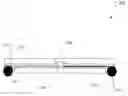
FIG. 1 is an exploded view of the assembly layers of a semiconductor package 100 that uses a thermal conducting substrate 110. In the present embodiment the thermal conducting substrate 110 comprises copper although any substrate material may be used so long as it has an sufficiently high thermal conductivity. In an embodiment the thermal conducting substrate is a laminate of materials with one or any combination of the materials having a sufficiently high thermal conductivity to allow the substrate to operate as a thermally conductive substrate to spread heat from a semiconductor die.
Referring to FIG. 1, the exploded view includes a backing film substrate 115 such as a polyimide tape to bond to the thermal conducting substrate 110. This is just an example, however, any other materials suitable for a backing film substrate may be used. A routing layer such as tape lead 120 is adjacent to the backing film substrate 115 and on the opposite side of the backing film substrate 115 from the thermal conducting substrate 110. In an embodiment the routing layer is copper, yet any conductive material may be used.
The present embodiment has an elastomer layer 125 sandwiched between a tape lead 120 and a semiconductor die 130. The elastomer layer 125 absorbs stress from thermal expansion. The elastomer layer 125 may have openings where the tape lead 120 can connect with the semiconductor die 130. Elastomers are typically polymeric material that may experience large and reversible elastic deformations and are used to absorb stress between layers that may have different coefficients of thermal expansion. Additionally, the present embodiment uses a DRAM die as the semiconductor die 130. Any semiconductor may be used in semiconductor die 130 and be in accordance with the principles of this disclosure. In an embodiment a molded compound 105 may be attached to the conducting substrate 110 as shown in FIG. 1.
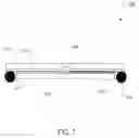
FIG. 2 illustrates a single die assembly 200 consisting of the assembly layers from FIG. 1 resulting in a semiconductor package that uses a thermal conducting substrate 210. In the present embodiment the thermal conducting substrate 210 comprises copper although any substrate material may be used so long as it has a sufficiently high thermal conductivity. In an embodiment the thermal conducting substrate is a laminate of materials with one or any combination of the materials having a sufficiently high thermal conductivity to allow the substrate to operate as a thermally conductive substrate to spread heat from a semiconductor die. A thermal conducting 210 substrate may also connect to ground and act as a ground reference for high-speed signals. In the present embodiment, this ground reference improves signal integrity of the DRAM signals.
Referring to FIG. 2, the assembly 200 includes a backing film substrate 215 such as a polyimide tape that is bonded to the thermal conducting substrate 210. However, any other materials suitable for a backing film substrate may be used. A routing layer such as tape lead 220 is connected to the backing film substrate 215 and on the opposite side of the backing film substrate 215 from the thermal conducting substrate 210. In an embodiment the routing layer is copper, yet any conductive material may be used. The present embodiment also includes solder balls 240 attached to the tape lead 220 at the edge of the assembly 200 and structurally supported by the thermal conducting substrate 210 and the backing film substrate 215. The solder balls 240 may be any other material suitable for electrical interconnection.
The present embodiment has an elastomer layer 225 sandwiched between a tape lead 220 and a semiconductor die 230. The elastomer layer 225 absorbs stress from thermal expansion. In the present embodiment the elastomer layer 225 has openings where the tape lead 220 is connected to the semiconductor die 230. Additionally, the present embodiment uses a DRAM die as the semiconductor die 230. Any semiconductor may be used in semiconductor die 230 and be in accordance with the principles of this disclosure. In an embodiment a mold compound 205 may be attached to the conducting substrate 210 as shown in FIG. 2.
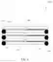
FIG. 3 shows an embodiment multiple die assembly 300 using thermal conducting substrates placed between semiconductor dies such as semiconductor die 130 from FIG. 1. In an embodiment the thermal conducting substrates are each a laminate of materials with one or any combination of the materials having a sufficiently high thermal conductivity to allow the substrate to operate as a thermally conductive substrate to spread heat from a semiconductor die. The multiple die assembly 300 may consist of multiple assemblies 200 from FIG. 2. The embodiment multiple die assembly 300 in FIG. 3 is a stacked configuration including multiple thermally conducting substrates.
In the present embodiment the thermal conducting substrates 310 comprise copper although any substrate material may be used so long as it has an sufficiently high thermal conductivity. A thermal conducting 310 substrate may also connect to ground and act as a ground reference for high-speed signals. Again, this ground reference improves signal integrity to and from any of the semiconductor dies 330.
The multiple die assembly 300 in FIG. 3 includes an elastomer layer 325 in between semiconductor dies and adjacent thermal conductive substrates. Similar to the embodiment illustrated in FIG. 2, a routing layer such as tape lead 320 is connected to the backing film substrate 315 and on the opposite side of the backing film substrate 315 from the thermal conducting substrate 310. The embodiment multiple die assembly 300 also includes connecting balls such as solder balls 340 connecting adjacent assemblies in the multiple die assembly 300. Solder balls 340 are used in the present embodiment but the connecting balls may be any other material suitable for electrical interconnection.
Referring to FIG. 2, the thermally conductive substrate and semiconductor die assembly may be manufactured by the following method. A polymer resin may be adhered to a thermally conductive substrate. In the present embodiment the thermally conductive substrate may be a copper heat spreader, but any suitably heat conductive substrate material may be used. An example polymer resin is a polyimide tape, but embodiments are not limited to use of polyimide tape for the polymer resin.
The method may include attaching a tape lead to the polymer resin. An example tape lead may comprise copper as described in the above apparatus and system, but any material may be used if it can be configured into a routing layer to transport electrical signals. The embodiment method also includes attaching an elastomer to the tape lead. In an embodiment the elastomer has an opening to expose a portion of the tape lead.
The present embodiment includes attaching the elastomer to a die, wherein the die can be any semiconductor die, for example a DRAM die. The method includes attaching the die to the tape lead such as the example embodiment's copper tape lead described above. An embodiment method may further comprise attaching at least one solder ball to the tape lead.
Embodiment methods may include the above method and farther comprise forming a second elastomer layer to the exposed side of the die. Additionally, the present embodiment may further comprise attaching the second elastomer layer to an adjacent heat spreader. In an embodiment these methods may be repeated, thus creating a stacked assembly with multiple heat spreaders.
The present invention may be embodied in other specific forms without departing from its spirit or essential characteristics. The described embodiments are to be considered in all respects only as illustrative instead of restrictive or limiting. Therefore, the scope of the invention is indicated by the appended claims rather than by the foregoing description. All changes, modifications, and alterations that come within the meaning, spirit, and range of equivalency of the claims are to be embraced as being within the scope of the appended claims.
Claims
1. A method comprising:
adhering a polymer resin to a thermally conductive substrate;
attaching a tape lead to the polymer resin;
attaching an elastomer to the tape lead, the elastomer having an opening to expose a portion of the tape lead;
attaching the elastomer to a die; and
attaching the die to the tape lead.
2. The method of claim 1 further comprising, attaching at least one ball to the tape lead.
3. The method of claim 2 wherein the ball is a solder ball.
4. The method of claim 2 further comprising, forming a second elastomer layer to the exposed side of the die.
5. The method of claim 4 further comprising, attaching the second elastomer layer to an adjacent thermally conductive substrate.
6. The method of claim 5 further comprising, repeating the method of claim 14 to create a stacked assembly with thermally conductive substrates.
7. The method of claim 1 wherein the die is a DRAM.
8. The method of claim 1 wherein the polymer resin is a polyimide tape.
9. The method of claim 1 wherein the thermally conductive substrate is a copper heat spreader.
10. The method of claim 1 wherein the tape lead is a copper tape lead.
Images & Drawings included:
Sources:
- United States Patent and Trademark Office - verify current appl. status at the USPTO↗
Similar patent applications:
- » 9923834
Embedded heat spreader ball grid array - » 10389138
Method of fabricating a thin and fine ball-grid array package with embedded heat spreader - » 10389166
Method of fabricating a thin and fine ball-grid array package with embedded heat spreader - » 10388351
Method of fabricating a thin and fine ball-grid array package with embedded heat spreader - » 10389657
Method of fabricating a thin and fine ball-grid array package with embedded heat spreader - » 14286923
Surface mount package for semiconductor devices with embedded heat spreaders - » 20050184370
Embedded heat spreader for folded stacked chip-scale package - » 20060145320
Embedded heat spreader - » 10389352
Method of fabricating a thin and fine ball-grid array package with embedded heat spreader - » 20130168843
Embedded heat spreader for package with multiple microelectronic elements and face-down connection
Recent applications in this class:
- » 20250293106 2025-09-18
SEMICONDUCTOR PACKAGE - » 20250266311 2025-08-21
Methods for Manufacturing Semiconductor Packages - » 20250246492 2025-07-31
IC PACKAGE WITH INTERCONNECT - » 20250218882 2025-07-03
CHIP INTEGRATION INTO CAVITIES OF A HOST WAFER USING LATERAL DIELECTRIC MATERIAL BONDING - » 20250191988 2025-06-12
HEAT DISSIPATION THROUGH SEAL RINGS - » 20250105077 2025-03-27
PACKAGE-ON-PACKAGE STRUCTURE AND MANUFACTURING METHOD THEREOF - » 20250105076 2025-03-27
SEMICONDUCTOR PACKAGE FOR A PCB - » 20250069975 2025-02-27
SEMICONDUCTOR STRUCTURE HAVING AN ANTI-ARCING PATTERN DISPOSED ON A PASSIVATION LAYER - » 20250069974 2025-02-27
WAFER LEVEL PACKAGING COMPONENT HAVING SIDE WETTABLE STRUCTURE - » 20250069973 2025-02-27
CHIP SCALE SEMICONDUCTOR PACKAGE HAVING BACK SIDE METAL LAYER AND RAISED FRONT SIDE PAD AND METHOD OF MAKING THE SAME
Recent applications for this Assignee:
- » 20250294866 2025-09-18
GATE CUT CONFINED WITHIN GATE TRENCH - » 20250294846 2025-09-18
BACKSIDE CROSS-COUPLE INTERCONNECTS - » 20250294835 2025-09-18
ELONGATED VERTICAL STRUCTURES OF CHANNEL MATERIALS - » 20250294827 2025-09-18
CO-INTEGRATION OF GATE-ALL-AROUND DEVICES WITH DIFFERENT NUMBERS OF NANORIBBONS - » 20250294818 2025-09-18
TRANSISTOR DESIGNS FOR FLOATING BODY MEMORY - » 20250294781 2025-09-18
MAGNETIC CORE INDUCTORS ON PACKAGE SUBSTRATES - » 20250294777 2025-09-18
INTEGRATED CIRCUIT DEVICE WITH MEMORY ARRAY AND SHARED GAIN ELEMENT - » 20250293985 2025-09-18
RECEIVER-BASED PRECISION CONGESTION CONTROL - » 20250293860 2025-09-18
PRESERVATION OF CONFIDENTIALITY AND INTEGRITY OF MODELS DURING EXECUTION - » 20250293706 2025-09-18
LOW-RANK DECOMPOSITION-BASED HARDWARE COMPRESSION OF MATRICES AND TENSORS