Gold/silicon eutectic die bonding method
US20080124838A1
2008-05-29
11/605,831
2006-11-27
✅ Patent granted
US 7,659,191 B2
2010-02-09
-
-
Alexander G Ghyka | Seahvosh J Nikmanesh
2027-06-30
Abstract:
A direct gold/silicon eutectic die bonding method is disclosed. The method includes the steps of gold plating a die bonding pad, grinding a wafer to a desired thickness, dicing the wafer after the grinding step, picking a die, and attaching the die to the die bonding pad at a temperature above the gold/silicon eutectic temperature. For thinner wafers, a dicing before grinding process is employed.
Assignee:
- Alpha and Omega Semiconductor Incorporated 478 🇺🇸 Sunnyvale, CA, United States
Interested in similar patents?
Get notified when new applications in this technology area are published.
Classification:
H01L21/46 IPC
Processes or apparatus adapted for the manufacture or treatment of semiconductor or solid state devices or of parts thereof; Manufacture or treatment of semiconductor devices or of parts thereof the devices having at least one potential-jump barrier or surface barrier, e.g. PN junction, depletion layer or carrier concentration layer the devices having semiconductor bodies not provided for in groups, , , and with or without impurities, e.g. doping materials Treatment of semiconductor bodies using processes or apparatus not provided for in groups
H01L24/33 » CPC main
Arrangements for connecting or disconnecting semiconductor or solid-state bodies; Methods or apparatus related thereto; Means for bonding being attached to, or being formed on, the surface to be connected, e.g. chip-to-package, die-attach, "first-level" interconnects; Manufacturing methods related thereto; Layer connectors, e.g. plate connectors, solder or adhesive layers; Manufacturing methods related thereto; Structure, shape, material or disposition of the layer connectors after the connecting process of a plurality of layer connectors
H01L24/83 » CPC further
Arrangements for connecting or disconnecting semiconductor or solid-state bodies; Methods or apparatus related thereto; Methods for connecting semiconductor or other solid state bodies using means for bonding being attached to, or being formed on, the surface to be connected using a layer connector
H01L23/49582 » CPC further
Details of semiconductor or other solid state devices; Arrangements for conducting electric current to or from the solid state body in operation, e.g. leads, terminal arrangements ; Selection of materials therefor consisting of soldered constructions; Lead-frames or other flat leads characterised by the materials of the lead frames or layers thereon Metallic layers on lead frames
H01L2224/83801 » CPC further
Indexing scheme for arrangements for connecting or disconnecting semiconductor or solid-state bodies and methods related thereto as covered by; Methods for connecting semiconductor or other solid state bodies using means for bonding being attached to, or being formed on, the surface to be connected using a layer connector; Bonding techniques Soldering or alloying
H01L2224/83894 » CPC further
Indexing scheme for arrangements for connecting or disconnecting semiconductor or solid-state bodies and methods related thereto as covered by; Methods for connecting semiconductor or other solid state bodies using means for bonding being attached to, or being formed on, the surface to be connected using a layer connector; Bonding techniques Direct bonding, i.e. joining surfaces by means of intermolecular attracting interactions at their interfaces, e.g. covalent bonds, van der Waals forces
H01L2924/01006 » CPC further
Indexing scheme for arrangements or methods for connecting or disconnecting semiconductor or solid-state bodies as covered by; Chemical elements Carbon [C]
H01L2924/01023 » CPC further
Indexing scheme for arrangements or methods for connecting or disconnecting semiconductor or solid-state bodies as covered by; Chemical elements Vanadium [V]
H01L2924/01033 » CPC further
Indexing scheme for arrangements or methods for connecting or disconnecting semiconductor or solid-state bodies as covered by; Chemical elements Arsenic [As]
H01L2924/01078 » CPC further
Indexing scheme for arrangements or methods for connecting or disconnecting semiconductor or solid-state bodies as covered by; Chemical elements Platinum [Pt]
H01L2924/01079 » CPC further
Indexing scheme for arrangements or methods for connecting or disconnecting semiconductor or solid-state bodies as covered by; Chemical elements Gold [Au]
H01L2924/01082 » CPC further
Indexing scheme for arrangements or methods for connecting or disconnecting semiconductor or solid-state bodies as covered by; Chemical elements Lead [Pb]
H01L2924/01322 » CPC further
Indexing scheme for arrangements or methods for connecting or disconnecting semiconductor or solid-state bodies as covered by; Alloys; Binary Alloys Eutectic Alloys, i.e. obtained by a liquid transforming into two solid phases
H01L2924/014 » CPC further
Indexing scheme for arrangements or methods for connecting or disconnecting semiconductor or solid-state bodies as covered by; Alloys Solder alloys
H01L2924/10253 » CPC further
Indexing scheme for arrangements or methods for connecting or disconnecting semiconductor or solid-state bodies as covered by; Details of semiconductor or other solid state devices to be connected; Material of the semiconductor or solid state bodies; Semiconducting materials; Elemental semiconductors, i.e. Group IV Silicon [Si]
H01L2924/13091 » CPC further
Indexing scheme for arrangements or methods for connecting or disconnecting semiconductor or solid-state bodies as covered by; Details of semiconductor or other solid state devices to be connected; Device type; Discrete devices, e.g. 3 terminal devices; Transistor; Field-effect transistor [FET] Metal-Oxide-Semiconductor Field-Effect Transistor [MOSFET]
H01L2924/01014 » CPC further
Indexing scheme for arrangements or methods for connecting or disconnecting semiconductor or solid-state bodies as covered by; Chemical elements Silicon [Si]
H01L2924/0665 » CPC further
Indexing scheme for arrangements or methods for connecting or disconnecting semiconductor or solid-state bodies as covered by; Polymers Epoxy resin
H01L2924/00 » CPC further
Indexing scheme for arrangements or methods for connecting or disconnecting semiconductor or solid-state bodies as covered by
H01L21/60 IPC
Processes or apparatus adapted for the manufacture or treatment of semiconductor or solid state devices or of parts thereof; Manufacture or treatment of semiconductor devices or of parts thereof the devices having at least one potential-jump barrier or surface barrier, e.g. PN junction, depletion layer or carrier concentration layer; Assembly of semiconductor devices using processes or apparatus not provided for in a single one of the subgroups - , e.g. sealing of a cap to a base of a container Attaching or detaching leads or other conductive members, to be used for carrying current to or from the device in operation
H01L21/00 IPC
Processes or apparatus adapted for the manufacture or treatment of semiconductor or solid state devices or of parts thereof
H01L21/76 IPC
Processes or apparatus adapted for the manufacture or treatment of semiconductor or solid state devices or of parts thereof; Manufacture or treatment of devices consisting of a plurality of solid state components formed in or on a common substrate or of parts thereof; Manufacture of integrated circuit devices or of parts thereof; Manufacture of specific parts of devices defined in group Making of isolation regions between components
H01L21/30 IPC
Processes or apparatus adapted for the manufacture or treatment of semiconductor or solid state devices or of parts thereof; Manufacture or treatment of semiconductor devices or of parts thereof the devices having at least one potential-jump barrier or surface barrier, e.g. PN junction, depletion layer or carrier concentration layer the devices having semiconductor bodies comprising elements of Group IV of the Periodic System or AB compounds with or without impurities, e.g. doping materials Treatment of semiconductor bodies using processes or apparatus not provided for in groups -
H01L21/44 IPC
Processes or apparatus adapted for the manufacture or treatment of semiconductor or solid state devices or of parts thereof; Manufacture or treatment of semiconductor devices or of parts thereof the devices having at least one potential-jump barrier or surface barrier, e.g. PN junction, depletion layer or carrier concentration layer the devices having semiconductor bodies not provided for in groups, , , and with or without impurities, e.g. doping materials Manufacture of electrodes on semiconductor bodies using processes or apparatus not provided for in groups -
Description
BACKGROUND OF THE INVENTION
The present invention generally relates to a method of bonding a semiconductor die to a package and more particularly to a direct gold/silicon eutectic bonding method.
Conventional die bonding methods include a wide choice of materials that are used in the attachment of silicon dies (with or without back metal) to substrates. These materials include hard and soft solders, conductive epoxies, and gold/silicon eutectic alloys. Gold/silicon eutectic alloys are the preferred choice for small packages such as SOT-23 and SOT-363 and are the only choice for even smaller packages such as SOT-563 and SOT-623.
Conventional gold/silicon eutectic die bonding methods include coating the back surface of the silicon die with gold and then heating the die to a temperature above the eutectic temperature of 370° C. to form the gold/silicon eutectic alloy. In most applications, an adhesion layer of sandwich type structure is used to improve the adhesion of the gold to the silicon die. The die is then attached to a metal leadframe or substrate by an additional heating step which utilizes the gold/silicon eutectic alloy as a solder. Additional layers of gold may be deposited over the gold/silicon eutectic alloy layer and gold or gold alloy pre-forms may be used to facilitate die bonding. Other conventional techniques include using a gold/silicon seed as a catalyst for forming the eutectic bond and using a gold/silicon alloy produced by silicon implantation in a gold layer.
Increased performance requirements of vertical power device products are driving manufacturers to integrate and assemble these devices using thinner wafer processes. Prior art methods of coating the back surface of silicon die formed on thin wafers with metal present difficulties. There is therefore a need for a die bonding method that is simple and does not require a back metal process. There is also a need for a die bonding method that does not require a pre-form, eutectic solder, or seed implant. There is a further need for a die bonding method that is cost efficient and that increases device throughput.
SUMMARY OF THE INVENTION
The problems associated with the bonding of vertical power devices formed on thin wafers to package substrates are solved by the direct gold/silicon eutectic die bonding method of the invention. In accordance with a method of the invention, a die pad of a leadframe is first plated with gold. Then a wafer is either ground to a desired thickness and diced, or alternatively, diced before being ground to the desired thickness using a dice before grinding process . The device is then picked from a dicing tape and attached to the gold plated leadframe die pad at a pre-defined temperature higher than the gold/silicon eutectic temperature of 370° C. to thereby form a gold/silicon eutectic alloy. The silicon on the back side of the die and the gold on the surface of the leadframe can penetrate the silicon oxide layer to form the gold/silicon eutectic alloy with the help of supersonic power and the increase temperature.
In accordance with one aspect of the invention, a gold/silicon eutectic die bonding method includes the steps of gold plating a die bonding pad, grinding a wafer to a desired thickness, dicing the wafer after the grinding step, picking a die, and attaching the die to the die bonding pad at a temperature above the gold/silicon eutectic temperature.
In accordance with another aspect of the invention, a gold/silicon eutectic die bonding method includes the steps of gold plating a die bonding pad, dicing the wafer, grinding the wafer to a desired thickness after the dicing step, picking a die, and attaching the die to the die bonding pad at a temperature above the gold/silicon eutectic temperature.
There has been outlined, rather broadly, the more important features of the invention in order that the detailed description thereof that follows may be better understood, and in order that the present contribution to the art may be better appreciated. There are, of course, additional features of the invention that will be described below and which will form the subject matter of the claims appended herein.
In this respect, before explaining at least one embodiment of the invention in detail, it is to be understood that the invention is not limited in its application to the details of the method set forth in the following description or illustrated in the drawings. The invention is capable of other embodiments and of being practiced and carried out in various ways. Also, it is to be understood that the phraseology and terminology employed herein, as well as the abstract, are for the purpose of description and should not be regarded as limiting.
As such, those skilled in the art will appreciate that the conception upon which this disclosure is based may readily be utilized as a basis for the designing of other structures, methods and systems for carrying out the several purposes of the present invention. It is important, therefore, that the claims be regarded as including such equivalent constructions insofar as they do not depart from the spirit and scope of the present invention.
These and other features, aspects and advantages of the present invention will become better understood with reference to the following drawings, description and claims.
BRIEF DESCRIPTION OF THE DRAWINGS
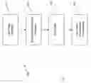
FIG. 1 is a flow chart showing a gold/silicon eutectic die bonding method in accordance with the invention;
FIG. 2 is a flow chart showing an alternate gold/silicon eutectic die bonding method in accordance with the invention; and
FIG. 3 is a cross sectional view of die bonded to a leadframe showing the gold/silicon eutectic layer in accordance with the invention.
DETAILED DESCRIPTION OF THE INVENTION
The present invention provides a gold/silicon eutectic die bonding method for directly attaching a die to a gold plated leadframe without the need for a wafer back metal process.
With reference to FIG. 1, the method 100 of the invention includes a step 110 in which a die pad of a leadframe is gold plated. In a step 120, the backside of a vertical power MOSFET silicon wafer is ground to a desired thickness, for example, 8 mil. The wafer is then diced in a step 130. The die are then picked from a dicing tape and attached to the die pad in a step 140 at a pre-defined temperature higher than the gold/silicon eutectic temperature of 370° C. to thereby form a gold/silicon eutectic alloy. The silicon on the back side of the die and the gold on the surface of the leadframe die pad can penetrate the silicon oxide layer by scribing or supersonic power at a high enough temperature to form the eutectic alloy.
Experimental results show that for a die size of 0.5 mm by 0.5 mm, a temperature of 420° C. is sufficient to achieve a gold/silicon eutectic bond. For die sizes of 1.0 mm by 1.0 mm and 2.0 mm by 2.0 mm, a temperature of 440° C. was sufficient. A cross sectional view of a gold/silicon eutectic bond 300 formed between a die 305 and a leadframe 310 is represented in FIG. 3.
An alternative method 200 of the invention includes a step 210 in which a die pad of a leadframe is gold plated. In a step 220, the vertical power MOSFET wafer is diced from a top surface 307 to a predetermined depth that is deeper than the desired thickness of finished die but shallower than the wafer thickness so that the die are not separate. In a step 230 a back surface 309 of the wafer are ground to a desired thickness such as by a dicing before grinding process. The wafer may be ground to a thickness of between 3 and 4 mil or any desired thickness that is less then the dicing depth to thereby separate the die. Alternatively the wafer may be diced through and the die are separated before grinding. Finally, in a step 240 the die are picked from a dicing tape and attached to the die pad at a pre-defined temperature higher than the gold/silicon eutectic temperature of 370° C. to form a gold/silicon eutectic alloy. The silicon on the back side of the die and the gold on the surface of the leadframe die pad can penetrate the silicon oxide layer by scribing or supersonic power at a high enough temperature to form the eutectic alloy.
The direct gold/silicon eutectic die bonding methods in accordance with the invention provide gold/silicon eutectic die bonding methods that do not require a wafer back metal process. As such the die bonding methods are cost efficient and provide for increased device throughput.
It should be understood, of course, that the foregoing relates to preferred embodiments of the invention and that modifications may be made without departing from the spirit and scope of the invention as set forth in the following claims.
Claims
We claim:1. A gold/silicon eutectic die bonding method comprising the steps of:
gold plating a die bonding pad;
grinding a wafer to a desired thickness;
dicing the wafer after the grinding step;
picking a die; and
attaching the die to the die bonding pad at a temperature above the gold/silicon eutectic temperature.
2. The gold/silicon eutectic die bonding method of claim 1, wherein the die comprises a vertical power device.
3. The gold/silicon eutectic die bonding method of claim 1, wherein the die are 0.5 mm by 0.5 mm and the temperature is 420° C.
4. The gold/silicon eutectic die bonding method of claim 1, wherein the die are 1.0 mm by 1.0 mm and the temperature is 440° C.
5. The gold/silicon eutectic die bonding method of claim 1, wherein the die are 2.0 mm by 2.0 mm and the temperature is 440° C.
6. A gold/silicon eutectic die bonding method comprising the steps of:
gold plating a die bonding pad;
dicing the wafer from a top surface to a predetermined depth;. grinding the wafer back surface to a desired thickness after the dicing step;
picking a die; and
attaching the die to the die bonding pad at a temperature above the gold/silicon eutectic temperature.
7. The gold/silicon eutectic die bonding method of claim 6, wherein the die comprises a vertical power device.
8. The gold/silicon eutectic die bonding method of claim 6, wherein the wafer is diced to a depth shallower than a thickness of the wafer.
9. The gold/silicon eutectic die bonding method of claim 6, wherein the die are ground to a thickness of between 3 and 4 mils.
10. The gold/silicon eutectic die bonding method of claim 6, wherein the die are 0.5 mm by 0.5 mm and the temperature is 420° C.
11. The gold/silicon eutectic die bonding method of claim 6, wherein the die are 1.0 mm by 1.0 mm and the temperature is 440° C.
12. The gold/silicon eutectic die bonding method of claim 6, wherein the die are 2.0 mm by 2.0 mm and the temperature is 440° C.
Images & Drawings included:


Sources:
- United States Patent and Trademark Office - verify current appl. status at the USPTO↗
Similar patent applications:
- » 20070231954
Gold/silicon eutectic die bonding method
Recent applications in this class:
- » 20250233098 2025-07-17
SEMICONDUCTOR DEVICE - » 20250054900 2025-02-13
SEMICONDUCTOR PACKAGE AND MANUFACTURING METHOD THEREOF - » 20240321810 2024-09-26
CHIP PACKAGE STRUCTURE - » 20240312945 2024-09-19
ELECTRONIC DEVICE AND DISPLAY DEVICE USING THE SAME - » 20240250055 2024-07-25
PACKAGE STRUCTURE WITH PROTECTIVE LID - » 20240170440 2024-05-23
SEMICONDUCTOR PACKAGE - » 20240162184 2024-05-16
SEMICONDUCTOR PACKAGE - » 20240079366 2024-03-07
SEMICONDUCTOR PACKAGE - » 20240071977 2024-02-29
DIE EDGE FILLET AND 3D-PRINTED CNT AS BENDING STRESS BUFFER - » 20230402420 2023-12-14
SEMICONDUCTOR DEVICE AND METHOD FOR MANUFACTURING THE SAME
Recent applications for this Assignee:
- » 20210210954 2021-07-08
USB type-C load switch ESD protection - » 20210020567 2021-01-21
Dual-gate trench IGBT with buried floating P-type shield - » 20200381513 2020-12-03
Semiconductor chip integrating high and low voltage devices - » 20200303513 2020-09-24
Sawtooh electric field drift region structure for planar and trench power semiconductor devices - » 20190393218 2019-12-26
Bidirectional switch having back to back field effect transistors - » 20190355844 2019-11-21
Asymmetrical blocking bidirectional gallium nitride switch - » 20190296157 2019-09-26
Vertical gallium nitride Schottky diode - » 20190214261 2019-07-11
Semiconductor device and method of forming including superjunction structure formed using angled implant process - » 20190172945 2019-06-06
Method for fabricating a folded channel trench MOSFET - » 20190165169 2019-05-30
Method for forming a lateral super-junction MOSFET device and termination structure