Integrated circuit package system with leads having multiple sides exposed
US20080171405A1
2008-07-17
12/014,578
2008-01-15
✅ Patent granted
US 8,847,413 B2
2014-09-30
-
-
Julio J Maldonado | Mohammad Choudhry
Ishimaru & Associates LLP
2031-03-12
Abstract:
An integrated circuit package system includes forming an integrated circuit stack having a bottom non-active side and a top non-active side; connecting an internal interconnect between a lead, having a top side and a bottom side, and the integrated circuit stack; and forming an encapsulation, having both a non-elevated portion and an elevated portion, around the integrated circuit stack and the internal interconnect with the top side exposed at the non-elevated portion, and with the bottom side, the bottom non-active side, and the top non-active side exposed.
Assignee:
- STATS CHIPPAC, LTD. 1,631 🇸🇬 Singapore, Singapore
Applicant:
Interested in similar patents?
Get notified when new applications in this technology area are published.
Classification:
H01L21/568 » CPC further
Processes or apparatus adapted for the manufacture or treatment of semiconductor or solid state devices or of parts thereof; Manufacture or treatment of semiconductor devices or of parts thereof the devices having at least one potential-jump barrier or surface barrier, e.g. PN junction, depletion layer or carrier concentration layer; Assembly of semiconductor devices using processes or apparatus not provided for in a single one of the subgroups - , e.g. sealing of a cap to a base of a container; Encapsulations, e.g. encapsulation layers, coatings Temporary substrate used as encapsulation process aid
H01L2225/0651 » CPC further
Details relating to assemblies covered by the group but not provided for in its subgroups; All the devices being of a type provided for in the same subgroup of groups - the devices not having separate containers the devices being of a type provided for in group; Stacked arrangements of devices Wire or wire-like electrical connections from device to substrate
H01L25/03 » CPC further
Assemblies consisting of a plurality of individual semiconductor or other solid state devices ; Multistep manufacturing processes thereof all the devices being of a type provided for in the same subgroup of groups - , e.g. assemblies of rectifier diodes
H01L2224/73265 » CPC further
Indexing scheme for arrangements for connecting or disconnecting semiconductor or solid-state bodies and methods related thereto as covered by; Means for bonding being of different types provided for in two or more of groups; Location after the connecting process on different surfaces Layer and wire connectors
H01L2924/00014 » CPC further
Indexing scheme for arrangements or methods for connecting or disconnecting semiconductor or solid-state bodies as covered by; Technical content checked by a classifier the subject-matter covered by the group, the symbol of which is combined with the symbol of this group, being disclosed without further technical details
H01L2224/85 » CPC further
Indexing scheme for arrangements for connecting or disconnecting semiconductor or solid-state bodies and methods related thereto as covered by; Methods for connecting semiconductor or other solid state bodies using means for bonding being attached to, or being formed on, the surface to be connected using a wire connector
H01L2224/83 » CPC further
Indexing scheme for arrangements for connecting or disconnecting semiconductor or solid-state bodies and methods related thereto as covered by; Methods for connecting semiconductor or other solid state bodies using means for bonding being attached to, or being formed on, the surface to be connected using a layer connector
H01L2924/181 » CPC further
Indexing scheme for arrangements or methods for connecting or disconnecting semiconductor or solid-state bodies as covered by; Details of package parts other than the semiconductor or other solid state devices to be connected Encapsulation
H01L2924/00012 » CPC further
Indexing scheme for arrangements or methods for connecting or disconnecting semiconductor or solid-state bodies as covered by; Technical content checked by a classifier Relevant to the scope of the group, the symbol of which is combined with the symbol of this group
H01L2924/00 » CPC further
Indexing scheme for arrangements or methods for connecting or disconnecting semiconductor or solid-state bodies as covered by
H01L21/60 IPC
Processes or apparatus adapted for the manufacture or treatment of semiconductor or solid state devices or of parts thereof; Manufacture or treatment of semiconductor devices or of parts thereof the devices having at least one potential-jump barrier or surface barrier, e.g. PN junction, depletion layer or carrier concentration layer; Assembly of semiconductor devices using processes or apparatus not provided for in a single one of the subgroups - , e.g. sealing of a cap to a base of a container Attaching or detaching leads or other conductive members, to be used for carrying current to or from the device in operation
H01L23/49575 » CPC main
Details of semiconductor or other solid state devices; Arrangements for conducting electric current to or from the solid state body in operation, e.g. leads, terminal arrangements ; Selection of materials therefor consisting of soldered constructions; Lead-frames or other flat leads Assemblies of semiconductor devices on lead frames
H01L31/0203 » CPC further
Semiconductor devices sensitive to infra-red radiation, light, electromagnetic radiation of shorter wavelength or corpuscular radiation and specially adapted either for the conversion of the energy of such radiation into electrical energy or for the control of electrical energy by such radiation; Processes or apparatus specially adapted for the manufacture or treatment thereof or of parts thereof; Details thereof; Details Containers; Encapsulations, e.g. encapsulation of photodiodes
H01L23/3107 » CPC further
Details of semiconductor or other solid state devices; Encapsulations, e.g. encapsulating layers, coatings, e.g. for protection characterised by the arrangement or shape the device being completely enclosed
H01L23/3128 » CPC further
Details of semiconductor or other solid state devices; Encapsulations, e.g. encapsulating layers, coatings, e.g. for protection characterised by the arrangement or shape the device being completely enclosed a substrate forming part of the encapsulation the substrate having spherical bumps for external connection
H01L23/3135 » CPC further
Details of semiconductor or other solid state devices; Encapsulations, e.g. encapsulating layers, coatings, e.g. for protection characterised by the arrangement or shape the device being completely enclosed Double encapsulation or coating and encapsulation
H01L23/49548 » CPC further
Details of semiconductor or other solid state devices; Arrangements for conducting electric current to or from the solid state body in operation, e.g. leads, terminal arrangements ; Selection of materials therefor consisting of soldered constructions; Lead-frames or other flat leads; Geometry of the lead-frame Cross section geometry
H01L24/45 » CPC further
Arrangements for connecting or disconnecting semiconductor or solid-state bodies; Methods or apparatus related thereto; Means for bonding being attached to, or being formed on, the surface to be connected, e.g. chip-to-package, die-attach, "first-level" interconnects; Manufacturing methods related thereto; Wire connectors; Manufacturing methods related thereto; Structure, shape, material or disposition of the wire connectors prior to the connecting process of an individual wire connector
H01L24/97 » CPC further
Arrangements for connecting or disconnecting semiconductor or solid-state bodies; Methods or apparatus related thereto; Batch processes at chip-level, i.e. with connecting carried out on a plurality of singulated devices, i.e. on diced chips the devices being connected to a common substrate, e.g. interposer, said common substrate being separable into individual assemblies after connecting
H01L25/0657 » CPC further
Assemblies consisting of a plurality of individual semiconductor or other solid state devices ; Multistep manufacturing processes thereof all the devices being of a type provided for in the same subgroup of groups - , e.g. assemblies of rectifier diodes the devices not having separate containers the devices being of a type provided for in group Stacked arrangements of devices
H01L25/105 » CPC further
Assemblies consisting of a plurality of individual semiconductor or other solid state devices ; Multistep manufacturing processes thereof all the devices being of a type provided for in the same subgroup of groups - , e.g. assemblies of rectifier diodes the devices having separate containers the devices being of a type provided for in group
H01L2224/97 » CPC further
Indexing scheme for arrangements for connecting or disconnecting semiconductor or solid-state bodies and methods related thereto as covered by; Batch processes at chip-level, i.e. with connecting carried out on a plurality of singulated devices, i.e. on diced chips the devices being connected to a common substrate, e.g. interposer, said common substrate being separable into individual assemblies after connecting
H01L2225/06562 » CPC further
Details relating to assemblies covered by the group but not provided for in its subgroups; All the devices being of a type provided for in the same subgroup of groups - the devices not having separate containers the devices being of a type provided for in group; Stacked arrangements of devices; Geometry of the stack, e.g. form of the devices, geometry to facilitate stacking at least one device in the stack being rotated or offset
H01L2924/01013 » CPC further
Indexing scheme for arrangements or methods for connecting or disconnecting semiconductor or solid-state bodies as covered by; Chemical elements Aluminum [Al]
H01L2924/01029 » CPC further
Indexing scheme for arrangements or methods for connecting or disconnecting semiconductor or solid-state bodies as covered by; Chemical elements Copper [Cu]
H01L2924/01046 » CPC further
Indexing scheme for arrangements or methods for connecting or disconnecting semiconductor or solid-state bodies as covered by; Chemical elements Palladium [Pd]
H01L2924/01079 » CPC further
Indexing scheme for arrangements or methods for connecting or disconnecting semiconductor or solid-state bodies as covered by; Chemical elements Gold [Au]
H01L2924/01082 » CPC further
Indexing scheme for arrangements or methods for connecting or disconnecting semiconductor or solid-state bodies as covered by; Chemical elements Lead [Pb]
H01L2924/14 » CPC further
Indexing scheme for arrangements or methods for connecting or disconnecting semiconductor or solid-state bodies as covered by; Details of semiconductor or other solid state devices to be connected; Device type Integrated circuits
H01L2924/15311 » CPC further
Indexing scheme for arrangements or methods for connecting or disconnecting semiconductor or solid-state bodies as covered by; Details of package parts other than the semiconductor or other solid state devices to be connected; Die mounting substrate; Connection portion the connection portion being formed only on the surface of the substrate opposite to the die mounting surface being a ball array, e.g. BGA
H01L24/48 » CPC further
Arrangements for connecting or disconnecting semiconductor or solid-state bodies; Methods or apparatus related thereto; Means for bonding being attached to, or being formed on, the surface to be connected, e.g. chip-to-package, die-attach, "first-level" interconnects; Manufacturing methods related thereto; Wire connectors; Manufacturing methods related thereto; Structure, shape, material or disposition of the wire connectors after the connecting process of an individual wire connector
H01L2924/01033 » CPC further
Indexing scheme for arrangements or methods for connecting or disconnecting semiconductor or solid-state bodies as covered by; Chemical elements Arsenic [As]
H01L2924/01028 » CPC further
Indexing scheme for arrangements or methods for connecting or disconnecting semiconductor or solid-state bodies as covered by; Chemical elements Nickel [Ni]
H01L2225/1029 » CPC further
Details relating to assemblies covered by the group but not provided for in its subgroups; All the devices being of a type provided for in the same subgroup of groups - the devices having separate containers the devices being of a type provided for in group the containers being in a stacked arrangement the lowermost container comprising a device support the support being a lead frame
H01L2225/1052 » CPC further
Details relating to assemblies covered by the group but not provided for in its subgroups; All the devices being of a type provided for in the same subgroup of groups - the devices having separate containers the devices being of a type provided for in group the containers being in a stacked arrangement; Details of electrical connections between containers Wire or wire-like electrical connections
H01L2924/3511 » CPC further
Indexing scheme for arrangements or methods for connecting or disconnecting semiconductor or solid-state bodies as covered by; Technical effects; Mechanical effects; Thermal stress Warping
H01L2924/12041 » CPC further
Indexing scheme for arrangements or methods for connecting or disconnecting semiconductor or solid-state bodies as covered by; Details of semiconductor or other solid state devices to be connected; Device type; Passive devices, e.g. 2 terminal devices; Optical Diode LED
H01L23/495 IPC
Details of semiconductor or other solid state devices; Arrangements for conducting electric current to or from the solid state body in operation, e.g. leads, terminal arrangements ; Selection of materials therefor consisting of soldered constructions Lead-frames or other flat leads
H01L21/56 IPC
Processes or apparatus adapted for the manufacture or treatment of semiconductor or solid state devices or of parts thereof; Manufacture or treatment of semiconductor devices or of parts thereof the devices having at least one potential-jump barrier or surface barrier, e.g. PN junction, depletion layer or carrier concentration layer; Assembly of semiconductor devices using processes or apparatus not provided for in a single one of the subgroups - , e.g. sealing of a cap to a base of a container Encapsulations, e.g. encapsulation layers, coatings
H01L23/31 IPC
Details of semiconductor or other solid state devices; Encapsulations, e.g. encapsulating layers, coatings, e.g. for protection characterised by the arrangement or shape
H01L25/065 IPC
Assemblies consisting of a plurality of individual semiconductor or other solid state devices ; Multistep manufacturing processes thereof all the devices being of a type provided for in the same subgroup of groups - , e.g. assemblies of rectifier diodes the devices not having separate containers the devices being of a type provided for in group
H01L25/10 IPC
Assemblies consisting of a plurality of individual semiconductor or other solid state devices ; Multistep manufacturing processes thereof all the devices being of a type provided for in the same subgroup of groups - , e.g. assemblies of rectifier diodes the devices having separate containers
H01L23/00 IPC
Details of semiconductor or other solid state devices
Description
CROSS-REFERENCE TO RELATED APPLICATION
This application claims the benefit of U.S. Provisional Patent Application Ser. No. 60/884,999 filed Jan. 15, 2007.
TECHNICAL FIELD
The present invention relates generally to integrated circuit package systems, and more particularly to a system for integrated circuit package systems having stacked packages.
BACKGROUND ART
To interface an integrated circuit with other circuitry, it is common to mount it on a lead frame or substrate. Each integrated circuit has bonding pads that are individually connected to the lead frame's lead finger pads using extremely fine gold or aluminum wires. The assemblies are then packaged by individually encapsulating them in molded plastic or ceramic bodies to create an integrated circuit package.
Integrated circuit packaging technology has seen an increase in the number of integrated circuits mounted on a single circuit board or substrate. The new packaging designs are more compact in form factors, such as the physical size and shape of an integrated circuit, and providing a significant increase in overall integrated circuit density.
However, integrated circuit density continues to be limited by the “real estate” available for mounting individual integrated circuits on a substrate. Even larger form factor systems, such as PC's, compute servers, and storage servers, need more integrated circuits in the same or smaller “real estate”. Particularly acute, the needs for portable personal electronics, such as cell phones, digital cameras, music players, PDA's, and location-based devices, have further driven the need for integrated circuit density.
This need for increased integrated circuit density, has led to the development of multi-chip packages in which more than one integrated circuit can be packaged. Each package provides mechanical support for the individual integrated circuits and one or more layers of interconnect lines that enable the integrated circuits to be connected electrically to surrounding circuitry.
Current multi-chip packages, also commonly referred to as multi-chip modules, typically consist of one or more substrates onto each of which one or more integrated circuit components is directly attached. Such multi-chip packages have been found to increase integrated circuit density and miniaturization, improve signal propagation speed, reduce overall integrated circuit size and weight, improve performance, and lower costs—all primary goals of the computer industry.
There is always a limitation on the number of die that can be stacked in a package, especially for big memory dice. Same die stacking with all bond pads at one side allows stacking in the staircase manner that eliminates the need for thick spacers between the dice. However, stacking is still restricted by the package size where over-stacking cause die protrusion requiring extra long packages.
Thus, a need still remains for improved packaging methods, systems, and designs. In view of the shrinking size of consumer electronics and the demand for more sophisticated functions in the restricted space, it is increasingly critical that answers be found to these problems. In view of the ever-increasing commercial competitive pressures, increasing consumer expectations, and diminishing opportunities for meaningful product differentiation in the marketplace, it is increasingly critical that answers be found to these problems. Moreover, the ever-increasing need to save costs, improve efficiencies, and meet such competitive pressures adds even greater urgency to the critical necessity that answers be found to these problems.
Solutions to these problems have been long sought but prior developments have not taught or suggested any solutions and, thus, solutions to these problems have long eluded those skilled in the art.
DISCLOSURE OF THE INVENTION
The present invention provides an integrated circuit package system that includes forming an integrated circuit stack having a bottom non-active side and a top non-active side; connecting an internal interconnect between a lead, having a top side and a bottom side, and the integrated circuit stack; and forming an encapsulation, having both an non-elevated portion and an elevated portion, around the integrated circuit stack and the internal interconnect with the top side exposed at the non-elevated portion, and with the bottom side, the bottom non-active side, and the top non-active side exposed.
Certain embodiments of the invention have other aspects in addition to or in place of those mentioned above. The aspects will become apparent to those skilled in the art from a reading of the following detailed description when taken with reference to the accompanying drawings.
BRIEF DESCRIPTION OF THE DRAWINGS
FIG. 1 is a top view of an integrated circuit package system in a first embodiment of the present invention;
FIG. 2 is a bottom view of the integrated circuit package system of FIG. 1;
FIG. 3 is a cross-sectional view of the integrated circuit package system along 3-3 of FIG. 1;
FIG. 4 is a top view of an integrated circuit package system in a second embodiment of the present invention;
FIG. 5 is a bottom view of the integrated circuit package system of FIG. 4;
FIG. 6 is a cross-sectional view of the integrated circuit package system along 6-6 of FIG. 4;
FIG. 7 is a cross-sectional view of an integrated circuit package system in a third embodiment of the present invention;
FIG. 8 is a cross-sectional view of an integrated circuit package system in a fourth embodiment of the present invention;
FIG. 9 is a cross-sectional view of a portion of a lead frame in a die attaching step of a portion the integrated circuit stack of FIG. 3;
FIG. 10 is the structure of FIG. 9 in a connecting step of the internal interconnects;
FIG. 11 is the structure of FIG. 10 in a forming step of the encapsulation;
FIG. 12 is the structure of FIG. 11 in a singulating step of the integrated circuit package system of FIG. 3; and
FIG. 13 is a flow chart of an integrated circuit package system for manufacturing of the integrated circuit package system in an embodiment of the present invention.
BEST MODES FOR CARRYING OUT THE INVENTION
The following embodiments are described in sufficient detail to enable those skilled in the art to make and use the invention. It is to be understood that other embodiments would be evident based on the present disclosure, and that process or mechanical changes may be made without departing from the scope of the present invention.
In the following description, numerous specific details are given to provide a thorough understanding of the invention. However, it will be apparent that the invention may be practiced without these specific details. In order to avoid obscuring the present invention, some well-known circuits, system configurations, and process steps are not disclosed in detail.
Likewise, the drawings showing embodiments of the system are semi-diagrammatic and not to scale and, particularly, some of the dimensions are for the clarity of presentation and are shown greatly exaggerated in the drawing FIGs. Generally, the invention can be operated in any orientation. The terms first, second, and third embodiments are used merely as a convenience and do not have any other significance.
For expository purposes, the term “horizontal” as used herein is defined as a plane parallel to the plane or surface of the package substrate, regardless of its orientation. The term “vertical” refers to a direction perpendicular to the horizontal as just defined. Terms, such as “above”, “below”, “bottom”, “top”, “side” (as in “sidewall”), “higher”, “lower”, “upper”, “over”, and “under”, are defined with respect to the horizontal plane. The term “on” means there is direct contact among elements. The term “system” means the method and the apparatus of the present invention, as appropriate and as evident from context. The term “processing” as used herein includes stamping, forging, patterning, exposure, development, etching, cleaning, and/or removal of the material or laser trimming as required in forming a described structure.
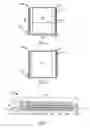
Referring now to FIG. 1, therein is shown a top view of an integrated circuit package system 100 in a first embodiment of the present invention. The top view depicts a top integrated circuit die 102 exposed by an encapsulation 104, such as a cover of an epoxy molding compound. The top integrated circuit die 102 is shown not centered relative to the integrated circuit package system 100, as an example. The encapsulation 104 includes a non-elevated portion 106 and an elevated portion 108. The non-elevated portion 106 exposed a top side 110 of leads 112. The top side 110 of the leads 112 does not extend to the edge of the encapsulation 104, as an example.
For illustrative purposes, the integrated circuit package system 100 is shown with the leads 112 at opposite sides, although it is understood that the integrated circuit package system 100 can have the leads 112 in different configurations. For example, the leads 112 may be along all the sides, some of the sides, or one side of the integrated circuit package system 100. As another example, the integrated circuit package system 100 may have multiple rows of the leads 112.
Referring now to FIG. 2, therein is shown a bottom view of the integrated circuit package system 100 of FIG. 1. The bottom view depicts a bottom integrated circuit die 214 exposed by the encapsulation 104. The bottom integrated circuit die 214 is shown not centered relative to the integrated circuit package system 100, as an example. The encapsulation 104 exposes a bottom side 216 of the leads 112. The bottom side 216 of the leads 112 extends to the edge of the encapsulation 104, as an example.
Referring now to FIG. 3, therein is shown a cross-sectional view of the integrated circuit package system 100 along 3-3 of FIG. 1. The cross-sectional view depicts a bottom non-active side 318 of the bottom integrated circuit die 214 substantially coplanar with the bottom side 216 of the leads 112 and a bottom surface 320 of the encapsulation 104. A top surface 322 of the encapsulation 104 includes the non-elevated portion 106 and the elevated portion 108. The leads 112 include a protrusion 324 having the top side 110 exposed at the non-elevated portion 106 of the encapsulation 104. Sides 326 of the protrusion 324 are surrounded by the encapsulation 104 allowing the leads 112 to function as a mold interlock thereby improving reliability, such as in moisture sensitivity level (MSL) performance.
A first integrated circuit die 328 can be over the bottom integrated circuit die 214 in an offset configuration. An adhesive 330, such as a die-attach adhesive, is between the bottom integrated circuit die 214 and the first integrated circuit die 328. A second integrated circuit die 332 can be over the first integrated circuit die 328 in an offset configuration in a similar direction to the bottom integrated circuit die 214. A third integrated circuit die 334 can be over the second integrated circuit die 332 in an offset configuration in a similar direction to the first integrated circuit die 328. The top integrated circuit die 102 can be over the third integrated circuit die 334.
The adhesive 330 is also between the first integrated circuit die 328 and the second integrated circuit die 332, the second integrated circuit die 332 and the third integrated circuit die 334, and the third integrated circuit die 334 and the top integrated circuit die 102. Internal interconnects 336, such as bond wires or ribbon bond wires, connect the bottom integrated circuit die 214, the first integrated circuit die 328, the second integrated circuit die 332, and the third integrated circuit die 334 with the leads 112.
The encapsulation 104 covers an integrated circuit stack 338 of the bottom integrated circuit die 214, the first integrated circuit die 328, the second integrated circuit die 332, the third integrated circuit die 334, and the top integrated circuit die 102 with the bottom non-active side 318 and a top non-active side 340 of the top integrated circuit die 102 exposed. The encapsulation 104 also covers the internal interconnects 336 and the leads 112 with the top side 110 and the bottom side 216 exposed. The elevated portion 108 of the encapsulation 104 is above the height of the protrusion 324 of the leads 112.
The integrated circuit stack 338 can serve to provide mechanical rigidity for the integrated circuit package system 100. The offset configuration of the integrated circuit stack 338 may also function as a mold interlock for the integrated circuit package system 100.
For illustrative purposes, the integrated circuit stack 338 includes an offset configuration of the integrated circuit dice such that the integrated circuit dice or the adhesive 330 do not interfere with the connections of the internal interconnects 336, although it is understood that the bottom integrated circuit die 214, the first integrated circuit die 328, the integrated circuit stack 338 may be stacked differently. For example, the integrated circuit stack 338 can include a spacer, such as a wire-in-film, as the adhesive 330 within the integrated circuit stack 338 allowing the internal interconnects 336 to connect to one or more of the integrated circuit dice within the spacer.
Also for illustrative purposes, the integrated circuit package system 100 is shown with the top integrated circuit die 102, although it is understood that the integrated circuit package system 100 can have a different structure. For example, the top integrated circuit die 102 can represent a dummy semiconductor structure that is not an integrated circuit for providing clearance of the internal interconnects 336 attached with the third integrated circuit die 334 and for providing structural support to resist warpage.
Referring now to FIG. 4, therein is shown a top view of an integrated circuit package system 400 in a second embodiment of the present invention. The top view depicts a top integrated circuit die 402 exposed by an encapsulation 404, such as a cover of an epoxy molding compound. The top integrated circuit die 402 is shown not centered relative to the integrated circuit package system 400, as an example. The encapsulation 404 includes a non-elevated portion 406 and an elevated portion 408. The non-elevated portion 406 exposed a top side 410 of leads 412. The leads 412 extend to the edge of the encapsulation 404, as an example.
For illustrative purposes, the integrated circuit package system 400 is shown with the leads 412 at opposite sides, although it is understood that the integrated circuit package system 400 can have the leads 412 in different configurations. For example, the leads 412 may be along all the sides, some of the sides, or one side of the integrated circuit package system 400. As another example, the integrated circuit package system 400 may have multiple rows of the leads 412.
Referring now to FIG. 5, therein is shown a bottom view of the integrated circuit package system 400 of FIG. 4. The bottom view depicts a bottom integrated circuit die 514 exposed by the encapsulation 404. The bottom integrated circuit die 514 is shown not centered relative to the integrated circuit package system 400, as an example. The encapsulation 404 exposes a bottom side 516 of the leads 412.
Referring now to FIG. 6, therein is shown a cross-sectional view of the integrated circuit package system 400 along 6-6 of FIG. 4. The cross-sectional view depicts a bottom non-active side 518 of the bottom integrated circuit die 514 substantially coplanar with the bottom side 516 of the leads 412 and a bottom surface 520 of the encapsulation 404. A top surface 522 of the encapsulation 404 includes the non-elevated portion 406 and the elevated portion 408. The top side 410 of the leads 412 is also shown as coplanar with the non-elevated portion 406 of the encapsulation 404, as an example.
A first integrated circuit die 528 can be over the bottom integrated circuit die 514 in an offset configuration. An adhesive 530, such as a die-attach adhesive, is between the bottom integrated circuit die 514 and the first integrated circuit die 528. A second integrated circuit die 532 can be over the first integrated circuit die 528 in an offset configuration in a similar direction to the bottom integrated circuit die 514. A third integrated circuit die 534 can be over the second integrated circuit die 532 in an offset configuration in a similar direction to the first integrated circuit die 528. The top integrated circuit die 402 can be over the third integrated circuit die 534.
The adhesive 530 is also between the first integrated circuit die 528 and the second integrated circuit die 532, the second integrated circuit die 532 and the third integrated circuit die 534, and the third integrated circuit die 534 and the top integrated circuit die 402. Internal interconnects 536, such as bond wires or ribbon bond wires, connect the bottom integrated circuit die 514, the first integrated circuit die 528, the second integrated circuit die 532, and the third integrated circuit die 534 with the leads 412.
The encapsulation 404 covers an integrated circuit stack 538, wherein the integrated circuit stack 538 includes the bottom integrated circuit die 514, the first integrated circuit die 528, the second integrated circuit die 532, the third integrated circuit die 534, and the top integrated circuit die 402 with the bottom non-active side 518 and a top non-active side 540 of the top integrated circuit die 402 exposed. The encapsulation 404 also covers the internal interconnects 536 and the leads 412 with the top side 410 and the bottom side 516 exposed. The height of the elevated portion 408 of the encapsulation 404 is above the height of a protrusion 524 of the leads 412.
The integrated circuit stack 538 can serve to provide mechanical rigidity for the integrated circuit package system 400. The offset configuration of the integrated circuit stack 538 may also function as a mold interlock for the integrated circuit package system 400.
For illustrative purposes, the integrated circuit stack 538 includes an offset configuration of the integrated circuit dice such that the integrated circuit dice or the adhesive 530 do not interfere with the connections of the internal interconnects 536, although it is understood that the bottom integrated circuit die 514, the first integrated circuit die 528, the integrated circuit stack 538 may be stacked differently. For example, the integrated circuit stack 538 can include a spacer, such as a wire-in-film, as the adhesive 530 within the integrated circuit stack 538 allowing the internal interconnects 536 to connect to one or more of the integrated circuit dice within the spacer.
Referring now to FIG. 7, therein is shown a cross-sectional view of an integrated circuit package system 700 in a third embodiment of the present invention. The integrated circuit package system 700 is an integrated circuit package-in-package system with a stack having the integrated circuit package system 100 mounted over a carrier 742, such as a substrate.
The elevated portion 108 of the encapsulation 104 functions as a spacer allowing package interconnects 744, such as bond wires or ribbon bond wires, to connect to the top side 110 of the leads 112 and the carrier 742. This eliminates the need for separate or discrete spacer structures thereby reducing manufacturing complexity, reducing the package profile, and lowering cost.
A package encapsulation 746, such as a cover of an epoxy molding compound, covers the stack of the integrated circuit package system 100 and the package interconnects 744 over the carrier 742. External interconnects 748, such as solder balls, can attach to the bottom of the carrier 742 for connection to the next system level (not shown), such as a printed circuit board or another integrated circuit package system.
For illustrative purposes, the integrated circuit package system 100 adjacent to the carrier 742 is shown connected to the carrier 742 with the package interconnects 744, although it is understood that the integrated circuit package system 100 may be connected to the carrier 742 differently. For example, conductive paste (not shown), such as solder paste, may be used to connect the bottom side 216 of the leads 112 and the carrier 742 or in combination with the package interconnects 744.
Referring now to FIG. 8, therein is shown a cross-sectional view of an integrated circuit package system 800 in a fourth embodiment of the present invention. The integrated circuit package system 800 is an integrated circuit package-in-package system with a stack having the integrated circuit package system 400 mounted over a carrier 842, such as a substrate.
The elevated portion 408 of the encapsulation 404 functions as a spacer allowing package interconnects 844, such as bond wires or ribbon bond wires, to connect to the top side 410 of the leads 412 and the carrier 842. This eliminates the need for separate or discrete spacer structures thereby reducing manufacturing complexity, reducing the package profile, and lowering cost.
A package encapsulation 846, such as a cover of an epoxy molding compound, covers the stack of the integrated circuit package system 400 and the package interconnects 844 over the carrier 842. External interconnects 848, such as solder balls, can attach to the bottom of the carrier 842 for connection to the next system level (not shown), such as a printed circuit board or another integrated circuit package system.
For illustrative purposes, the lower of the integrated circuit package system 400 is shown connected to the carrier 842 with the package interconnects 844, although it is understood that the integrated circuit package system 400 may be connected to the carrier 842 differently. For example, conductive paste (not shown), such as solder paste, may be used to connect the bottom side 516 of the leads 412 and the carrier 842 or in combination with the package interconnects 844.
Referring now to FIG. 9, therein is shown a cross-sectional view of a portion of a lead frame 902 in a die attaching step of a portion the integrated circuit stack 338 of FIG. 3. The cross-sectional view depicts the leads 112 as part of the lead frame 902 and attached with a mounting structure 904, such as a coverlay tape.
A portion of the integrated circuit stack 338 can be formed between the leads 112 with the bottom non-active side 318 of the bottom integrated circuit die 214 attached with the mounting structure 904. The first integrated circuit die 328 mounts over the bottom integrated circuit die 214 in an offset configuration.
Referring now to FIG. 10, therein is shown the structure of FIG. 9 in a connecting step of the internal interconnects 336. The internal interconnects 336 attach between the leads 112 and the bottom integrated circuit die 214. The internal interconnects 336 also attach between the leads 112 and the first integrated circuit die 328.
The second integrated circuit die 332 mounts over the first integrated circuit die 328 in an offset configuration in a similar direction to the bottom integrated circuit die 214. The third integrated circuit die 334 mounts over the second integrated circuit die 332 in an offset configuration in a similar direction to the first integrated circuit die 328. The top integrated circuit die 102 mounts over the third integrated circuit die 334. The adhesive 330 is between the integrated circuit dice in the integrated circuit stack 338. The top non-active side 340 of the top integrated circuit die 102 faces away from the mounting structure 904.
The internal interconnects 336 continue to attach between the leads 112 and both the second integrated circuit die 332 and the third integrated circuit die 334 in the integrated circuit stack 338. The offset configuration of the integrated circuit dice in the integrated circuit stack 338 provides clearance for the connection of the internal interconnects 336 with the integrated circuit stack 338.
Referring now to FIG. 11, therein is shown the structure of FIG. 10 in a forming step of the encapsulation 104. The cross-sectional view depicts portions of adjacent structures of FIG. 10 with the leads 112 still attached to each other from the adjacent structures in the lead frame 902. The encapsulation 104 is formed surrounding the internal interconnects 336 and the integrated circuit stack 338 in each of the adjacent structures. The top non-active side 340 and the bottom non-active side 318 are exposed from the encapsulation 104. The encapsulation 104 also exposes the top side 110 and the bottom side 216 of the leads 112.
The mounting structure 904 of FIG. 9 is removed from the encapsulated structure. The encapsulated structure can undergo post molding cure. The encapsulated structure can optionally be plated, such as with copper alloy, nickel/palladium, or gold alloy, and can undergo device marking.
Referring now to FIG. 12, therein is shown the structure of FIG. 11 in a singulating step of the integrated circuit package system 100 of FIG. 3. A singulation element 1202, such as a saw, may cut the leads 112 that are attached without cutting the protrusion 324 forming the integrated circuit package system 100.
Referring now to FIG. 13, therein is shown a flow chart of an integrated circuit package system 1300 for manufacturing of the integrated circuit package system 100 in an embodiment of the present invention. The system 1300 includes forming an integrated circuit stack having a bottom non-active side and a top non-active side in a block 1302; connecting an internal interconnect between a lead, having a top side and a bottom side, and the integrated circuit stack in a block 1304; and forming an encapsulation, having both an non-elevated portion and an elevated portion, around the integrated circuit stack and the internal interconnect with the top side exposed at the non-elevated portion, and with the bottom side, the bottom non-active side, and the top non-active side exposed in a block 1306.
These and other valuable aspects of the present invention consequently further the state of the technology to at least the next level.
Thus, it has been discovered that the integrated circuit package-on-package stacking system of the present invention furnishes important and heretofore unknown and unavailable solutions, capabilities, and functional aspects for developing and manufacturing package-on-package stacked solutions. The resulting processes and configurations are straightforward, cost-effective, uncomplicated, highly versatile, and effective, can be surprisingly and unobviously implemented by adapting known technologies, and are thus readily suited for efficiently and economically manufacturing package-on-package stacked devices fully compatible with conventional manufacturing processes and technologies. The resulting processes and configurations are straightforward, cost-effective, uncomplicated, highly versatile, accurate, sensitive, and effective, and can be implemented by adapting known components for ready, efficient, and economical manufacturing, application, and utilization.
While the invention has been described in conjunction with a specific best mode, it is to be understood that many alternatives, modifications, and variations will be apparent to those skilled in the art in light of the aforegoing description. Accordingly, it is intended to embrace all such alternatives, modifications, and variations that fall within the scope of the included claims. All matters hithertofore set forth herein or shown in the accompanying drawings are to be interpreted in an illustrative and non-limiting sense.
Claims
What is claimed is:1. An integrated circuit package system comprising:
forming an integrated circuit stack having a bottom non-active side and a top non-active side;
connecting an internal interconnect between a lead, having a top side and a bottom side, and the integrated circuit stack; and
forming an encapsulation, having both a non-elevated portion and an elevated portion, around the integrated circuit stack and the internal interconnect with the top side exposed at the non-elevated portion, and with the bottom side, the bottom non-active side, and the top non-active side exposed.
2. The system as claimed in claim 1 wherein forming the encapsulation includes covering a side of a protrusion of the lead with the protrusion including the top side.
3. The system as claimed in claim 1 wherein forming the encapsulation includes forming the elevated portion of the encapsulation above the top side of the lead.
4. The system as claimed in claim 1 wherein forming the integrated circuit stack includes forming the integrated circuit stack having integrated circuit dice in an offset configuration.
5. The system as claimed in claim 1 further comprising:
mounting a further integrated circuit package system over the elevated portion of the encapsulation;
connecting a package interconnect between a carrier and the lead with the package interconnect in a clearance formed by the elevated portion; and
forming a package encapsulation over the further integrated circuit package system, the package interconnect, and the carrier.
6. An integrated circuit package system comprising:
forming an integrated circuit stack, having a bottom non-active side and a top non-active side, with integrated circuit dice in an offset configuration;
connecting an internal interconnect between a lead, having a top side and a bottom side, and the integrated circuit stack; and
forming an encapsulation around the integrated circuit stack and the internal interconnect including:
forming the encapsulation having both an non-elevated portion and an elevated portion,
exposing the top side exposed at the non-elevated portion,
exposing the top non-active side at the elevated portion, and
exposing the bottom side and the bottom non-active side from a bottom surface of the encapsulation.
7. The system as claimed in claim 6 wherein exposing the bottom side and the bottom non-active side at the bottom surface of the encapsulation includes attaching the internal interconnect in a clearance in the offset configuration in the integrated circuit stack.
8. The system as claimed in claim 6 wherein exposing the bottom side and the bottom non-active side at the bottom surface of the encapsulation includes forming the bottom surface coplanar with the bottom side.
9. The system as claimed in claim 6 wherein forming the encapsulation having the elevated portion includes forming the elevated portion above the top side.
10. The system as claimed in claim 6 wherein exposing the top non-active side includes exposing the top non-active side from a top surface of the encapsulation.
11. An integrated circuit package system comprising:
an integrated circuit stack having a bottom non-active side and a top non-active side;
a lead, having a top side and a bottom side, adjacent to the integrated circuit stack;
an internal interconnect between the lead and the integrated circuit stack; and
an encapsulation, having both a non-elevated portion and an elevated portion, around the integrated circuit stack and the internal interconnect with the top side exposed at the non-elevated portion, and with the bottom side, the bottom non-active side, and the top non-active side exposed.
12. The system as claimed in claim 11 wherein the lead includes a protrusion having the top side.
13. The system as claimed in claim 11 wherein the elevated portion of the encapsulation is above the top side of the lead.
14. The system as claimed in claim 11 wherein the integrated circuit stack includes integrated circuit dice in an offset configuration.
15. The system as claimed in claim 11 further comprising:
a carrier;
a further integrated circuit package system over the elevated portion of the encapsulation and the carrier;
a package interconnect between the carrier and the lead with the package interconnect in a clearance formed by the elevated portion; and
a package encapsulation over the further integrated circuit package system, the package interconnect, and the carrier.
16. The system as claimed in claim 11 wherein:
the integrated circuit stack includes integrated circuit dice in an offset configuration;
the top non-active side of the integrated circuit stack is exposed from the elevated portion, and
the bottom side and the bottom non-active side are exposed from a bottom surface of the encapsulation.
17. The system as claimed in claim 16 wherein the internal interconnect is in a clearance in the offset configuration in the integrated circuit stack.
18. The system as claimed in claim 16 wherein the bottom surface of the encapsulation is coplanar with the bottom side.
19. The system as claimed in claim 16 wherein the elevated portion of the encapsulation is above the top side.
20. The system as claimed in claim 16 wherein the top non-active side of the integrated circuit stack is exposed from a top surface of the encapsulation.
Images & Drawings included:


Sources:
- United States Patent and Trademark Office - verify current appl. status at the USPTO↗
Recent applications in this class:
- » 20250293128 2025-09-18
SEMICONDUCTOR DEVICE - » 20250279340 2025-09-04
MULTI-CHIP SEMICONDUCTOR MODULE WITH BALANCED SWITCHING - » 20250273546 2025-08-28
INTEGRATED CIRCUIT PACKAGING WITH INSULATION STRUCTURE TO CONTROL GAP HEIGHT AND DIE TILT - » 20250266335 2025-08-21
SEMICONDUCTOR DEVICE WITH EMBEDDED BATTERY AND METHOD THEREFOR - » 20250253214 2025-08-07
PACKAGE STRUCTURE AND METHOD OF FORMING THEREOF - » 20250253213 2025-08-07
MULTI-DIE ISOLATED LEAD FRAME PACKAGE - » 20250239507 2025-07-24
IC PACKAGE WITH DIE AND COPPER POSTS - » 20250226296 2025-07-10
SEMICONDUCTOR DEVICE AND METHOD FOR MANUFACTURING THE SAME - » 20250226295 2025-07-10
MULTI-DIE SEMICONDUCTOR PACKAGE - » 20250218908 2025-07-03
MULTI-DIE TRANSFORMER POWER MODULES
Recent applications for this Assignee:
- » 20160351486 2016-12-01
Semiconductor device and method of forming substrate including embedded component with symmetrical structure - » 20160300817 2016-10-13
Semiconductor device and method of forming a package in-fan out package - » 20160300797 2016-10-13
Double-sided semiconductor package and dual-mold method of making same - » 20160276307 2016-09-22
Semiconductor device and method of forming PoP semiconductor device with RDL over top package - » 20160276238 2016-09-22
Semiconductor device and method of forming supporting layer over semiconductor die in thin fan-out wafer level chip scale package - » 20160233168 2016-08-11
Semiconductor device and method of forming 3D dual side die embedded build-up semiconductor package - » 20160218089 2016-07-28
Semiconductor device and method of forming WLCSP with semiconductor die embedded within interconnect structure - » 20160214857 2016-07-28
Semiconductor device and method of forming MEMS package - » 20160197059 2016-07-07
Semiconductor device and method of forming shielding layer over integrated passive device using conductive channels - » 20160197022 2016-07-07
Semiconductor device and method of forming sacrificial adhesive over contact pads of semiconductor die