Touch screen system with light reflection
US20090141006A1
2009-06-04
12/325,209
2008-11-30
✅ Patent granted
US 8,289,297 B2
2012-10-16
-
-
Quan-Zhen Wang | Yuk Chow
2031-06-19
Abstract:
The present invention discloses a touch screen system comprising LED infrared transceivers installed at appropriate positions on left and right sides of the screen respectively, and a transmitter end of the transceiver transmits LED infrared waves and spreads spherical waves all over the surface of the screen. If the surface of the screen receives an intrusion from a touch control element, the spherical waves will be interfered, interrupted and reflected, and the wave frequency of the reflection will be detected by the receiver end of the transceiver. After the receiver end has received a reflection signal, the position coordinates of the touch control element can be analyzed through the operation of a core logical unit. A display module is provided for showing the movement path of the touch control element in images or lines, so as to provide a touch screen with low manufacturing cost and long life expectancy.
Inventors:
- Wen-Pin Weng 3 🇹🇼 Taipei, Taiwan
- Weng Wen-Pen 1 🇹🇼 Taipei, Taiwan
- Ko Wen Hui 1 🇹🇼 Chong-Ho City, Taiwan
- Wen Hui Ko 1 🇹🇼 Chong-Ho, Taiwan
Assignee:
- Lunghwa University of Science and Technolgy 1 🇹🇼 Taoyuan, Taiwan
- Lunghwa University of Science and Technology 1 🇹🇼 , Taiwan
Interested in similar patents?
Get notified when new applications in this technology area are published.
Classification:
H01L23/13 » CPC main
Details of semiconductor or other solid state devices; Mountings, e.g. non-detachable insulating substrates characterised by the shape
H01L23/49816 » CPC further
Details of semiconductor or other solid state devices; Arrangements for conducting electric current to or from the solid state body in operation, e.g. leads, terminal arrangements ; Selection of materials therefor consisting of soldered constructions; Leads, on insulating substrates,; Additional leads joined to the metallisation on the insulating substrate, e.g. pins, bumps, wires, flat leads Spherical bumps on the substrate for external connection, e.g. ball grid arrays [BGA]
H01L23/49827 » CPC further
Details of semiconductor or other solid state devices; Arrangements for conducting electric current to or from the solid state body in operation, e.g. leads, terminal arrangements ; Selection of materials therefor consisting of soldered constructions; Leads, on insulating substrates, Via connections through the substrates, e.g. pins going through the substrate, coaxial cables
H01L24/49 » CPC further
Arrangements for connecting or disconnecting semiconductor or solid-state bodies; Methods or apparatus related thereto; Means for bonding being attached to, or being formed on, the surface to be connected, e.g. chip-to-package, die-attach, "first-level" interconnects; Manufacturing methods related thereto; Wire connectors; Manufacturing methods related thereto; Structure, shape, material or disposition of the wire connectors after the connecting process of a plurality of wire connectors
H01L24/05 » CPC further
Arrangements for connecting or disconnecting semiconductor or solid-state bodies; Methods or apparatus related thereto; Means for bonding being attached to, or being formed on, the surface to be connected, e.g. chip-to-package, die-attach, "first-level" interconnects; Manufacturing methods related thereto; Bonding areas ; Manufacturing methods related thereto; Structure, shape, material or disposition of the bonding areas prior to the connecting process of an individual bonding area
H01L24/45 » CPC further
Arrangements for connecting or disconnecting semiconductor or solid-state bodies; Methods or apparatus related thereto; Means for bonding being attached to, or being formed on, the surface to be connected, e.g. chip-to-package, die-attach, "first-level" interconnects; Manufacturing methods related thereto; Wire connectors; Manufacturing methods related thereto; Structure, shape, material or disposition of the wire connectors prior to the connecting process of an individual wire connector
H01L24/48 » CPC further
Arrangements for connecting or disconnecting semiconductor or solid-state bodies; Methods or apparatus related thereto; Means for bonding being attached to, or being formed on, the surface to be connected, e.g. chip-to-package, die-attach, "first-level" interconnects; Manufacturing methods related thereto; Wire connectors; Manufacturing methods related thereto; Structure, shape, material or disposition of the wire connectors after the connecting process of an individual wire connector
H01L2224/05573 » CPC further
Indexing scheme for arrangements for connecting or disconnecting semiconductor or solid-state bodies and methods related thereto as covered by; Means for bonding being attached to, or being formed on, the surface to be connected, e.g. chip-to-package, die-attach, "first-level" interconnects; Manufacturing methods related thereto; Bonding areas; Manufacturing methods related thereto; Structure, shape, material or disposition of the bonding areas prior to the connecting process of an individual bonding area; External layer Single external layer
H01L2224/16 » CPC further
Indexing scheme for arrangements for connecting or disconnecting semiconductor or solid-state bodies and methods related thereto as covered by; Means for bonding being attached to, or being formed on, the surface to be connected, e.g. chip-to-package, die-attach, "first-level" interconnects; Manufacturing methods related thereto; Bump connectors; Manufacturing methods related thereto; Structure, shape, material or disposition of the bump connectors after the connecting process of an individual bump connector
H01L2224/4911 » CPC further
Indexing scheme for arrangements for connecting or disconnecting semiconductor or solid-state bodies and methods related thereto as covered by; Means for bonding being attached to, or being formed on, the surface to be connected, e.g. chip-to-package, die-attach, "first-level" interconnects; Manufacturing methods related thereto; Wire connectors; Manufacturing methods related thereto; Structure, shape, material or disposition of the wire connectors after the connecting process of a plurality of wire connectors; Disposition the connectors being bonded to at least one common bonding area, e.g. daisy chain
H01L2924/01005 » CPC further
Indexing scheme for arrangements or methods for connecting or disconnecting semiconductor or solid-state bodies as covered by; Chemical elements Boron [B]
H01L2924/01033 » CPC further
Indexing scheme for arrangements or methods for connecting or disconnecting semiconductor or solid-state bodies as covered by; Chemical elements Arsenic [As]
H01L2924/01082 » CPC further
Indexing scheme for arrangements or methods for connecting or disconnecting semiconductor or solid-state bodies as covered by; Chemical elements Lead [Pb]
H01L2924/014 » CPC further
Indexing scheme for arrangements or methods for connecting or disconnecting semiconductor or solid-state bodies as covered by; Alloys Solder alloys
H01L2924/19107 » CPC further
Indexing scheme for arrangements or methods for connecting or disconnecting semiconductor or solid-state bodies as covered by; Details of hybrid assemblies other than the semiconductor or other solid state devices to be connected; Disposition of discrete passive components off-chip wires
H01L2924/30105 » CPC further
Indexing scheme for arrangements or methods for connecting or disconnecting semiconductor or solid-state bodies as covered by; Technical effects; Electrical effects Capacitance
H01L2224/73215 » CPC further
Indexing scheme for arrangements for connecting or disconnecting semiconductor or solid-state bodies and methods related thereto as covered by; Means for bonding being of different types provided for in two or more of groups; Location after the connecting process on the same surface Layer and wire connectors
H01L2924/12041 » CPC further
Indexing scheme for arrangements or methods for connecting or disconnecting semiconductor or solid-state bodies as covered by; Details of semiconductor or other solid state devices to be connected; Device type; Passive devices, e.g. 2 terminal devices; Optical Diode LED
H01L2924/351 » CPC further
Indexing scheme for arrangements or methods for connecting or disconnecting semiconductor or solid-state bodies as covered by; Technical effects; Mechanical effects Thermal stress
H01L2924/181 » CPC further
Indexing scheme for arrangements or methods for connecting or disconnecting semiconductor or solid-state bodies as covered by; Details of package parts other than the semiconductor or other solid state devices to be connected Encapsulation
H01L2924/00012 » CPC further
Indexing scheme for arrangements or methods for connecting or disconnecting semiconductor or solid-state bodies as covered by; Technical content checked by a classifier Relevant to the scope of the group, the symbol of which is combined with the symbol of this group
H01L2924/00014 » CPC further
Indexing scheme for arrangements or methods for connecting or disconnecting semiconductor or solid-state bodies as covered by; Technical content checked by a classifier the subject-matter covered by the group, the symbol of which is combined with the symbol of this group, being disclosed without further technical details
H01L2924/15311 » CPC further
Indexing scheme for arrangements or methods for connecting or disconnecting semiconductor or solid-state bodies as covered by; Details of package parts other than the semiconductor or other solid state devices to be connected; Die mounting substrate; Connection portion the connection portion being formed only on the surface of the substrate opposite to the die mounting surface being a ball array, e.g. BGA
H01L2224/73204 » CPC further
Indexing scheme for arrangements for connecting or disconnecting semiconductor or solid-state bodies and methods related thereto as covered by; Means for bonding being of different types provided for in two or more of groups; Location after the connecting process on the same surface; Bump and layer connectors the bump connector being embedded into the layer connector
H01L2924/00 » CPC further
Indexing scheme for arrangements or methods for connecting or disconnecting semiconductor or solid-state bodies as covered by
G06F3/042 IPC
Input arrangements for transferring data to be processed into a form capable of being handled by the computer; Output arrangements for transferring data from processing unit to output unit, e.g. interface arrangements; Input arrangements or combined input and output arrangements for interaction between user and computer; Arrangements for converting the position or the displacement of a member into a coded form; Digitisers, e.g. for touch screens or touch pads, characterised by the transducing means by opto-electronic means
Description
This application is a Continuation-In-Part of my patent application, Ser. No. 12/258,466, filed on Oct. 27, 2008.
FIELD OF THE INVENTION
The present invention generally relates to touch screens, and more particularly to a touch screen system wherein the light emitting diode (LED) infrared waves is reflection interrupted.
BACKGROUND OF THE INVENTION
In a traditional touch screen, a sensor generally comes with a digital capacitance structure having two sensing layers installed at the top and bottom of a touch screen panel respectively and coupled to a control circuit, such that a capacitance effect is produced instantaneously when a user touches the touch screen panel by a finger or a conductor. However, such arrangement of using the change of capacitance to determine the position of the user's finger or the conductor exert stresses repeatedly on the touch screen panel, and this design has the drawback of deforming or damaging the touch screen panel easily.
Later, manufacturers developed a touch screen that measures and determines the user's finger or the conductor by blocking infrared light, but such design requires a large number of touch control elements arranged linearly or in rows on the screen for one-to-one transmission and receiving. Obviously, this design has the drawback of incurring a higher cost.
To overcome the shortcomings of the prior art, the inventor of the present invention, based on years of experience in the related industry. develops a touch screen system that reflects and interrupts the LED infrared waves.
SUMMARY OF THE INVENTION
Therefore, it is a primary objective of the present invention to provide a touch screen system with light reflection, and the touch screen system comprises an LED infrared transceivers installed at appropriate positions on both left and right sides of the screen respectively, and a transmitter end of the transceiver transmits LED infrared waves and spreads spherical waves all over the surface of the screen, such that if the surface of the screen receives an intrusion from the touch control element, the spherical waves will be interfered, interrupted and reflected, and the wave frequency of the reflection will be detected by the receiver end of the transceiver. After the receiver end has received a reflection signal, the position coordinates of the touch control element can be analyzed through the operation of a core logical unit. In addition to the advantages of low manufacturing cost and fast signal transmission, the present invention also overcomes the aforementioned shortcoming of the traditional capacitance type touch screen being deformed or damaged easily by repeated exertions of stress to enhance the life and popularity of the touch screen.
BRIEF DESCRIPTION OF THE DRAWINGS
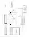
FIG. 1 shows a schematic diagram of a touch screen system with light reflection in accordance with a preferred embodiment of the present invention; and
FIG. 2 shows a schematic diagram of a touch screen system with light reflection in accordance with another preferred embodiment of the present invention.
DETAILED DESCRIPTION OF PREFERRED EMBODIMENTS
With reference to FIG. 1, a touch screen system in accordance with a preferred embodiment of the present invention comprises a screen 1 and an LED infrared transceiver 11 disposed separately at appropriate positions on both sides of the screen 1 and having a transmitter end 111 and a receiver 112 for transmitting and receiving LED infrared waves respectively. The LED infrared waves transmitted from the transmitters 111 on both sides form spherical waves all over the entire screen 1 to constitute an image signal detection net, such that if a touch control element 13 intrudes the image signal detection net, the LED infrared waves will be interrupted and reflected, and the receiver end 112 will be able to receive the reflected waves to capture target images and transmit the target images to an LED infrared image signal capture circuit 2 electrically coupled to the receiver end 112. After going through a noise filter 3, the target images are transmitted to an image analysis circuit 4, and a core logical operation 41 is provided for comparing two target images and computing the positions of the touch control element 13 corresponding to the two target images on the screen 1.
In the aforementioned core logical operation, there is a time difference between the moment of transmitting a light wave from the transmitter end 111 to touch the touch control element 13 and the moment of receipt of the light wave by the receiver end 112. The time difference is multiplied by the speed of light to obtain the distance between the touch control element 13 and the LED infrared transceiver 11. The mediate point between the transmitter end 111 and the receiver end 112 is used as the center and the distance is used as a radius to form a quarter circle. The LED infrared transceivers 11 on both sides form their respective quarter circuits by the same way. The intersection point of the two quarter circles formed on the screen 1 is processed to indicate the position coordinates of the touch control element 13 on the screen 1.
With reference to FIG. 2, a touch screen system in accordance with a second preferred embodiment of the present invention comprises a transmitter end 111 and a receiver end 112, both of which are originally installed in a same component in the first embodiment, and are installed at different positions on the screen 1 in the second embodiment, wherein the two transmitter ends 111 and two receiver ends 112 are installed diagonally with each other. In other words, each transmitter end 111 and each receiver end 112 are installed on the same side, and two diagonally installed transmitter ends 111 can transmit LED infrared waves to spread spherical waves all over the screen 1. If a touch control element 13 intrudes the spherical waves to interrupt the wavelength, a reflection will be formed by the interrupted wavelength and detected by the receiver end 112 to form a target signal. The target signal is transmitted to the LED infrared image signal capture circuit 2 electrically coupled to the receiver end 112. After going through the noise filter 3, the target signal is transmitted to the image analysis circuit 4. The core logical operation is provided to compare two target signals and calculate the position of the touch control element 13 corresponding to the two target images.
The aforementioned core logical operation method is the same as the one illustrated in FIG. 1, wherein there is also a time difference between the moment of transmitting a light wave from the transmitter end 111 to touch the touch control element 13 and the moment of receipt of the light wave by the receiver end 112. The time difference is multiplied by the speed of light to obtain the distance between the touch control element 13 and the LED infrared transceiver 11. The mediate point between the transmitter end 111 and the receiver end 112 is used as the center and the distance obtained is used as a radius to form a quarter circle. The intersection point of the two quarter circles formed on the screen 1 indicates the position coordinates of the touch control element 13 on the screen 1.
While we have shown and described the embodiment in accordance with the present invention, it should be clear to those skilled in the art that further embodiments may be made without departing from the scope of the present invention.
Claims
What is claimed is:1. A touch screen system, comprising:
a screen;
at least one light emitting diode (LED) infrared transceiver, disposed at a position of the screen;
an LED infrared image signal capture circuit electrically coupled to the LED infrared transceiver for capturing a target image detected by a receiver end of the LED infrared transceiver; and
an image analysis circuit electrically coupled to the LED infrared image signal capture circuit so as to compute the target image by a computation method to determine the position of a touch control element on the screen.
2. The touch screen system of claim 1, further comprising a noise filter electrically coupled between the LED infrared image signal capture circuit and the image analysis circuit.
3. The touch screen system of claim 1, wherein the computation method obtains a distance by multiplying the time difference between the transmission and receipt of the light waves with the speed of light, and uses the mediate point between the transmitter end and the receiver end as a center and the computed distance as a radius to form a quarter circle, a intersection point of the two quarter circles indicates the position coordinates of the touch control element on the screen.
4. The touch screen system of claim 1, wherein the transmitter end and the receiver end of the LED infrared transceiver are disposed in a same component or disposed separately in different components.
5. The touch screen system of claim 4, wherein the separately disposed transmitter end and receiver end are installed diagonally with respect to each other.
Images & Drawings included:


Sources:
- United States Patent and Trademark Office - verify current appl. status at the USPTO↗
Similar patent applications:
- » 20100238138
Optical touch screen systems using reflected light
Recent applications in this class:
- » 20250273522 2025-08-28
PACKAGE COMPRISING A SUBSTRATE INCLUDING A VIA INTERCONNECT WITH A PARTIAL CONCENTRIC PLANAR CROSS SECTION - » 20250266309 2025-08-21
Method for manufacturing semiconductor structure - » 20250253197 2025-08-07
CHIP PACKAGE STRUCTURE AND MANUFACTURING METHOD THEREOF - » 20250246489 2025-07-31
PACKAGE STRUCTURE - » 20250233030 2025-07-17
SEMICONDUCTOR MODULE - » 20250226273 2025-07-10
MULTILAYER SUBSTRATES AND METHODS FOR MANUFACTURING SAME, POWER MODULES AND METHODS FOR MANUFACTURING SAME, AND ELECTRICAL SYSTEMS - » 20250226272 2025-07-10
SEMICONDUCTOR PACKAGE WITH A BLOCKING ELEMENT FORMED ON A SURFACE OF AN INSULATING LAYER - » 20250218879 2025-07-03
RESIST TENTING AND PLATING IN CORE CAVITY FOR COMPONENT ATTACHMENT - » 20250210424 2025-06-26
SEMICONDUCTOR DEVICE AND METHOD FOR MANUFACTURING SEMICONDUCTOR DEVICE - » 20250210423 2025-06-26
PLATE SHAPED SUBSTRATE AND PACKAGING SUBSTRATE