Semiconductor device
US20100007003A1
2010-01-14
12/260,494
2008-10-29
✅ Patent granted
US 7,719,087 B2
2010-05-18
-
-
Hsien-ming Lee
2029-01-07
Abstract:
A semiconductor device includes: a GaAs chip; and a resin sealing the GaAs chip. The GaAs chip includes: a p-type GaAs layer; an n-type GaAs layer on the p-type GaAs layer; a metal electrode located on the n-type GaAs layer along an edge of the GaAs chip and to which a positive voltage is applied; a device region located in a central portion of the GaAs chip; a semi-insulating region located between the metal electrode and the device region and extending in the p-type GaAs layer and the n-type GaAs layer; and a connecting portion disposed outside the semi-insulating region and electrically connecting the p-type GaAs layer to the metal electrode.
Assignee:
- MITSUBISHI ELECTRIC CORPORATION 16,560 🇯🇵 TOKYO, Japan
Interested in similar patents?
Get notified when new applications in this technology area are published.
Classification:
H01L2224/04042 » CPC further
Indexing scheme for arrangements for connecting or disconnecting semiconductor or solid-state bodies and methods related thereto as covered by; Means for bonding being attached to, or being formed on, the surface to be connected, e.g. chip-to-package, die-attach, "first-level" interconnects; Manufacturing methods related thereto; Bonding areas; Manufacturing methods related thereto; Structure, shape, material or disposition of the bonding areas prior to the connecting process Bonding areas specifically adapted for wire connectors, e.g. wirebond pads
H01L29/0657 » CPC main
Semiconductor devices adapted for rectifying, amplifying, oscillating or switching, or capacitors or resistors with at least one potential-jump barrier or surface barrier, e.g. PN junction depletion layer or carrier concentration layer; Details of semiconductor bodies or of electrodes thereof; Multistep manufacturing processes therefor; Semiconductor bodies ; Multistep manufacturing processes therefor characterised by their shape; characterised by the shapes, relative sizes, or dispositions of the semiconductor regions ; characterised by the concentration or distribution of impurities within semiconductor regions characterised by the shape of the body
H01L23/3185 » CPC further
Details of semiconductor or other solid state devices; Encapsulations, e.g. encapsulating layers, coatings, e.g. for protection characterised by the arrangement or shape; Partial encapsulation or coating the coating covering also the sidewalls of the semiconductor body
H01L23/564 » CPC further
Details of semiconductor or other solid state devices Details not otherwise provided for, e.g. protection against moisture
H01L24/05 » CPC further
Arrangements for connecting or disconnecting semiconductor or solid-state bodies; Methods or apparatus related thereto; Means for bonding being attached to, or being formed on, the surface to be connected, e.g. chip-to-package, die-attach, "first-level" interconnects; Manufacturing methods related thereto; Bonding areas ; Manufacturing methods related thereto; Structure, shape, material or disposition of the bonding areas prior to the connecting process of an individual bonding area
H01L24/48 » CPC further
Arrangements for connecting or disconnecting semiconductor or solid-state bodies; Methods or apparatus related thereto; Means for bonding being attached to, or being formed on, the surface to be connected, e.g. chip-to-package, die-attach, "first-level" interconnects; Manufacturing methods related thereto; Wire connectors; Manufacturing methods related thereto; Structure, shape, material or disposition of the wire connectors after the connecting process of an individual wire connector
H01L23/3121 » CPC further
Details of semiconductor or other solid state devices; Encapsulations, e.g. encapsulating layers, coatings, e.g. for protection characterised by the arrangement or shape the device being completely enclosed a substrate forming part of the encapsulation
H01L24/45 » CPC further
Arrangements for connecting or disconnecting semiconductor or solid-state bodies; Methods or apparatus related thereto; Means for bonding being attached to, or being formed on, the surface to be connected, e.g. chip-to-package, die-attach, "first-level" interconnects; Manufacturing methods related thereto; Wire connectors; Manufacturing methods related thereto; Structure, shape, material or disposition of the wire connectors prior to the connecting process of an individual wire connector
H01L24/49 » CPC further
Arrangements for connecting or disconnecting semiconductor or solid-state bodies; Methods or apparatus related thereto; Means for bonding being attached to, or being formed on, the surface to be connected, e.g. chip-to-package, die-attach, "first-level" interconnects; Manufacturing methods related thereto; Wire connectors; Manufacturing methods related thereto; Structure, shape, material or disposition of the wire connectors after the connecting process of a plurality of wire connectors
H01L24/73 » CPC further
Arrangements for connecting or disconnecting semiconductor or solid-state bodies; Methods or apparatus related thereto Means for bonding being of different types provided for in two or more of groups , , , , , , ,
H01L2924/01005 » CPC further
Indexing scheme for arrangements or methods for connecting or disconnecting semiconductor or solid-state bodies as covered by; Chemical elements Boron [B]
H01L2924/01006 » CPC further
Indexing scheme for arrangements or methods for connecting or disconnecting semiconductor or solid-state bodies as covered by; Chemical elements Carbon [C]
H01L2924/01033 » CPC further
Indexing scheme for arrangements or methods for connecting or disconnecting semiconductor or solid-state bodies as covered by; Chemical elements Arsenic [As]
H01L2924/01079 » CPC further
Indexing scheme for arrangements or methods for connecting or disconnecting semiconductor or solid-state bodies as covered by; Chemical elements Gold [Au]
H01L2924/10329 » CPC further
Indexing scheme for arrangements or methods for connecting or disconnecting semiconductor or solid-state bodies as covered by; Details of semiconductor or other solid state devices to be connected; Material of the semiconductor or solid state bodies; Semiconducting materials; Compound semiconductors; III-V Gallium arsenide [GaAs]
H01L2924/15153 » CPC further
Indexing scheme for arrangements or methods for connecting or disconnecting semiconductor or solid-state bodies as covered by; Details of package parts other than the semiconductor or other solid state devices to be connected; Die mounting substrate; Shape the die mounting substrate comprising a recess for hosting the device
H01L2924/15165 » CPC further
Indexing scheme for arrangements or methods for connecting or disconnecting semiconductor or solid-state bodies as covered by; Details of package parts other than the semiconductor or other solid state devices to be connected; Die mounting substrate Monolayer substrate
H01L2924/00014 » CPC further
Indexing scheme for arrangements or methods for connecting or disconnecting semiconductor or solid-state bodies as covered by; Technical content checked by a classifier the subject-matter covered by the group, the symbol of which is combined with the symbol of this group, being disclosed without further technical details
H01L2224/73265 » CPC further
Indexing scheme for arrangements for connecting or disconnecting semiconductor or solid-state bodies and methods related thereto as covered by; Means for bonding being of different types provided for in two or more of groups; Location after the connecting process on different surfaces Layer and wire connectors
H01L2924/00012 » CPC further
Indexing scheme for arrangements or methods for connecting or disconnecting semiconductor or solid-state bodies as covered by; Technical content checked by a classifier Relevant to the scope of the group, the symbol of which is combined with the symbol of this group
H01L2924/12041 » CPC further
Indexing scheme for arrangements or methods for connecting or disconnecting semiconductor or solid-state bodies as covered by; Details of semiconductor or other solid state devices to be connected; Device type; Passive devices, e.g. 2 terminal devices; Optical Diode LED
H01L2924/1306 » CPC further
Indexing scheme for arrangements or methods for connecting or disconnecting semiconductor or solid-state bodies as covered by; Details of semiconductor or other solid state devices to be connected; Device type; Discrete devices, e.g. 3 terminal devices; Transistor Field-effect transistor [FET]
H01L2924/1305 » CPC further
Indexing scheme for arrangements or methods for connecting or disconnecting semiconductor or solid-state bodies as covered by; Details of semiconductor or other solid state devices to be connected; Device type; Discrete devices, e.g. 3 terminal devices; Transistor Bipolar Junction Transistor [BJT]
H01L2924/12036 » CPC further
Indexing scheme for arrangements or methods for connecting or disconnecting semiconductor or solid-state bodies as covered by; Details of semiconductor or other solid state devices to be connected; Device type; Passive devices, e.g. 2 terminal devices; Rectifying Diode PN diode
H01L2924/00 » CPC further
Indexing scheme for arrangements or methods for connecting or disconnecting semiconductor or solid-state bodies as covered by
H01L23/48 IPC
Details of semiconductor or other solid state devices Arrangements for conducting electric current to or from the solid state body in operation, e.g. leads, terminal arrangements ; Selection of materials therefor
H01L27/082 IPC
Devices consisting of a plurality of semiconductor or other solid-state components formed in or on a common substrate including semiconductor components specially adapted for rectifying, oscillating, amplifying or switching and having at least one potential-jump barrier or surface barrier; including integrated passive circuit elements with at least one potential-jump barrier or surface barrier the substrate being a semiconductor body including only semiconductor components of a single kind including bipolar components only
Description
BACKGROUND OF THE INVENTION
1. Field of the Invention
The present invention relates to a semiconductor device in which a GaAs chip is sealed or encapsulated with a resin, and more particularly to a semiconductor device in which such a GaAs chip has improved moisture resistance.
2. Background Art
There have been proposed resin sealed semiconductor devices in which a semiconductor chip is sealed with a resin [see, e.g., Japanese Laid-Open Patent Publication No. 60-167432 (1985)]. An exemplary such resin sealed semiconductor device includes a GaAs chip as the semiconductor chip. Electrodes are formed along the edges of the GaAs chip, and the device region is formed in the central portion of the GaAs chip.
SUMMARY OF THE INVENTION
These resin sealed semiconductor devices are disadvantageous in that, in a high temperature and high humidity environment, moisture tends to penetrate into the inside of the devices through the surface of the resin or along the interface between the resin and the printed circuit board on which the GaAs chip is mounted. It has happened that this penetration of moisture has caused oxidation of the surface of the GaAs chip around the metal electrodes (to which a positive voltage is applied) and around the device region, resulting in degradation and malfunction of the device.
The present invention has been devised to solve the above problems. It is, therefore, an object of the present invention to provide a semiconductor device whose GaAs chip has improved moisture resistance.
According to one aspect of the present invention, a semiconductor device comprises: a GaAs chip; and a resin sealing said GaAs chip; wherein said GaAs chip includes: a p-type GaAs layer; an n-type GaAs layer formed on said p-type GaAs layer; a metal electrode formed on said n-type GaAs layer along an edge of said GaAs chip and having a positive voltage applied thereto; a device region formed in a central portion of said GaAs chip; a semi-insulating region formed between said metal electrode and said device region and extending in said p-type GaAs layer and said n-type GaAs layer; and a connecting portion disposed outside said semi-insulating region and electrically connecting said p-type GaAs layer to said metal electrode.
Thus the present invention enables an increase in the moisture resistance of the GaAs chip of a semiconductor device.
Other and further objects, features and advantages of the invention will appear more fully from the following description.
BRIEF DESCRIPTION OF THE DRAWINGS
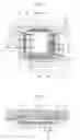
FIG. 1 is a plan view showing the inside of a semiconductor device according to a first embodiment of the present invention.
FIG. 2 is a cross-sectional view taken along line A-A′ of FIG. 1.
FIG. 3 is an enlarged cross-sectional view of an edge portion of the chip shown in FIG. 2.
FIG. 4 shows a comparative semiconductor device.
FIG. 5 is a plan view showing the inside of a semiconductor device according to a second embodiment of the present invention.
FIG. 6 is a cross-sectional view taken along line B-B′ of FIG. 5.
FIG. 7 is an enlarged cross-sectional view of an edge portion of the chip shown in FIG. 6.
DETAILED DESCRIPTION OF THE PREFERRED EMBODIMENTS
First Embodiment
FIG. 1 is a plan view showing the inside of a semiconductor device according to a first embodiment of the present invention.
FIG. 2 is a cross-sectional view taken along line A-A′ of FIG. 1.
Referring to FIGS. 1 and 2, a grounded die pad 12 is provided on a resin or ceramic printed circuit board 10. A GaAs chip 14 with amplifiers, etc. formed therein is bonded onto the die pad 12 by conductive adhesive 16. Metal electrodes 18 are formed along the edges of the GaAs chip 14, and a device region 20 including semiconductor elements, wires, etc. is formed in the central portion of the GaAs chip 14.
The metal electrodes 18 on the GaAs chip 14 are connected by metal wires 24 to electric circuitry 22 provided on the surface of the printed circuit board 10. The GaAs chip 14 is sealed or encapsulated with a resin 26. It should be noted that in order to reduce the required chip area, the metal electrodes 18 are disposed along and near the chip edges, and the device region 20 extends to near the chip edges. The regions 28 of the surface of the GaAs chip 14 are desired to be prevented from oxidation.
FIG. 3 is an enlarged cross-sectional view of an edge portion of the chip shown in FIG. 2. The GaAs chip 14 includes an npn bipolar transistor on a semi-insulating GaAs substrate 30. The npn bipolar transistor includes an n-type GaAs collector layer 32, a p-type GaAs base layer (or simply p-type GaAs layer) 34, and an n-type GaAs emitter layer (or simply n-type GaAs layer) 36 that are sequentially stacked on the semi-insulating GaAs substrate 30. These layers may be formed by epitaxial growth or ion implantation.
The metal electrodes 18 are formed on the n-type GaAs emitter layer 36 along the edges of the GaAs chip 14. A positive voltage is applied to the metal electrodes 18 through the metal wires 24. A semi-insulating region 38 is formed between the metal electrodes 18 and the device region 20 in the central portion of the GaAs chip 14 by ion implantation, and extends through the n-type GaAs collector layer 32, the p-type GaAs base layer 34, and the n-type GaAs emitter layer 36.
According to the present embodiment, a connecting portion 40 is formed outside the semi-insulating region 38 (i.e., near the chip edges), and extends through the n-type GaAs emitter layer 36 to electrically connect the p-type GaAs base layer 34 to the metal electrodes 18.
The advantages of the semiconductor device of the present embodiment will be described by comparing it with the comparative semiconductor device shown in FIG. 4. The comparative semiconductor device does not include the connecting portion 40 of the present embodiment.
Referring to FIG. 4, in a high temperature and high humidity environment, moisture penetrates into the interior of the semiconductor device through the surface of the resin 26 or along the interface between the resin 26 and the printed circuit board 10, and becomes a solution or solvent containing impurities. As a result, the following cathodic reaction is considered to occur at the grounded die pad 12 due to water ionization:
O2+2H2O+4e−→40H−
Further, GaAs has higher ionization tendency than the metal materials, such as Au, used to form the metal electrodes 18 and the wires in the device region 20. Therefore in the case of the comparative semiconductor device, the following anodic reaction is considered to occur at the surface of GaAs chip 14 around the metal electrodes 18 (to which a positive voltage is applied) and around the device region 20:
GaAs+6h+→Ga3++As3+
The OH− ions generated at the die pad 12 readily reach the GaAs surface near the metal electrodes 18 and react with Ga3+ and As3+ ions generated by the anodic reaction, forming an oxide (or hydroxide) 42. As a result, the comparative semiconductor device suffers degradations such as damage to the device structure due to volume expansion and formation of a current leakage path.
In the semiconductor device of the present embodiment, on the other hand, the connecting portion 40 disposed outside the semi-insulating region 38 (i.e., near the chip edges) electrically connects between the p-type GaAs base layer 34 and the metal electrodes 18. This means that the positive voltage on the metal electrodes 18 is applied to the p-type GaAs base layer 34 through the connecting portion 40. As a result, the anodic reaction at the p-type GaAs base layer 34 is promoted due to a decrease in the potential barrier between the p-type GaAs base layer 34 and the solution described above (formed by penetrating moisture). On the other hand, the anodic reaction at the n-type GaAs emitter layer 36 is not promoted, or is prevented, since there is an increase in the potential barrier between the n-type GaAs emitter layer 36 and the solution. That is, in the case of the semiconductor device of the present embodiment, when a positive voltage is applied to the metal electrodes 18 with the die pad 12 grounded, an anodic reaction occurs at the sides or edges of the p-type GaAs base layer 34 in the GaAs chip 14 and a cathodic reaction occurs at the die pad 12. Thus, the sides or edges of the GaAs chip 14 (or the p-type GaAs base layer 34) are oxidized in preference to the surface of the GaAs chip 14 around the metal electrodes 18 (to which the positive voltage is applied) and around the device region 20, thus preventing oxidation of the surface of the GaAs chip 14. This prevents degradation and malfunction of the device, thereby increasing the moisture resistance of the GaAs chip.
Second Embodiment
FIG. 5 is a plan view showing the inside of a semiconductor device according to a second embodiment of the present invention. FIG. 6 is a cross-sectional view taken along line B-B′ of FIG. 5. FIG. 7 is an enlarged cross-sectional view of an edge portion of the chip shown in FIG. 6. It should be noted that those components common to the first embodiment retain the same reference numerals and will not be further described.
The semiconductor device of the present embodiment differs from that of the first embodiment in that the GaAs chip 14 has a step (or cutout portion) 44 formed in its periphery, as shown in FIGS. 5 to 7. More specifically, the step 44 is formed by etching away an edge portion of the n-type GaAs emitter layer 36 outside the semi-insulating region 38. Therefore, in this semiconductor device, the n-type GaAs emitter layer 36 does not cover the edge portion of the p-type GaAs base layer 34, thus increasing the exposed area of the p-type GaAs base layer 34, as shown in FIG. 7. This further promotes the anodic reaction at the p-type GaAs base layer 34 and more effectively prevents oxidation of the surface of the GaAs chip 14, as compared to the first embodiment.
Although in the first and second embodiments the present invention is used to promote the anodic reaction at the p-type GaAs base layer (34) of an npn transistor, it is to be understood that the invention may be applied to a p-type GaAs layer of any suitable semiconductor device. For example, the anodic reaction promoting technique of the present invention may also be applied to the p-type GaAs layer under the n-type GaAs channel layer of an n-type field effect transistor, or applied to the p-type GaAs contact layer or p-type GaAs cladding layer of a pn junction light emitting diode or laser.
Obviously many modifications and variations of the present invention are possible in the light of the above teachings. It is therefore to be understood that within the scope of the appended claims the invention may be practiced otherwise than as specifically described.
The entire disclosure of a Japanese Patent Application No. 2008-179207, filed on Jul. 9, 2008 including specification, claims, drawings and summary, on which the Convention priority of the present application is based, are incorporated herein by reference in its entirety.
Claims
1. A semiconductor device comprising:
a GaAs chip; and
a resin sealing said GaAs chip, wherein said GaAs chip includes:
a p-type GaAs layer,
an n-type GaAs layer on said p-type GaAs layers,
a metal electrode located on said n-type GaAs layer along an edge of said GaAs chip and to which a positive voltage is applied,
a device region located in a central portion of said GaAs chips,
a semi-insulating region located between said metal electrode and said device region and extending in said p-type GaAs layer and said n-type GaAs layer, and
a connecting portion disposed outside said semi-insulating region and electrically connecting said p-type GaAs layer to said metal electrode.
2. The semiconductor device as claimed in claim 1, wherein said n-type GaAs layer includes a cutout portion located outside said semi-insulating region and exposing a portion of a surface of said p-type GaAs layer.
Images & Drawings included:


Sources:
- United States Patent and Trademark Office - verify current appl. status at the USPTO↗
Similar patent applications:
- » 20110037176
METHOD OF MANUFACTURING A SEMICONDUCTOR DEVICE MODULE, SEMICONDUCTOR DEVICE CONNECTING DEVICE, SEMICONDUCTOR DEVICE MODULE MANUFACTURING DEVICE, SEMICONDUCTOR DEVICE MODULE - » 20230162992
METHOD FOR MANUFACTURING SEMICONDUCTOR DEVICE, METHOD FOR MANUFACTURING DEVICE PROVIDED WITH SEMICONDUCTOR DEVICE, SEMICONDUCTOR DEVICE, AND DEVICE PROVIDED WITH SEMICONDUCTOR DEVICE - » 10889015
Attaching device for mounting and fixing a semiconductor device and a heat sink provided on the semiconductor device on a board, a mount board having the board, the semiconductor device, and the heat sink, and an attaching method of the semiconductor device and the heat sink provided on the semiconductor device on the board - » 20130062745
Semiconductor device, semiconductor device manufacturing method, semiconductor device mounting structure and power semiconductor device - » 20070001197
SEMICONDUCTOR DEVICE, SEMICONDUCTOR DEVICE DESIGN METHOD, SEMICONDUCTOR DEVICE DESIGN METHOD RECORDING MEDIUM, AND SEMICONDUCTOR DEVICE DESIGN SUPPORT SYSTEM - » 10600737
Semiconductor device, semiconductor device design method, semiconductor device design method recording medium, and semiconductor device design support system - » 20130168734
Epitaxial substrate for semiconductor device, semiconductor device, method of manufacturing epitaxial substrate for semiconductor device, and method of manufacturing semiconductor device - » 20110266660
Insulating film for semiconductor device, process and apparatus for producing insulating film for semiconductor device, semiconductor device, and process for producing the semiconductor device - » 20130207111
SEMICONDUCTOR DEVICE, DISPLAY DEVICE INCLUDING SEMICONDUCTOR DEVICE, ELECTRONIC DEVICE INCLUDING SEMICONDUCTOR DEVICE, AND METHOD FOR MANUFACTURING SEMICONDUCTOR DEVICE - » 20170338352
Semiconductor device, display device including semiconductor device, electronic device including semiconductor device, and method for manufacturing semiconductor device
Recent applications in this class:
- » 20250048687 2025-02-06
SEMICONDUCTOR DEVICE AND MANUFACTURING METHOD FOR SEMICONDUCTOR DEVICE - » 20240347590 2024-10-17
METHODS AND APPARATUS TO REDUCE STRESS IN INTEGRATED CIRCUIT PACKAGES - » 20240339496 2024-10-10
SEMICONDUCTOR DIES WITH ROUNDED OR CHAMFERED EDGES - » 20240332353 2024-10-03
METHODS OF FORMING DIE STRUCTURES WITH SCALLOPED SIDEWALLS AND STRUCTURES FORMED THEREBY - » 20240321955 2024-09-26
SEMICONDUCTOR DEVICE AND METHOD FOR MANUFACTURING THE SAME - » 20240274661 2024-08-15
DIELECTRIC STRUCTURE AND SUBSTRATE PROCESSING APPARATUS INCLUDING THE SAME - » 20240274660 2024-08-15
POWER SEMICONDUCTOR DEVICES HAVING NON-RECTANGULAR SEMICONDUCTOR DIE FOR ENHANCED MECHANICAL ROBUSTNESS AND REDUCED STRESS AND ELECTRIC FIELD CONCENTRATIONS - » 20240266393 2024-08-08
METASURFACE STRUCTURE AND FABRICATION METHOD THEREOF - » 20240258372 2024-08-01
ELECTRONIC COMPONENT AND PACKAGE INCLUDING STRESS RELEASE STRUCTURE AS LATERAL EDGE PORTION OF SEMICONDUCTOR BODY - » 20240243170 2024-07-18
MEMBRANE SEMICONDUCTOR COMPONENT AND METHOD FOR PRODUCING THE SAME
Recent applications for this Assignee:
- » 20250294680 2025-09-18
POWER MODULE - » 20250293740 2025-09-18
WIRELESS COMMUNICATION SYSTEM - » 20250293196 2025-09-18
SEMICONDUCTOR DEVICE AND MANUFACTURING METHOD THEREOF - » 20250291113 2025-09-18
OPTICAL TERMINATOR, OPTICAL WAVELENGTH FILTER, AND EXTERNAL CAVITY LASER LIGHT SOURCE - » 20250290867 2025-09-18
SEMICONDUCTOR INSPECTION APPARATUS AND METHOD OF MANUFACTURING SEMICONDUCTOR DEVICE - » 20250290765 2025-09-18
INFORMATION PROCESSING DEVICE, INFORMATION PROCESSING METHOD, AND IMAGE PROJECTING SYSTEM - » 20250289592 2025-09-18
SPACE SITUATIONAL AWARENESS BUSINESS DEVICE AND SPACE TRAFFIC BUSINESS DEVICE - » 20250287683 2025-09-11
SEMICONDUCTOR DEVICE - » 20250287624 2025-09-11
POWER SEMICONDUCTOR DEVICE - » 20250287098 2025-09-11
DETECTION DEVICE, CAMERA SYSTEM, DETECTION METHOD, AND STORAGE MEDIUM STORING DETECTION PROGRAM