RDL patterning with package on package system
US20100025833A1
2010-02-04
12/182,132
2008-07-30
✅ Patent granted
US 9,293,385 B2
2016-03-22
-
-
Mark Tornow | Abbigale Boyle
Ishimaru & Associates LLP
2030-10-27
Abstract:
An integrated circuit package system includes: providing an internal device; encapsulating the internal device with an encapsulation having an outer surface; and forming a redistribution line having connection points on the outer surface of the encapsulation.
Inventors:
- Byung Tai Do 245 🇸🇬 Singapore, Singapore
- Reza Argenty Pagaila 44 🇸🇬 Singapore, Singapore
- Dioscoro A. Merilo 58 🇸🇬 Singapore, Singapore
Assignee:
- STATS CHIPPAC, LTD. 1,631 🇸🇬 Singapore, Singapore
Applicant:
Interested in similar patents?
Get notified when new applications in this technology area are published.
Classification:
H01L24/73 » CPC further
Arrangements for connecting or disconnecting semiconductor or solid-state bodies; Methods or apparatus related thereto Means for bonding being of different types provided for in two or more of groups , , , , , , ,
H01L2224/04042 » CPC further
Indexing scheme for arrangements for connecting or disconnecting semiconductor or solid-state bodies and methods related thereto as covered by; Means for bonding being attached to, or being formed on, the surface to be connected, e.g. chip-to-package, die-attach, "first-level" interconnects; Manufacturing methods related thereto; Bonding areas; Manufacturing methods related thereto; Structure, shape, material or disposition of the bonding areas prior to the connecting process Bonding areas specifically adapted for wire connectors, e.g. wirebond pads
H01L2224/85 » CPC further
Indexing scheme for arrangements for connecting or disconnecting semiconductor or solid-state bodies and methods related thereto as covered by; Methods for connecting semiconductor or other solid state bodies using means for bonding being attached to, or being formed on, the surface to be connected using a wire connector
H01L2224/83 » CPC further
Indexing scheme for arrangements for connecting or disconnecting semiconductor or solid-state bodies and methods related thereto as covered by; Methods for connecting semiconductor or other solid state bodies using means for bonding being attached to, or being formed on, the surface to be connected using a layer connector
H01L21/561 » CPC further
Processes or apparatus adapted for the manufacture or treatment of semiconductor or solid state devices or of parts thereof; Manufacture or treatment of semiconductor devices or of parts thereof the devices having at least one potential-jump barrier or surface barrier, e.g. PN junction, depletion layer or carrier concentration layer; Assembly of semiconductor devices using processes or apparatus not provided for in a single one of the subgroups - , e.g. sealing of a cap to a base of a container; Encapsulations, e.g. encapsulation layers, coatings Batch processing
H01L24/97 » CPC further
Arrangements for connecting or disconnecting semiconductor or solid-state bodies; Methods or apparatus related thereto; Batch processes at chip-level, i.e. with connecting carried out on a plurality of singulated devices, i.e. on diced chips the devices being connected to a common substrate, e.g. interposer, said common substrate being separable into individual assemblies after connecting
H01L23/49548 » CPC further
Details of semiconductor or other solid state devices; Arrangements for conducting electric current to or from the solid state body in operation, e.g. leads, terminal arrangements ; Selection of materials therefor consisting of soldered constructions; Lead-frames or other flat leads; Geometry of the lead-frame Cross section geometry
H01L23/49816 » CPC further
Details of semiconductor or other solid state devices; Arrangements for conducting electric current to or from the solid state body in operation, e.g. leads, terminal arrangements ; Selection of materials therefor consisting of soldered constructions; Leads, on insulating substrates,; Additional leads joined to the metallisation on the insulating substrate, e.g. pins, bumps, wires, flat leads Spherical bumps on the substrate for external connection, e.g. ball grid arrays [BGA]
H01L23/5389 » CPC further
Details of semiconductor or other solid state devices; Arrangements for conducting electric current within the device in operation from one component to another, i.e. interconnections, e.g. wires, lead frames the interconnection structure between a plurality of semiconductor chips being formed on, or in, insulating substrates the chips being integrally enclosed by the interconnect and support structures
H01L2224/16 » CPC further
Indexing scheme for arrangements for connecting or disconnecting semiconductor or solid-state bodies and methods related thereto as covered by; Means for bonding being attached to, or being formed on, the surface to be connected, e.g. chip-to-package, die-attach, "first-level" interconnects; Manufacturing methods related thereto; Bump connectors; Manufacturing methods related thereto; Structure, shape, material or disposition of the bump connectors after the connecting process of an individual bump connector
H01L2224/73204 » CPC further
Indexing scheme for arrangements for connecting or disconnecting semiconductor or solid-state bodies and methods related thereto as covered by; Means for bonding being of different types provided for in two or more of groups; Location after the connecting process on the same surface; Bump and layer connectors the bump connector being embedded into the layer connector
H01L2224/73253 » CPC further
Indexing scheme for arrangements for connecting or disconnecting semiconductor or solid-state bodies and methods related thereto as covered by; Means for bonding being of different types provided for in two or more of groups; Location after the connecting process on different surfaces Bump and layer connectors
H01L2224/73265 » CPC further
Indexing scheme for arrangements for connecting or disconnecting semiconductor or solid-state bodies and methods related thereto as covered by; Means for bonding being of different types provided for in two or more of groups; Location after the connecting process on different surfaces Layer and wire connectors
H01L2224/8592 » CPC further
Indexing scheme for arrangements for connecting or disconnecting semiconductor or solid-state bodies and methods related thereto as covered by; Methods for connecting semiconductor or other solid state bodies using means for bonding being attached to, or being formed on, the surface to be connected using a wire connector; Post-treatment of the connector or wire bonding area Applying permanent coating, e.g. protective coating
H01L2224/97 » CPC further
Indexing scheme for arrangements for connecting or disconnecting semiconductor or solid-state bodies and methods related thereto as covered by; Batch processes at chip-level, i.e. with connecting carried out on a plurality of singulated devices, i.e. on diced chips the devices being connected to a common substrate, e.g. interposer, said common substrate being separable into individual assemblies after connecting
H01L2225/1023 » CPC further
Details relating to assemblies covered by the group but not provided for in its subgroups; All the devices being of a type provided for in the same subgroup of groups - the devices having separate containers the devices being of a type provided for in group the containers being in a stacked arrangement the lowermost container comprising a device support the support being an insulating substrate
H01L2225/1058 » CPC further
Details relating to assemblies covered by the group but not provided for in its subgroups; All the devices being of a type provided for in the same subgroup of groups - the devices having separate containers the devices being of a type provided for in group the containers being in a stacked arrangement; Details of electrical connections between containers Bump or bump-like electrical connections, e.g. balls, pillars, posts
H01L2225/1088 » CPC further
Details relating to assemblies covered by the group but not provided for in its subgroups; All the devices being of a type provided for in the same subgroup of groups - the devices having separate containers the devices being of a type provided for in group the containers being in a stacked arrangement; Shape of the containers Arrangements to limit the height of the assembly
H01L2924/01027 » CPC further
Indexing scheme for arrangements or methods for connecting or disconnecting semiconductor or solid-state bodies as covered by; Chemical elements Cobalt [Co]
H01L2924/01033 » CPC further
Indexing scheme for arrangements or methods for connecting or disconnecting semiconductor or solid-state bodies as covered by; Chemical elements Arsenic [As]
H01L2924/14 » CPC further
Indexing scheme for arrangements or methods for connecting or disconnecting semiconductor or solid-state bodies as covered by; Details of semiconductor or other solid state devices to be connected; Device type Integrated circuits
H01L2924/15331 » CPC further
Indexing scheme for arrangements or methods for connecting or disconnecting semiconductor or solid-state bodies as covered by; Details of package parts other than the semiconductor or other solid state devices to be connected; Die mounting substrate; Connection portion the connection portion being formed on the die mounting surface of the substrate the connection portion being formed both on the die mounting surface of the substrate and outside the die mounting surface of the substrate being a ball array, e.g. BGA
H01L2924/15787 » CPC further
Indexing scheme for arrangements or methods for connecting or disconnecting semiconductor or solid-state bodies as covered by; Details of package parts other than the semiconductor or other solid state devices to be connected; Die mounting substrate; Material with a principal constituent of the material being a non metallic, non metalloid inorganic material Ceramics, e.g. crystalline carbides, nitrides or oxides
H01L2924/1815 » CPC further
Indexing scheme for arrangements or methods for connecting or disconnecting semiconductor or solid-state bodies as covered by; Details of package parts other than the semiconductor or other solid state devices to be connected; Encapsulation Shape
H01L2924/00 » CPC further
Indexing scheme for arrangements or methods for connecting or disconnecting semiconductor or solid-state bodies as covered by
H01L2924/00012 » CPC further
Indexing scheme for arrangements or methods for connecting or disconnecting semiconductor or solid-state bodies as covered by; Technical content checked by a classifier Relevant to the scope of the group, the symbol of which is combined with the symbol of this group
H01L2224/45099 » CPC further
Indexing scheme for arrangements for connecting or disconnecting semiconductor or solid-state bodies and methods related thereto as covered by; Means for bonding being attached to, or being formed on, the surface to be connected, e.g. chip-to-package, die-attach, "first-level" interconnects; Manufacturing methods related thereto; Wire connectors; Manufacturing methods related thereto; Structure, shape, material or disposition of the wire connectors prior to the connecting process of an individual wire connector; Core members of the connector Material
H01L2924/00014 » CPC further
Indexing scheme for arrangements or methods for connecting or disconnecting semiconductor or solid-state bodies as covered by; Technical content checked by a classifier the subject-matter covered by the group, the symbol of which is combined with the symbol of this group, being disclosed without further technical details
H01L2924/207 » CPC further
Indexing scheme for arrangements or methods for connecting or disconnecting semiconductor or solid-state bodies as covered by; Parameters Diameter ranges
H01L2924/00011 » CPC further
Indexing scheme for arrangements or methods for connecting or disconnecting semiconductor or solid-state bodies as covered by; Technical content checked by a classifier Not relevant to the scope of the group, the symbol of which is combined with the symbol of this group
H01L2224/0401 » CPC further
Indexing scheme for arrangements for connecting or disconnecting semiconductor or solid-state bodies and methods related thereto as covered by; Means for bonding being attached to, or being formed on, the surface to be connected, e.g. chip-to-package, die-attach, "first-level" interconnects; Manufacturing methods related thereto; Bonding areas; Manufacturing methods related thereto; Structure, shape, material or disposition of the bonding areas prior to the connecting process Bonding areas specifically adapted for bump connectors, e.g. under bump metallisation [UBM]
H01L23/488 IPC
Details of semiconductor or other solid state devices; Arrangements for conducting electric current to or from the solid state body in operation, e.g. leads, terminal arrangements ; Selection of materials therefor consisting of soldered constructions
H01L21/56 IPC
Processes or apparatus adapted for the manufacture or treatment of semiconductor or solid state devices or of parts thereof; Manufacture or treatment of semiconductor devices or of parts thereof the devices having at least one potential-jump barrier or surface barrier, e.g. PN junction, depletion layer or carrier concentration layer; Assembly of semiconductor devices using processes or apparatus not provided for in a single one of the subgroups - , e.g. sealing of a cap to a base of a container Encapsulations, e.g. encapsulation layers, coatings
H01L23/3128 » CPC main
Details of semiconductor or other solid state devices; Encapsulations, e.g. encapsulating layers, coatings, e.g. for protection characterised by the arrangement or shape the device being completely enclosed a substrate forming part of the encapsulation the substrate having spherical bumps for external connection
H01L2225/1041 » CPC further
Details relating to assemblies covered by the group but not provided for in its subgroups; All the devices being of a type provided for in the same subgroup of groups - the devices having separate containers the devices being of a type provided for in group the containers being in a stacked arrangement Special adaptations for top connections of the lowermost container, e.g. redistribution layer, integral interposer
H01L24/48 » CPC further
Arrangements for connecting or disconnecting semiconductor or solid-state bodies; Methods or apparatus related thereto; Means for bonding being attached to, or being formed on, the surface to be connected, e.g. chip-to-package, die-attach, "first-level" interconnects; Manufacturing methods related thereto; Wire connectors; Manufacturing methods related thereto; Structure, shape, material or disposition of the wire connectors after the connecting process of an individual wire connector
H01L2924/181 » CPC further
Indexing scheme for arrangements or methods for connecting or disconnecting semiconductor or solid-state bodies as covered by; Details of package parts other than the semiconductor or other solid state devices to be connected Encapsulation
H01L23/31 IPC
Details of semiconductor or other solid state devices; Encapsulations, e.g. encapsulating layers, coatings, e.g. for protection characterised by the arrangement or shape
H01L23/00 IPC
Details of semiconductor or other solid state devices
H01L25/10 IPC
Assemblies consisting of a plurality of individual semiconductor or other solid state devices ; Multistep manufacturing processes thereof all the devices being of a type provided for in the same subgroup of groups - , e.g. assemblies of rectifier diodes the devices having separate containers
H01L23/495 IPC
Details of semiconductor or other solid state devices; Arrangements for conducting electric current to or from the solid state body in operation, e.g. leads, terminal arrangements ; Selection of materials therefor consisting of soldered constructions Lead-frames or other flat leads
H01L23/498 IPC
Details of semiconductor or other solid state devices; Arrangements for conducting electric current to or from the solid state body in operation, e.g. leads, terminal arrangements ; Selection of materials therefor consisting of soldered constructions Leads, on insulating substrates,
H01L23/538 IPC
Details of semiconductor or other solid state devices; Arrangements for conducting electric current within the device in operation from one component to another, i.e. interconnections, e.g. wires, lead frames the interconnection structure between a plurality of semiconductor chips being formed on, or in, insulating substrates
H01L25/105 » CPC further
Assemblies consisting of a plurality of individual semiconductor or other solid state devices ; Multistep manufacturing processes thereof all the devices being of a type provided for in the same subgroup of groups - , e.g. assemblies of rectifier diodes the devices having separate containers the devices being of a type provided for in group
Description
CROSS-REFERENCE TO RELATED APPLICATION(S)
The present application contains subject matter related to co-pending U.S. patent application Ser. No. 11/954,601. The related application is assigned to STATS ChipPAC Ltd.
The present application also contains subject matter related to co-pending U.S. patent application Ser. No. 12/055,612. The related application is assigned to STATS ChipPAC Ltd.
TECHNICAL FIELD
The present invention relates generally to integrated circuits and more particularly to a system for utilizing a redistribution line on a package on package system.
BACKGROUND ART
The rapidly growing portable electronics market, e.g. cellular phones, laptop computers, and PDAs, are an integral facet of modern life. The multitude of portable devices represents one of the largest potential market opportunities for next generation packaging. These devices have unique attributes that have significant impacts on manufacturing integration, in that they must be generally small, lightweight, and rich in functionality and they must be produced in high volumes at relatively low cost.
As an extension of the semiconductor industry, the electronics packaging industry has witnessed ever-increasing commercial competitive pressures, along with growing consumer expectations and the diminishing opportunities for meaningful product differentiation in the marketplace.
Packaging, materials engineering, and development are at the very core of these next generation electronics insertion strategies outlined in road maps for development of next generation products. Future electronic systems may be more intelligent, have higher density, use less power, operate at higher speed, and may include mixed technology devices and assembly structures at lower cost than today.
Current packaging suppliers are struggling to accommodate the high-speed computer devices that are projected to exceed one TeraHertz (THz) in the near future. The current technologies, materials, equipment, and structures offer challenges to the basic assembly of these new devices while still not adequately addressing cooling and reliability concerns.
The envelope of technical capability of next level interconnect assemblies are not yet known, and no clear cost effective technology has yet been identified. Beyond the performance requirements of next generation devices, the industry now demands that cost be a primary product differentiator in an attempt to meet profit goals.
As a result, the road maps are driving electronics packaging to precision, ultra miniature form factors, which require automation in order to achieve acceptable yield. These challenges demand not only automation of manufacturing, but also the automation of data flow and information to the production manager and customer.
There have been many approaches to addressing the advanced packaging requirements of microprocessors and portable electronics with successive generations of semiconductors. Many industry road maps have identified significant gaps between the current semiconductor capability and the available supporting electronic packaging technologies. The limitations and issues with current technologies include increasing clock rates, EMI radiation, thermal loads, second level assembly reliability stresses and cost.
As these package systems evolve to incorporate more components with varied environmental needs, the pressure to push the technological envelope becomes increasingly challenging. More significantly, with the ever-increasing complexity, the potential risk of error increases greatly during manufacture.
In view of the ever-increasing commercial competitive pressures, along with growing consumer expectations and the diminishing opportunities for meaningful product differentiation in the marketplace, it is critical that answers be found for these problems. Additionally, the need to reduce costs, reduce production time, improve efficiencies and performance, and meet competitive pressures, adds an even greater urgency to the critical necessity for finding answers to these problems.
Thus, a need remains for smaller footprints and more robust packages and methods for manufacture. Solutions to these problems have been long sought but prior developments have not taught or suggested any solutions and, thus, solutions to these problems have long eluded those skilled in the art.
DISCLOSURE OF THE INVENTION
The present invention provides an integrated circuit package system includes: providing an internal device; encapsulating the internal device with an encapsulation having an outer surface; and forming a redistribution line having connection points on the outer surface of the encapsulation.
Certain embodiments of the invention have other aspects in addition to or in place of those mentioned above. The aspects will become apparent to those skilled in the art from a reading of the following detailed description when taken with reference to the accompanying drawings.
BRIEF DESCRIPTION OF THE DRAWINGS
FIG. 1 is a top view of an integrated circuit package system in a first embodiment of the present invention;
FIG. 2 is a cross-sectional view of the integrated circuit package system along the line 2-2 of FIG. 1;
FIG. 3 is the integrated circuit package system of FIG. 2 in an encapsulation phase of manufacture;
FIG. 4 is the integrated circuit package system of FIG. 2 in a thin-metal phase of manufacture;
FIG. 5 is the integrated circuit package system of FIG. 2 in thick-metal phase of manufacture;
FIG. 6 is the integrated circuit package system of FIG. 2 in an etch phase of manufacture;
FIG. 7 is the integrated circuit package system of FIG. 2 in a solder mask phase of manufacture;
FIG. 8 is a cross-sectional view of an integrated circuit package system in a second embodiment of the present invention;
FIG. 9 is the integrated circuit package system of FIG. 8 in a device-mounting phase of manufacture;
FIG. 10 is a cross-sectional view of an integrated circuit package system in a third embodiment of the present invention;
FIG. 11 is a cross-sectional view of an integrated circuit package system in a fourth embodiment of the present invention; and
FIG. 12 is a flow chart of a system for manufacturing the integrated circuit package system of FIG. 1 in an embodiment of the present invention.
BEST MODE FOR CARRYING OUT THE INVENTION
The following embodiments are described in sufficient detail to enable those skilled in the art to make and use the invention. It is to be understood that other embodiments would be evident based on the present disclosure, and that system, process, or mechanical changes may be made without departing from the scope of the present invention.
In the following description, numerous specific details are given to provide a thorough understanding of the invention. However, it will be apparent that the invention may be practiced without these specific details. In order to avoid obscuring the present invention, some well-known circuits, system configurations, and process steps are not disclosed in detail.
Likewise, the drawings showing embodiments of the system are semi-diagrammatic and not to scale and, particularly, some of the dimensions are for the clarity of presentation and are shown greatly exaggerated in the drawing FIGS. The same numbers are used in all the drawing FIGS. to relate to the same elements.
For expository purposes, the term “horizontal” as used herein is defined as a plane parallel to the plane or surface of the substrate, regardless of its orientation. The term “vertical” refers to a direction perpendicular to the horizontal as just defined. Terms, such as “above”, “below”, “bottom”, “top”, “side” (as in “sidewall”), “higher”, “lower”, “upper”, “over”, and “under”, are defined with respect to the horizontal plane. The term “on” means that there is direct contact among elements.
The term “processing” as used herein includes deposition of material or photoresist, patterning, exposure, development, etching, cleaning, and/or removal of the material or photoresist as required in forming a described structure. The term “system” as used herein refers to and is defined as the method and as the apparatus of the present invention in accordance with the context in which the term is used.
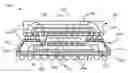
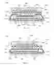
Referring now to FIG. 1, therein is shown a top view of an integrated circuit package system 100 in a first embodiment of the present invention. The integrated circuit package system 100 is shown having a second external device 102 mounted over a redistribution line (RDL) 104.
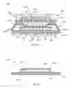
Referring now to FIG. 2, therein is shown a cross-sectional view of the integrated circuit package system 100 along the line 2-2 of FIG. 1. The integrated circuit package system 100 is shown having a substrate 202 such as a laminated plastic or ceramic substrate.
Mounted below the substrate 202 are interconnects, such as solder balls 204. Mounted above the substrate 202 is an internal device 206 such as an integrated circuit die with a functional side 208. The functional side 208 of the internal device 206 is connected to the substrate 202 with bond wires 210.
The internal device 206 is attached to the substrate 202 with a die attach adhesive 212. Partially encapsulating the internal device 206 is an encapsulation 218. The encapsulation 218, such as an epoxy mold compound, has mold risers 220.
The encapsulation 218 has an outer surface 222. Attached to the outer surface 222 is the redistribution line (RDL) 104. The RDL 104 conducts electrical signals, routing them between connection points 226.
The RDL 104 covers the outer surface 222 of the encapsulation 218 and a portion of the functional side 208 of the internal device 206. The RDL 104 may also have an insulator such as a solder mask 228 between connection points 226. The solder mask 228 may be a liquid photoimageable solder mask (LPSM) or dry film photoimageable solder mask (DFSM).
The solder mask 228 prevents solder from bridging between the connection points 226 and the RDL 104, thereby preventing short circuits. Mounted above the internal device 206 and the RDL 104 is a first external device 230 such as a wafer level chip scale package (WLCSP), a redistributed line (RDL) die, or an area array package.
The first external package 230 is connected to the RDL 104 with the solder balls 204. Between the solder balls 204 is an under-fill 232. The under-fill 232 helps to stabilize the first external device 230 and to secure the solder balls 204.
Mounted above the first external device 230 is the second external device 102. The second external device 102 is connected to the mold risers 220 with the solder balls 204. The mold risers 220 provide a standoff height 236, which allows the second external device 102 to have a finer pitch.
The second external device 102 is shown having two wire-bonded die 238 connected to an external device substrate 240 with the bond wires 210. The two wire-bonded die 238 are attached with the die attach adhesive 212.
The RDL 104 electrically connects the substrate 202 to the second external device 102, the first external device 230 and the internal device 206.
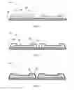
Referring now to FIG. 3, therein is shown the integrated circuit package system 100 of FIG. 2 in an encapsulation phase of manufacture. The integrated circuit package system 100 is shown having the internal device 206 partially encapsulated and partially exposed by the encapsulation 218.
The internal device 206 is shown having the functional side 208 connected to the substrate 202 with the bond wires 210. An exposed surface 302 of the internal device 206 is shown exposed from the encapsulation 218.
Referring now to FIG. 4, therein is shown the integrated circuit package system 100 of FIG. 2 in a thin-metal phase of manufacture. The integrated circuit package system 100 is shown having a seed layer 402 plated to the outer surface 222 of the encapsulation 218 and to the functional side 208 of the internal device 206. The seed layer 402 may be 2 μm to 5 μm.
Referring now to FIG. 5, therein is shown the integrated circuit package system 100 of FIG. 2 in thick-metal phase of manufacture. The integrated circuit package system 100 is shown having a thick metal layer 502 plated on the seed layer 402. The thick metal layer 502 is thicker than the seed layer 402 and may be 12 μm.
Referring now to FIG. 6, therein is shown the integrated circuit package system 100 of FIG. 2 in an etch phase of manufacture. The integrated circuit package system 100 is shown having a pattern 602 etched through the seed layer 402 and the thick metal layer 502. The connection points 226 are visible in this phase of manufacture.
Referring now to FIG. 7, therein is shown the integrated circuit package system 100 of FIG. 2 in a solder mask phase of manufacture. The integrated circuit package system 100 is shown having the solder mask 228 deposited between the connection points 226.
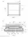
Referring now to FIG. 8, therein is shown a cross-sectional view of an integrated circuit package system 800 in a second embodiment of the present invention. The integrated circuit package system 800 is shown having a substrate 802 such as a laminated plastic or ceramic substrate.
Mounted below the substrate 802 are interconnects, such as solder balls 804. Mounted above the substrate 802 is an internal device 806 such as an integrated circuit die with a functional side 808 and internal device bond-pads 810.
The internal device 806 is attached to the substrate 802 with a die attach adhesive 812. Partially encapsulating the internal device 806 is an encapsulation 818. The encapsulation 818, such as an epoxy mold compound, has mold risers 820.
The encapsulation 818 has an outer surface 822. Attached to the outer surface 822 is a redistribution line (RDL) 824. The RDL 824 conducts electrical signals, routing them between connection points 826.
The RDL 824 covers the outer surface 822 of the encapsulation 818 and a portion of the functional side 808 of the internal device 806. The RDL 824 may also have a solder mask 828 such as a liquid photoimageable solder mask (LPSM) or dry film photoimageable solder mask (DFSM).
The solder mask 828 prevents solder from bridging between the connection points 826 on the RDL 824, thereby preventing short circuits. Mounted above the internal device 806 and the RDL 824 is a first external device 830 such as a wafer level chip scale package (WLCSP), a redistributed line (RDL) die, or an area array package.
The first external package 830 is connected to the RDL 824 with the solder balls 804. Between the solder balls 804 is an under-fill 832. The under-fill 832 helps to stabilize the first external device 830 and to secure the solder balls 804.
Mounted above the first external device 830 is a second external device 834. The second external device 834 is connected to the mold risers 820 with the solder balls 804. The mold risers 820 provide a standoff height 836, which allows the second external device 834 to have a finer pitch.
The second external device 834 is shown having two wire-bonded die 838 connected to an external device substrate 840 with bond wires 842. The two wire-bonded die 838 are attached with the die attach adhesive 812.
The RDL 824 electrically connects the substrate 802 to the second external device 834, the first external device 830 and the internal device 806.
Referring now to FIG. 9, therein is shown the integrated circuit package system 800 of FIG. 8 in a device-mounting phase of manufacture. The integrated circuit package system 800 is shown having the RDL 824 attached to the functional side 808 of the internal device 806.
The RDL 824 electrically connects the internal device bond-pads 810. The internal device 806 is attached to the substrate 802 with the die attach adhesive 812. Importantly, the RDL 824 is already on the internal device 806 prior to an encapsulation phase.
Referring now to FIG. 10, therein is shown a cross-sectional view of an integrated circuit package system 1000 in a third embodiment of the present invention. The integrated circuit package system 1000 is shown having a substrate 1002 such as a laminated plastic or ceramic substrate.
Mounted below the substrate 1002 are interconnects, such as solder balls 1004. Mounted above the substrate 1002 is an internal device 1006 such as a wire-bonded die with a functional side 1008 and internal device bond-pads 1010.
The internal device 1006 is attached to the substrate 1002 with a die attach adhesive 1012. The functional side 1008 of the internal device 1006 is connected to the substrate 1002 with bond wires 1014.
Fully encapsulating the internal device 1006 is an encapsulation 1018. The encapsulation 1018, such as an epoxy mold compound, has mold risers 1020. The encapsulation 1018 has an outer surface 1022. Attached to the outer surface 1022 is a redistribution line (RDL) 1024. The RDL 1024 conducts electrical signals, routing them between connection points 1026.
The RDL 1024 covers the outer surface 1022 of the encapsulation 1018 and does not contact the functional side 1008 of the internal device 1006. The RDL 1024 may also have a solder mask 1028 such as a liquid photoimageable solder mask (LPSM) or dry film photoimageable solder mask (DFSM).
The solder mask 1028 prevents solder from bridging between the connection points 1026 on the RDL 1024, thereby preventing short circuits. Mounted above the internal device 1006 and the RDL 1024 is a first external device 1030 such as a wafer level chip scale package (WLCSP), a redistributed line (RDL) die, or an area array package.
The first external package 1030 is connected to the RDL 1024 with the solder balls 1004. Between the solder balls 1004 is an under-fill 1032. The under-fill 1032 helps to stabilize the first external device 1030 and to secure the solder balls 1004.
Mounted above the first external device 1030 is a second external device 1034. The second external device 1034 is connected to the mold risers 1020 with the solder balls 1004. The mold risers 1020 provide a standoff height 1036, which allows the second external device 1034 to have a finer pitch.
The second external device 1034 is shown having two wire-bonded die 1038 connected to an external device substrate 1040 with the bond wires 1014. The two wire-bonded die 1038 are attached with the die attach adhesive 1012.
The RDL 1024 electrically connects the substrate 1002 to the second external device 1034, and the first external device 1030.
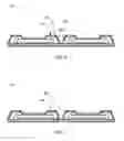
Referring now to FIG. 11, therein is shown a cross-sectional view of an integrated circuit package system 1100 in a fourth embodiment of the present invention. The integrated circuit package system 1100 is shown having a substrate 1102 such as a laminated plastic or ceramic substrate.
Mounted below the substrate 1102 are interconnects, such as solder balls 1104. Mounted above the substrate 1102 is an internal device 1106 such as a flip chip. The internal device 1106 is connected to the substrate 1102 the solder balls 1104. Between the solder balls 1104 is an under fill 1108.
Fully encapsulating the internal device 1106 is an encapsulation 1118. The encapsulation 1118, such as an epoxy mold compound. The encapsulation 1118 has an outer surface 1122. Attached to the outer surface 1122 is a redistribution line (RDL) 1124. The RDL 1124 conducts electrical signals, routing them between connection points 1126.
The RDL 1124 covers the outer surface 1122 of the encapsulation 1118 and does not contact the internal device 1106. The RDL 1124 may also have a solder mask 1128 such as a liquid photoimageable solder mask (LPSM) or dry film photoimageable solder mask (DFSM).
The solder mask 1128 prevents solder from bridging between the connection points 1126 on the RDL 1124, thereby preventing short circuits. Mounted above the internal device 1106 and the RDL 1124 is a first external device 1130 such as a wafer level chip scale package (WLCSP), a redistributed line (RDL) die, or an area array package.
The first external package 1130 is connected to the RDL 1124 with the solder balls 1104. Between the solder balls 1104 is the under-fill 1108. The under-fill 1108 helps to stabilize the first external device 1130 and to secure the solder balls 1104.
Mounted above the first external device 1130 is a second external device 1134. The second external device 1134 is connected to the RDL 1124 with the solder balls 1104. The second external device 1134 is shown having two wire-bonded die 1138 connected to an external device substrate 1140 with bond wires 1142.
The two wire-bonded die 1138 are attached with a die attach adhesive 1144. The RDL 1124 electrically connects the substrate 1102 to the second external device 1134, and the first external device 1130.
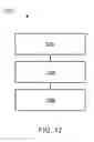
Referring now to FIG. 12, therein is shown a flow chart of a system 1200 for manufacturing the integrated circuit package system 100 of FIG. 1 in an embodiment of the present invention. The system 1200 includes providing an internal device in a block 1202; encapsulating the internal device with an encapsulation having an outer surface in a block 1204; and forming a redistribution line having connection points on the outer surface of the encapsulation in a block 1206.
Thus, it has been discovered that the redistribution on encapsulation of the present invention furnishes important and heretofore unknown and unavailable solutions, capabilities, and functional aspects for package on package configurations. The resulting processes and configurations are straightforward, cost-effective, uncomplicated, highly versatile, accurate, sensitive, and effective, and can be implemented by adapting known components for ready, efficient, and economical manufacturing, application, and utilization.
While the invention has been described in conjunction with a specific best mode, it is to be understood that many alternatives, modifications, and variations will be apparent to those skilled in the art in light of the aforegoing description. Accordingly, it is intended to embrace all such alternatives, modifications, and variations that fall within the scope of the included claims. All matters hithertofore set forth herein or shown in the accompanying drawings are to be interpreted in an illustrative and non-limiting sense.
Claims
What is claimed is:1. An integrated circuit package system comprising:
providing an internal device;
encapsulating the internal device with an encapsulation having an outer surface; and
forming a redistribution line having connection points on the outer surface of the encapsulation.
2. The system as claimed in claim 1 further comprising:
depositing an insulator between the connection points on the redistribution line.
3. The system as claimed in claim 1 wherein:
encapsulating the internal device with the encapsulation includes encapsulating with an encapsulation having mold risers providing a standoff height.
4. The system as claimed in claim 1 further comprising:
forming the redistribution line on an exposed surface of the internal device.
5. The system as claimed in claim 1 wherein:
providing the internal device includes providing an internal device having internal device bond-pads; and
further comprising:
forming the redistribution line on a functional side of the internal device extending to and contacting the internal device bond-pads.
6. An integrated circuit package system comprising:
providing an internal device;
encapsulating the internal device with an encapsulation having an outer surface;
forming a redistribution line having connection points on the outer surface of the encapsulation;
mounting a first external device above the redistribution line and above the internal device; and
connecting the first external device to the redistribution line with an interconnect.
7. The system as claimed in claim 6 further comprising:
mounting a second external device over the redistribution line and over the first external device.
8. The system as claimed in claim 6 wherein:
encapsulating the internal device includes fully encapsulating the internal device with the encapsulation; and
forming the redistribution line includes forming the redistribution line on the encapsulation above the internal device.
9. The system as claimed in claim 6 wherein:
providing the internal device includes providing a flip chip or a wire-bonded die.
10. The system as claimed in claim 6 further comprising:
mounting an under-fill between the first external device and the redistribution line.
11. An integrated circuit package system comprising:
an internal device;
an encapsulation having an outer surface encapsulating the internal device; and
a redistribution line with connection points formed on the outer surface of the encapsulation.
12. The system as claimed in claim 11 further comprising:
an insulator deposited between the connection points on the redistribution line.
13. The system as claimed in claim 11 wherein:
the encapsulation has mold risers providing a standoff height.
14. The system as claimed in claim 11 further comprising:
an exposed surface of the internal device and having the redistribution line formed thereover.
15. The system as claimed in claim 11 further comprising:
an internal device bond-pad on the internal device; and
a functional side of the internal device and having the redistribution line formed thereover and extending to the internal device bond-pad.
16. The system as claimed in claim 11 further comprising:
a first external device mounted above the redistribution line and above the internal device; and
an interconnect connecting the first external device to the redistribution line.
17. The system as claimed in claim 16 further comprising:
a second external device mounted over the redistribution line and over the first external device.
18. The system as claimed in claim 16 wherein:
the internal device is fully encapsulated by the encapsulation; and
the redistribution line is on the encapsulation above the internal device.
19. The system as claimed in claim 16 wherein:
the internal device is a flip chip or a wire-bonded die.
20. The system as claimed in claim 16 further comprising:
an under-fill mounted between the first external device and the redistribution line.
Images & Drawings included:
Sources:
- United States Patent and Trademark Office - verify current appl. status at the USPTO↗
Recent applications in this class:
- » 20250273526 2025-08-28
FULLY MOLDED STRUCTURE WITH MULTI-HEIGHT COMPONENTS COMPRISING BACKSIDE CONDUCTIVE MATERIAL AND METHOD FOR MAKING THE SAME - » 20250266313 2025-08-21
SEMICONDUCTOR DEVICE PACKAGE AND METHOD OF MANUFACTURING THE SAME - » 20250233035 2025-07-17
SEMICONDUCTOR DEVICE AND METHOD OF MANUFACTURING A SEMICONDUCTOR DEVICE - » 20250210432 2025-06-26
ELECTRONIC PACKAGE AND MANUFACTURING METHOD THEREOF - » 20250201645 2025-06-19
FABRICATING PACKAGES WITH DUMMY DIES HAVING A CONSTRUCTION THAT MIMICS WARPAGE OF THE OTHER COMPONENTS INCLUDED IN THE PACKAGE - » 20250191990 2025-06-12
MANUFACTURING METHOD OF SEMICONDUCTOR PACKAGE - » 20250191989 2025-06-12
PACKAGE COMPRISING A SUBSTRATE WITH CAVITY AND AN INTEGRATED DEVICE WITH A STEP BACK SIDE - » 20250157870 2025-05-15
PACKAGE STRUCTURES - » 20250118609 2025-04-10
Semiconductor Packages and Methods of Forming - » 20250079248 2025-03-06
SEMICONDUCTOR PACKAGE AND METHOD OF MANUFACTURING SEMICONDUCTOR PACKAGE
Recent applications for this Assignee:
- » 20160351486 2016-12-01
Semiconductor device and method of forming substrate including embedded component with symmetrical structure - » 20160300817 2016-10-13
Semiconductor device and method of forming a package in-fan out package - » 20160300797 2016-10-13
Double-sided semiconductor package and dual-mold method of making same - » 20160276307 2016-09-22
Semiconductor device and method of forming PoP semiconductor device with RDL over top package - » 20160276238 2016-09-22
Semiconductor device and method of forming supporting layer over semiconductor die in thin fan-out wafer level chip scale package - » 20160233168 2016-08-11
Semiconductor device and method of forming 3D dual side die embedded build-up semiconductor package - » 20160218089 2016-07-28
Semiconductor device and method of forming WLCSP with semiconductor die embedded within interconnect structure - » 20160214857 2016-07-28
Semiconductor device and method of forming MEMS package - » 20160197059 2016-07-07
Semiconductor device and method of forming shielding layer over integrated passive device using conductive channels - » 20160197022 2016-07-07
Semiconductor device and method of forming sacrificial adhesive over contact pads of semiconductor die