Method of manufacturing a chip embedded printed circuit board
US20100142170A1
2010-06-10
12/320,492
2009-01-27
✅ Patent granted
US 8,893,380 B2
2014-11-25
-
-
Donghai D Nguyen
2032-06-14
Abstract:
The present invention relates to a chip embedded printed circuit board and a manufacturing method thereof and provides a chip embedded printed circuit board including: an insulating layer having vias formed therethrough; a first chip and a second chip embedded in the insulating layer and having pads, which are respectively exposed to upper and lower surfaces of the insulating layer, on one surfaces thereof; an upper pattern formed on the upper surface of the insulating layer to be connected to the pads of the first chip and the vias; and a lower pattern formed on the lower surface of the insulating layer to be connected to the pads of the second chip and the vias. Also, the present invention provides a manufacturing method of a chip embedded printed circuit board.
Inventors:
- Tae Sung JEONG 8 🇰🇷 Hwaseong-si, South Korea
- Hong Won KIM 16 🇰🇷 Suwon-si, South Korea
- Sung Yi 26 🇰🇷 Suwon-si, South Korea
- Hong Won Kim 1 🇰🇷 Suwon-si, Gyeonggi-do, South Korea
- Tae Sung Jeong 1 🇰🇷 Hwaseong-si, Gyeonggi-do, South Korea
- Joon Seok Kang 1 🇰🇷 Suwon-si, Gyeonggi-do, South Korea
- Joon Seok Kang 1 🇯🇵 Suwon-si, Japan
Assignee:
- SAMSUNG ELECTRO-MECHANICS CO., LTD. 3,010 🇰🇷 Suwon, South Korea
Applicant:
Interested in similar patents?
Get notified when new applications in this technology area are published.
Classification:
H01L24/19 » CPC further
Arrangements for connecting or disconnecting semiconductor or solid-state bodies; Methods or apparatus related thereto; Means for bonding being attached to, or being formed on, the surface to be connected, e.g. chip-to-package, die-attach, "first-level" interconnects; Manufacturing methods related thereto; High density interconnect [HDI] connectors; Manufacturing methods related thereto Manufacturing methods of high density interconnect preforms
H01L21/568 » CPC further
Processes or apparatus adapted for the manufacture or treatment of semiconductor or solid state devices or of parts thereof; Manufacture or treatment of semiconductor devices or of parts thereof the devices having at least one potential-jump barrier or surface barrier, e.g. PN junction, depletion layer or carrier concentration layer; Assembly of semiconductor devices using processes or apparatus not provided for in a single one of the subgroups - , e.g. sealing of a cap to a base of a container; Encapsulations, e.g. encapsulation layers, coatings Temporary substrate used as encapsulation process aid
H01L2224/04105 » CPC further
Indexing scheme for arrangements for connecting or disconnecting semiconductor or solid-state bodies and methods related thereto as covered by; Means for bonding being attached to, or being formed on, the surface to be connected, e.g. chip-to-package, die-attach, "first-level" interconnects; Manufacturing methods related thereto; Bonding areas; Manufacturing methods related thereto; Structure, shape, material or disposition of the bonding areas prior to the connecting process Bonding areas formed on an encapsulation of the semiconductor or solid-state body, e.g. bonding areas on chip-scale packages
Y10T29/4913 » CPC further
Metal working; Method of mechanical manufacture; Electrical device making; Conductor or circuit manufacturing; On flat or curved insulated base, e.g., printed circuit, etc. Assembling to base an electrical component, e.g., capacitor, etc.
Y10T29/49146 » CPC further
Metal working; Method of mechanical manufacture; Electrical device making; Conductor or circuit manufacturing; On flat or curved insulated base, e.g., printed circuit, etc.; Assembling to base an electrical component, e.g., capacitor, etc. with encapsulating, e.g., potting, etc.
Y10T29/49165 » CPC further
Metal working; Method of mechanical manufacture; Electrical device making; Conductor or circuit manufacturing; On flat or curved insulated base, e.g., printed circuit, etc.; Manufacturing circuit on or in base by forming conductive walled aperture in base
H05K1/185 » CPC main
Printed circuits; Printed circuits structurally associated with non-printed electric components associated with components mounted in the printed circuit board, e.g. insert mounted components [IMC] Components encapsulated in the insulating substrate of the printed circuit or incorporated in internal layers of a multilayer circuit
H01L24/96 » CPC further
Arrangements for connecting or disconnecting semiconductor or solid-state bodies; Methods or apparatus related thereto; Batch processes at chip-level, i.e. with connecting carried out on a plurality of singulated devices, i.e. on diced chips the devices being encapsulated in a common layer, e.g. neo-wafer or pseudo-wafer, said common layer being separable into individual assemblies after connecting
H01L2924/01078 » CPC further
Indexing scheme for arrangements or methods for connecting or disconnecting semiconductor or solid-state bodies as covered by; Chemical elements Platinum [Pt]
H05K2201/10674 » CPC further
Indexing scheme relating to printed circuits covered by; Details of components or other objects attached to or integrated in a printed circuit board; Details of electrical connections of non-printed components, e.g. special leads; Components characterised by their electrical contacts Flip chip
H05K2201/10515 » CPC further
Indexing scheme relating to printed circuits covered by; Details of components or other objects attached to or integrated in a printed circuit board; Details of mounted components; Involving several components Stacked components
H05K2201/10515 » CPC further
Indexing scheme relating to printed circuits covered by; Details of components or other objects attached to or integrated in a printed circuit board; Details of mounted components; Involving several components Stacked components
H01L2924/01029 » CPC further
Indexing scheme for arrangements or methods for connecting or disconnecting semiconductor or solid-state bodies as covered by; Chemical elements Copper [Cu]
H01L24/18 » CPC further
Arrangements for connecting or disconnecting semiconductor or solid-state bodies; Methods or apparatus related thereto; Means for bonding being attached to, or being formed on, the surface to be connected, e.g. chip-to-package, die-attach, "first-level" interconnects; Manufacturing methods related thereto High density interconnect [HDI] connectors; Manufacturing methods related thereto
H01L24/82 » CPC further
Arrangements for connecting or disconnecting semiconductor or solid-state bodies; Methods or apparatus related thereto; Methods for connecting semiconductor or other solid state bodies using means for bonding being attached to, or being formed on, the surface to be connected by forming build-up interconnects at chip-level, e.g. for high density interconnects [HDI]
H01L2924/01059 » CPC further
Indexing scheme for arrangements or methods for connecting or disconnecting semiconductor or solid-state bodies as covered by; Chemical elements Praseodymium [Pr]
H05K3/426 » CPC further
Apparatus or processes for manufacturing printed circuits; Forming printed elements for providing electric connections to or between printed circuits; Plated through-holes or plated via connections characterised by the sequence of steps for plating the through-holes or via connections in relation to the conductive pattern initial plating of through-holes in substrates without metal
H01L2224/18 » CPC further
Indexing scheme for arrangements for connecting or disconnecting semiconductor or solid-state bodies and methods related thereto as covered by; Means for bonding being attached to, or being formed on, the surface to be connected, e.g. chip-to-package, die-attach, "first-level" interconnects; Manufacturing methods related thereto High density interconnect [HDI] connectors; Manufacturing methods related thereto
H01L2924/01033 » CPC further
Indexing scheme for arrangements or methods for connecting or disconnecting semiconductor or solid-state bodies as covered by; Chemical elements Arsenic [As]
H01L21/6835 » CPC further
Processes or apparatus adapted for the manufacture or treatment of semiconductor or solid state devices or of parts thereof; Apparatus specially adapted for handling semiconductor or electric solid state devices during manufacture or treatment thereof; Apparatus specially adapted for handling wafers during manufacture or treatment of semiconductor or electric solid state devices or components ; Apparatus not specifically provided for elsewhere for supporting or gripping using temporarily an auxiliary support
H01L2924/01006 » CPC further
Indexing scheme for arrangements or methods for connecting or disconnecting semiconductor or solid-state bodies as covered by; Chemical elements Carbon [C]
H05K2203/1461 » CPC further
Indexing scheme relating to apparatus or processes for manufacturing printed circuits covered by; Related to the order of processing steps Applying or finishing the circuit pattern after another process, e.g. after filling of vias with conductive paste, after making printed resistors
H05K3/30 IPC
Apparatus or processes for manufacturing printed circuits Assembling printed circuits with electric components, e.g. with resistor
H05K3/30 IPC
Apparatus or processes for manufacturing printed circuits Assembling printed circuits with electric components, e.g. with resistor
H01L23/00 IPC
Details of semiconductor or other solid state devices
H05K1/18 IPC
Printed circuits Printed circuits structurally associated with non-printed electric components
H05K1/18 IPC
Printed circuits Printed circuits structurally associated with non-printed electric components
H01L21/683 IPC
Processes or apparatus adapted for the manufacture or treatment of semiconductor or solid state devices or of parts thereof; Apparatus specially adapted for handling semiconductor or electric solid state devices during manufacture or treatment thereof; Apparatus specially adapted for handling wafers during manufacture or treatment of semiconductor or electric solid state devices or components ; Apparatus not specifically provided for elsewhere for supporting or gripping
H05K3/42 IPC
Apparatus or processes for manufacturing printed circuits; Forming printed elements for providing electric connections to or between printed circuits Plated through-holes or plated via connections
H05K3/42 IPC
Apparatus or processes for manufacturing printed circuits; Forming printed elements for providing electric connections to or between printed circuits Plated through-holes or plated via connections
Description
CROSS-REFERENCE TO RELATED APPLICATIONS
This application claims the benefit of Korean Patent Application No. 10-2008-0122914 filed with the Korea Intellectual Property Office on Dec. 5, 2008, the disclosure of which is incorporated herein by reference.
BACKGROUND OF THE INVENTION
1. Field of the Invention
The present invention relates to a chip embedded printed circuit board and a manufacturing method thereof, and more particularly, to a chip embedded printed circuit board and a manufacturing method thereof capable of embedding a dual-chip in an insulating layer by pressing a pair of carrier plates on which the chips are mounted at upper and lower parts of the insulating layer.
2. Description of the Related Art
Recently, electronic components have been developed to achieve high density and high performance in response to demands for high performance and miniaturization of electronic devices. Therefore, a demand for a small printed circuit board capable of mounting electronic components at high density has been gradually increased. In response to this demand, the development of a multilayer circuit board for electrically connecting between wires or between electronic components and wires formed on different layers through via holes has been progressed.
The multilayer circuit board has advantages of reducing the wires connecting between the electronic components and implementing high density wiring. And, the multilayer circuit board also has advantages of increasing a surface area of a printed circuit board and improving electrical characteristics by mounting the electronic components.
Especially, a demand for an embedded printed circuit board in which electronic components are inserted in a substrate has been gradually increased since it can achieve miniaturization, high density, high performance and the like of the substrate by embedding the electronic components in the substrate without mounting the electronic components on a surface of the substrate.
In case of a conventional chip embedded printed circuit board, a chip is positioned after attaching a perforated core substrate to a tape, and then the tape is removed after laminating an insulating layer such as a prepreg layer on an opposite surface of a surface to which the tape is attached. After that, the prepreg layer is also laminated on the surface from which the tape is removed.
Next, a via hole is formed in a part requiring electrical connection by a laser drilling method and the like, and then a copper plating process and the like are performed.
However, as described above, the conventional chip embedded printed circuit board in which the chip is embedded in the perforated core substrate by using the tape has a disadvantage that it is difficult to reduce an entire thickness of the substrate. Also, as described above, in case of forming the via hole by the laser drilling method and the like, since it is difficult to form the via hole in an accurate position due to a position error of the chip or a tolerance of laser drilling and the like, there are problems such as deterioration of yield and reliability due to connection failure and the like.
SUMMARY OF THE INVENTION
The present invention has been proposed in order to solve the above-described problems, and it is, therefore, an object of the present invention to provide a chip embedded printed circuit board and a manufacturing method thereof capable of reducing an entire thickness of a printed circuit board having a dual-chip embedded therein and improving yield and reliability of products by pressing a pair of the carrier plates on which the chips are mounted at upper and lower parts of an insulating layer to embed the dual-chip in the insulating layer.
In accordance with an aspect of the present invention to achieve the object, there is provided a chip embedded printed circuit board including an insulating layer having vias formed therethrough; a first chip and a second chip embedded in the insulating layer and having pads, which are respectively exposed to upper and lower surfaces of the insulating layer, on one surfaces thereof; an upper pattern formed on the upper surface of the insulating layer to be connected to the pads of the first chip and the vias; and a lower pattern formed on the lower surface of the insulating layer to be connected to the pads of the second chip and the vias.
Here, the first chip and the second chip may be arranged in the insulating layer to be separated from each other.
Also, the first chip and the second chip may be vertically arranged in the insulating layer.
Also, the first chip and the second chip may be horizontally arranged in the insulating layer.
Also, the insulating layer may be made of one of prepreg, ABF (Ajinomoto Build-up Film) and resin.
Also, the chip embedded printed circuit board may further include solder resist layers formed on the upper and lower surfaces of the insulating layer to expose portions of the upper pattern and the lower pattern.
And, in accordance with another aspect of the present invention to achieve the object, there is provided a manufacturing method of a chip embedded printed circuit board including the steps of: mounting chips on a pair of carrier plates respectively such that pads provided on one surfaces of the chips are arranged at lower parts of the chips; arranging an insulating layer between the chips by arranging the chips mounted on the pair of carrier plates to face each other; embedding the chips in the insulating layer by pressing the pair of carrier plates to the insulating layer; exposing the pads provided on the chips by separating the pair of carrier plates from the insulating layer; forming vias penetrating the insulating layer; and forming an upper pattern and a lower pattern on upper and lower surfaces of the insulating layer respectively to be connected to the pads of the chips and the vias.
Here, before the step of mounting the chips on the pair of carrier plates respectively such that pads on one surfaces of the chips are arranged at the lower parts of the chips, the method may further include the step of forming adhesion layers on the pair of carrier plates respectively.
Also, the adhesion layers may be made of one of a UV foam tape, a thermal foam tape and PR.
Also, the insulating layer may be made of one of prepreg, ABF and resin.
Also, in the step of arranging the insulating layer between the chips by arranging the chips mounted on the pair of carrier plates to face each other, the insulating layer may be in a temporarily cured state.
Also, in the step of embedding the chips in the insulating layer by pressing the pair of carrier plates to the insulating layer, the chips embedded in the insulating layer may be arranged to be separated from each other.
Also, after the step of forming the upper pattern and the lower pattern on the upper and lower surfaces of the insulating layer respectively to be connected to the pads of the chips and the vias, the method may further include the step of forming solder resist layers on the upper and lower surfaces of the insulating layer respectively to expose portions of the upper pattern and the lower pattern.
BRIEF DESCRIPTION OF THE DRAWINGS
These and/or other aspects and advantages of the present general inventive concept will become apparent and more readily appreciated from the following description of the embodiments, taken in conjunction with the accompanying drawings of which:
FIG. 1 is a cross-sectional view illustrating a structure of a chip embedded printed circuit board in accordance with an embodiment of the present invention;
FIG. 2 is a cross-sectional view illustrating another structure of the chip embedded printed circuit board in accordance with the embodiment of the present invention; and
FIGS. 3 to 11 are process cross-sectional views sequentially illustrating a manufacturing method of a chip embedded printed circuit board in accordance with another embodiment of the present invention.
DETAILED DESCRIPTION OF THE PREFERRED EMBODIMENTS
Reference will now be made in detail to the embodiments of the present general inventive concept, examples of which are illustrated in the accompanying drawings, wherein like reference numerals refer to like elements throughout. The embodiments are described below in order to explain the present general inventive concept by referring to the figures.
A chip embedded printed circuit board in accordance with an embodiment of the present invention will be described in detail with reference to FIGS. 1 and 2.
FIG. 1 is a cross-sectional view illustrating a structure of the chip embedded printed circuit board in accordance with the embodiment of the present invention, and FIG. 2 is a cross-sectional view illustrating another structure of the chip embedded printed circuit board in accordance with the embodiment of the present invention.
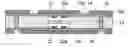
As shown in FIG. 1, the chip embedded printed circuit board in accordance with the embodiment of the present invention includes an insulating layer 13 having vias 15a formed therethrough, a first chip 12 embedded in the insulating layer 13 and having pads 12a, which are exposed to an upper surface of the insulating layer 13, on one surface thereof, a second chip 22 embedded in the insulating layer 13 and having pads 22a, which are exposed to a lower surface of the insulating layer 13, on one surface thereof, an upper pattern 15b formed on the upper surface of the insulating layer 13 to be connected to the pads 12a of the first chip 12 and the vias 15a, and a lower pattern 15c formed on the lower surface of the insulating layer 13 to be connected to the pads 22a of the second chip 22 and the vias 15a.
Here, the first chip 12 and the second chip 22 are arranged in the insulating layer 13 to be separated from each other. At this time, as shown in FIG. 1, the first chip 12 and the second chip 22 may be vertically arranged in the insulating layer 13.
Also, as shown in FIG. 2, the first chip 12 and the second chip 22 may be horizontally arranged in the insulating layer 13, instead of being vertically arranged in the insulating layer 13 as described above.
As shown in FIG. 2, in case that the first and second chips 12 and 22 are horizontally arranged in the insulating layer 13, there is an advantage of reducing an entire thickness of the chip embedded printed circuit board as compared with a case that the first and second chips 12 and 22 are vertically arranged in the insulating layer 13.
The insulating layer 13 having the first and second chips 12 and 22, that is, a dual-chip embedded therein may be made of prepreg, ABF (Ajinomoto Build-up Film), or resin.
And, the vias 15a formed through the insulating layer 13 may be formed by filling insides of via holes 14 with conductive material such as copper through plating and the like after forming the via holes 14 penetrating the insulating layer 13.
The upper pattern 15b and the lower pattern 15c may be made of the same conductive material as the vias 15a such as copper.
Solder resist layers 16 are formed on the upper and lower surfaces of the insulating layer 13 having the dual-chip 12 and 22 embedded therein. At this time, portions of the solder resist layers 16 are removed to expose portions of the upper pattern 15b and the lower pattern 15c.
External connection means such as solder balls (not shown) may be formed on the portions of the upper pattern 15b and the lower pattern 15c, which are exposed by removing the solder resist layers 16.
Since the chip embedded printed circuit board in accordance with the embodiment of the present invention has a structure in which the upper pattern 15b and the lower pattern 15c, which are directly connected to the chips 12 and 22, are formed on the upper and lower surfaces of the insulating layer 13 having the dual-chip 12 and 22 embedded therein, the chip embedded printed circuit board having a two-layered structure in which the total number of layers on which the patterns 15b and 15c are arranged is two can be implemented.
Therefore, in accordance with the embodiment of the present invention, there is an effect of implementing the light, thin and small dual-chip embedded printed circuit board by remarkably reducing the entire thickness of the dual-chip embedded printed circuit board.
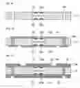
Hereinafter, a manufacturing method of a chip embedded printed circuit board in accordance with another embodiment of the present invention will be described in detail with reference to FIGS. 3 to 11.
FIGS. 3 to 11 are process cross-sectional views sequentially illustrating the manufacturing method of the chip embedded printed circuit board in accordance with the embodiment of the present invention.
First, as shown in FIG. 3, a carrier plate 10 is prepared. At this time, although only one carrier plate 10 is shown in the drawing, it is preferable to prepare a pair of carrier plates 10.
Next, as shown in FIG. 4, adhesion layers 11 are formed on the pair of carrier plates 10, respectively. The adhesion layers 11 may be made of a UV foam tape, a thermal foam tape, or PR.
Then, as shown in FIG. 5, chips 12 are mounted on the pair of carrier plates 10 on which the adhesion layers 11 are formed, respectively. At this time, pads 12a are provided on one surface of each of the chips 12. In the embodiment of the present invention, it is preferable that the chips 12 are mounted on the pair of carrier plates 10 such that the pads 12a provided on the chips 12 are arranged at lower parts of the chips 12.
Next, as shown in FIG. 6, the chips 12 and 22 mounted on the pair of carrier plates 10 are arranged to face each other, and then an insulating layer 13 is arranged between the chips 12 and 22.
The insulating layer 13 may be formed of prepreg, ABF, or resin. Also, it is preferable that the insulating layer 13 is in a temporarily cured state to easily embed the chips 12 and 22 therein in the following process of pressing the pair of carrier plates 10 to embed the dual-chip 12 and 22.
After that, as shown in FIG. 7, the chips 12 and 22 are embedded in the insulating layer 13 by pressing the pair of carrier plates 10 to the insulating layer 13 using compression devices 100 and the like.
At this time, when pressing the pair of carrier plates 10, it is preferable that the chips 12 and 22 embedded in the insulating layer 13 are arranged to be separated from each other without being in contact with each other.
Next, as shown in FIG. 8, the pads 12a and 22a provided on the chips 12 and 22 are exposed by separating the pair of carrier plates 10 from the insulating layer 13 through removal of the adhesion layers 11.
Then, as shown in FIG. 9, via holes 14 penetrating portions of the insulating layer 13 are formed. The via holes 14 are formed by a method such as CNC (Computer Numerical Control) drilling or laser drilling.
Then, as shown in FIG. 10, after vias 15a are formed by filling insides of the via holes 14 with conductive material such as copper, an upper pattern 15b is formed on an upper surface of the insulating layer 13 to be connected to the pads 12a of the chip 12, which is exposed to the upper surface of the insulating layer 13, and the vias 15a, and a lower pattern 15c is formed on a lower surface of the insulating layer 13 to be connected to the pads 22a of the chip 22, which is exposed to the lower surface of the insulating layer 13, and the vias 15a.
Here, the vias 15a, the upper pattern 15b and the lower pattern 15c can be implemented at high density by an SAP (Semi Additive Process) plating method and the like.
Then, as shown in FIG. 11, after solder resist layers 16 are formed on the upper and lower surfaces of the insulating layer 13, portions of the upper pattern 15b and the lower pattern 15c are exposed by removing portions of the solder resist layers 16.
As described above, in accordance with the embodiment of the present invention, since the upper pattern 15b and the lower pattern 15c, which are directly connected to the chips 12 and 22, are formed on the upper and lower surfaces of the insulating layer 13 after embedding the dual-chip 12 and 22 in the insulating layer 13 by pressing the pair of carrier plates on which the chips 12 and 22 are mounted at upper and lower parts of the insulating layer 13 and then separating the pair of carrier plates 10, there is an effect of implementing the light, thin and small dual-chip embedded printed circuit board by remarkably reducing an entire thickness of the printed circuit board having the dual-chip 12 and 22 embedded therein.
Also, in the embodiment of the present invention, since there is no necessity of additionally using a core layer for embedding the chips, and a process of forming vias for connection between the chips and patterns on different layers can be omitted, there are advantages of simplifying processes, reducing manufacturing cost and improving production yield and reliability of the dual-chip embedded printed circuit board.
Although a few embodiments of the present general inventive concept have been shown and described, it will be appreciated by those skilled in the art that changes may be made in these embodiments without departing from the principles and spirit of the general inventive concept, the scope of which is defined in the appended claims and their equivalents.
Claims
1. A chip embedded printed circuit board comprising:
an insulating layer having vias formed therethrough;
a first chip and a second chip embedded in the insulating layer and having pads, which are respectively exposed to an upper surface and a lower surface of the insulating layer, on one surfaces thereof;
an upper pattern formed on the upper surface of the insulating layer to be connected to the pads of the first chip and the vias; and
a lower pattern formed on the lower surface of the insulating layer to be connected to the pads of the second chip and the vias.
2. The chip embedded printed circuit board according to claim 1, wherein the first chip and the second chip are arranged in the insulating layer to be separated from each other.
3. The chip embedded printed circuit board according to claim 2, wherein the first chip and the second chip are vertically arranged in the insulating layer.
4. The chip embedded printed circuit board according to claim 2, wherein the first chip and the second chip are horizontally arranged in the insulating layer.
5. The chip embedded printed circuit board according to claim 1, wherein the insulating layer is made of one of prepreg, ABF (Ajinomoto Build-up Film) and resin.
6. The chip embedded printed circuit board according to claim 1, further comprising solder resist layers formed on the upper and lower surfaces of the insulating layer to expose portions of the upper pattern and the lower pattern.
7. A manufacturing method of a chip embedded printed circuit board comprising:
mounting chips on a pair of carrier plates respectively such that pads on one surfaces of the chips are arranged at lower parts of the chips;
arranging an insulating layer between the chips by arranging the chips mounted on the pair of carrier plates to face each other;
embedding the chips in the insulating layer by pressing the pair of carrier plates to the insulating layer;
exposing the pads provided on the chips by separating the pair of carrier plates from the insulating layer;
forming vias penetrating the insulating layer; and
forming an upper pattern and a lower pattern on upper and lower surfaces of the insulating layer respectively to be connected to the pads of the chips and the vias.
8. The method according to claim 7, further comprising forming adhesion layers on the pair of carrier plates respectively, before the mounting the chips on the pair of carrier plates such that the pads provided on one surfaces of the chips are arranged at the lower parts of the chips.
9. The method according to claim 8, wherein the adhesion layers are made of one of a UV foam tape, a thermal foam tape and PR.
10. The method according to claim 7, wherein the insulating layer is made of one of prepreg, ABF and resin.
11. The method according to claim 7, wherein in the arranging the insulating layer between the chips by arranging the chips mounted on the pair of carrier plates to face each other, the insulating layer is in a temporarily cured state.
12. The method according to claim 7, wherein in the embedding the chips in the insulating layer by pressing the pair of carrier plates to the insulating layer, the chips embedded in the insulating layer are arranged to be separated from each other.
13. The method according to claim 7, after the forming the upper pattern and the lower pattern on the upper and lower surfaces of the insulating layer respectively to be connected to the pads of the chips and the vias, further comprising forming solder resist layers on the upper and lower surfaces of the insulating layer respectively to expose portions of the upper pattern and the lower pattern.
Images & Drawings included:

Sources:
- United States Patent and Trademark Office - verify current appl. status at the USPTO↗
Similar patent applications:
- » 20090321118
Printed circuit board embedded chip and manufacturing method thereof - » 20070007636
Parallel chip embedded printed circuit board and manufacturing method thereof - » 20080314621
Parallel chip embedded printed circuit board and manufacturing method thereof - » 20120042513
Manufacturing method of printed circuit board embedded chip - » 20100134991
Method of manufacturing a chip embedded printed circuit board - » 20060191711
Embedded chip printed circuit board and method of manufacturing the same - » 20140159222
Chip-embedded printed circuit board and semiconductor package using the PCB, and manufacturing method of the PCB
Recent applications in this class:
- » 20250294684 2025-09-18
PRINTED CIRCUIT BOARD WITH MOLD ADHESION BOUNDARY FOR DIE ATTACH PAD - » 20250267795 2025-08-21
Component Carrier With Constricted Through Hole and Electrically Insulating Coating - » 20250261314 2025-08-14
SUBSTRATE WITH BUILT-IN ELECTRONIC COMPONENTS - » 20250227851 2025-07-10
SUBSTRATE SUPPORT WITH PRINTED HEATER - » 20250220818 2025-07-03
FLOW ENHANCED DUMMY STRUCTURE TO ENABLE CAPILLARY FLOW BASED SIDEWALL FILLING - » 20250212336 2025-06-26
PRINTED CIRCUIT BOARD - » 20250212335 2025-06-26
PRINTED CIRCUIT BOARD - » 20250203782 2025-06-19
ELECTRONIC COMPONENT AND METHOD FOR MANUFACTURING SAME - » 20250203781 2025-06-19
RADIO FREQUENCY MODULE AND METHOD FOR MANUFACTURING THE SAME - » 20250168987 2025-05-22
MOLDED PACKAGES WITH THROUGH-MOLD INTERCONNECTS
Recent applications for this Assignee:
- » 20170293104 2017-10-12
Lens module - » 20160242284 2016-08-18
PRINTED CIRCUIT BOARD HAVING METAL BUMPS - » 20160148750 2016-05-26
COIL COMPONENT - » 20160126745 2016-05-05
Non-contact type power transmitting apparatus, non-contact type power receiving apparatus, and non-contact type power transceiving apparatus - » 20160088201 2016-03-24
CAMERA MODULE - » 20160037624 2016-02-04
FLEXIBLE PRINTED CIRCUIT BOARD AND MANUFACTURING METHOD THEREOF - » 20150373842 2015-12-24
SUBSTRATE STRIP, SUBSTRATE PANEL, AND MANUFACTURING METHOD OF SUBSTRATE STRIP - » 20150364992 2015-12-17
Charge pump system and charge pump protection circuit - » 20150364585 2015-12-17
POWER SEMICONDUCTOR DEVICE - » 20150355777 2015-12-10
Integration circuit, touch interaction sensing apparatus, and touchscreen apparatus