Multilayer wiring substrate having a castellation structure
US20100244166A1
2010-09-30
12/659,258
2010-03-02
✅ Patent granted
US 8,344,501 B2
2013-01-01
-
-
Ida M Soward
2031-01-19
Abstract:
A multilayer wiring substrate has a through hole that passes from a first surface through to a second surface. The multilayer wiring substrate includes an electrical connection terminal formed in at least one of an inner edge portion which is a periphery of the through hole, an outer edge portion which is an outer periphery of the substrate, and a non-edge portion, on at least one of the first surface and the second surface. The electrical connection terminal has a castellation structure that does not pass through to a surface opposite to a formation surface.
Inventors:
- Yukihiko Tsukuda 2 🇯🇵 Aichi, Japan
- Tomoyasu Yamada 3 🇯🇵 Aichi, Japan
- Noriko Shibuta 1 🇯🇵 Aichi, Japan
- Tohru Terasaki 1 🇯🇵 Aichi, Japan
- Nobuo Naito 1 🇯🇵 Aichi, Japan
- Ryu Nonoyama 1 🇯🇵 Aichi, Japan
Assignee:
- Sony Corporation 43,269 🇯🇵 Tokyo, Japan
Applicant:
Interested in similar patents?
Get notified when new applications in this technology area are published.
Classification:
H01L29/267 IPC
Semiconductor devices adapted for rectifying, amplifying, oscillating or switching, or capacitors or resistors with at least one potential-jump barrier or surface barrier, e.g. PN junction depletion layer or carrier concentration layer; Details of semiconductor bodies or of electrodes thereof; Multistep manufacturing processes therefor; Semiconductor bodies ; Multistep manufacturing processes therefor characterised by the materials of which they are formed including, apart from doping materials or other impurities, elements provided for in two or more of the groups , , , , , e.g. alloys in different semiconductor regions, e.g. heterojunctions
H01L23/053 IPC
Details of semiconductor or other solid state devices; Containers; Seals characterised by the shape of the container or parts, e.g. caps, walls the container being a hollow construction and having an insulating or insulated base as a mounting for the semiconductor body
H01L2224/45099 » CPC further
Indexing scheme for arrangements for connecting or disconnecting semiconductor or solid-state bodies and methods related thereto as covered by; Means for bonding being attached to, or being formed on, the surface to be connected, e.g. chip-to-package, die-attach, "first-level" interconnects; Manufacturing methods related thereto; Wire connectors; Manufacturing methods related thereto; Structure, shape, material or disposition of the wire connectors prior to the connecting process of an individual wire connector; Core members of the connector Material
H01L2924/00014 » CPC further
Indexing scheme for arrangements or methods for connecting or disconnecting semiconductor or solid-state bodies as covered by; Technical content checked by a classifier the subject-matter covered by the group, the symbol of which is combined with the symbol of this group, being disclosed without further technical details
H01L27/14618 » CPC main
Devices consisting of a plurality of semiconductor or other solid-state components formed in or on a common substrate including semiconductor components sensitive to infra-red radiation, light, electromagnetic radiation of shorter wavelength or corpuscular radiation and specially adapted either for the conversion of the energy of such radiation into electrical energy or for the control of electrical energy by such radiation; Devices controlled by radiation; Imager structures; Structural or functional details thereof Containers
H01L27/14683 » CPC further
Devices consisting of a plurality of semiconductor or other solid-state components formed in or on a common substrate including semiconductor components sensitive to infra-red radiation, light, electromagnetic radiation of shorter wavelength or corpuscular radiation and specially adapted either for the conversion of the energy of such radiation into electrical energy or for the control of electrical energy by such radiation; Devices controlled by radiation; Imager structures Processes or apparatus peculiar to the manufacture or treatment of these devices or parts thereof
H01L24/16 » CPC further
Arrangements for connecting or disconnecting semiconductor or solid-state bodies; Methods or apparatus related thereto; Means for bonding being attached to, or being formed on, the surface to be connected, e.g. chip-to-package, die-attach, "first-level" interconnects; Manufacturing methods related thereto; Bump connectors ; Manufacturing methods related thereto; Structure, shape, material or disposition of the bump connectors after the connecting process of an individual bump connector
H01L24/31 » CPC further
Arrangements for connecting or disconnecting semiconductor or solid-state bodies; Methods or apparatus related thereto; Means for bonding being attached to, or being formed on, the surface to be connected, e.g. chip-to-package, die-attach, "first-level" interconnects; Manufacturing methods related thereto; Layer connectors, e.g. plate connectors, solder or adhesive layers; Manufacturing methods related thereto Structure, shape, material or disposition of the layer connectors after the connecting process
H01L24/48 » CPC further
Arrangements for connecting or disconnecting semiconductor or solid-state bodies; Methods or apparatus related thereto; Means for bonding being attached to, or being formed on, the surface to be connected, e.g. chip-to-package, die-attach, "first-level" interconnects; Manufacturing methods related thereto; Wire connectors; Manufacturing methods related thereto; Structure, shape, material or disposition of the wire connectors after the connecting process of an individual wire connector
H01L24/73 » CPC further
Arrangements for connecting or disconnecting semiconductor or solid-state bodies; Methods or apparatus related thereto Means for bonding being of different types provided for in two or more of groups , , , , , , ,
H01L27/14621 » CPC further
Devices consisting of a plurality of semiconductor or other solid-state components formed in or on a common substrate including semiconductor components sensitive to infra-red radiation, light, electromagnetic radiation of shorter wavelength or corpuscular radiation and specially adapted either for the conversion of the energy of such radiation into electrical energy or for the control of electrical energy by such radiation; Devices controlled by radiation; Imager structures; Structural or functional details thereof; Coatings Colour filter arrangements
H01L2224/04042 » CPC further
Indexing scheme for arrangements for connecting or disconnecting semiconductor or solid-state bodies and methods related thereto as covered by; Means for bonding being attached to, or being formed on, the surface to be connected, e.g. chip-to-package, die-attach, "first-level" interconnects; Manufacturing methods related thereto; Bonding areas; Manufacturing methods related thereto; Structure, shape, material or disposition of the bonding areas prior to the connecting process Bonding areas specifically adapted for wire connectors, e.g. wirebond pads
H01L2224/16 » CPC further
Indexing scheme for arrangements for connecting or disconnecting semiconductor or solid-state bodies and methods related thereto as covered by; Means for bonding being attached to, or being formed on, the surface to be connected, e.g. chip-to-package, die-attach, "first-level" interconnects; Manufacturing methods related thereto; Bump connectors; Manufacturing methods related thereto; Structure, shape, material or disposition of the bump connectors after the connecting process of an individual bump connector
H01L2924/01078 » CPC further
Indexing scheme for arrangements or methods for connecting or disconnecting semiconductor or solid-state bodies as covered by; Chemical elements Platinum [Pt]
H01L2924/01079 » CPC further
Indexing scheme for arrangements or methods for connecting or disconnecting semiconductor or solid-state bodies as covered by; Chemical elements Gold [Au]
H01L2924/14 » CPC further
Indexing scheme for arrangements or methods for connecting or disconnecting semiconductor or solid-state bodies as covered by; Details of semiconductor or other solid state devices to be connected; Device type Integrated circuits
H01L2924/15151 » CPC further
Indexing scheme for arrangements or methods for connecting or disconnecting semiconductor or solid-state bodies as covered by; Details of package parts other than the semiconductor or other solid state devices to be connected; Die mounting substrate; Shape the die mounting substrate comprising an aperture, e.g. for underfilling, outgassing, window type wire connections
H01L2924/15156 » CPC further
Indexing scheme for arrangements or methods for connecting or disconnecting semiconductor or solid-state bodies as covered by; Details of package parts other than the semiconductor or other solid state devices to be connected; Die mounting substrate; Shape the die mounting substrate comprising a recess for hosting the device the shape of the recess being other than a cuboid Side view
H01L2924/15157 » CPC further
Indexing scheme for arrangements or methods for connecting or disconnecting semiconductor or solid-state bodies as covered by; Details of package parts other than the semiconductor or other solid state devices to be connected; Die mounting substrate; Shape the die mounting substrate comprising a recess for hosting the device the shape of the recess being other than a cuboid Top view
H01L2924/16195 » CPC further
Indexing scheme for arrangements or methods for connecting or disconnecting semiconductor or solid-state bodies as covered by; Details of package parts other than the semiconductor or other solid state devices to be connected; Cap; Shape Flat cap [not enclosing an internal cavity]
H01L2924/19043 » CPC further
Indexing scheme for arrangements or methods for connecting or disconnecting semiconductor or solid-state bodies as covered by; Details of hybrid assemblies other than the semiconductor or other solid state devices to be connected; Structure; Component type being a resistor
H01L2924/19105 » CPC further
Indexing scheme for arrangements or methods for connecting or disconnecting semiconductor or solid-state bodies as covered by; Details of hybrid assemblies other than the semiconductor or other solid state devices to be connected; Disposition of discrete passive components in a side-by-side arrangement on a common die mounting substrate
H01L2924/207 » CPC further
Indexing scheme for arrangements or methods for connecting or disconnecting semiconductor or solid-state bodies as covered by; Parameters Diameter ranges
H01L2924/15311 » CPC further
Indexing scheme for arrangements or methods for connecting or disconnecting semiconductor or solid-state bodies as covered by; Details of package parts other than the semiconductor or other solid state devices to be connected; Die mounting substrate; Connection portion the connection portion being formed only on the surface of the substrate opposite to the die mounting surface being a ball array, e.g. BGA
H01L2224/92247 » CPC further
Indexing scheme for arrangements for connecting or disconnecting semiconductor or solid-state bodies and methods related thereto as covered by; Methods for connecting semiconductor or solid state bodies including different methods provided for in two or more of groups - ; Specific sequence of method steps; Connecting different surfaces of the semiconductor or solid-state body with connectors of different types; Sequential connecting processes the first connecting process involving a layer connector the second connecting process involving a wire connector
H01L2924/00012 » CPC further
Indexing scheme for arrangements or methods for connecting or disconnecting semiconductor or solid-state bodies as covered by; Technical content checked by a classifier Relevant to the scope of the group, the symbol of which is combined with the symbol of this group
H01L2224/73265 » CPC further
Indexing scheme for arrangements for connecting or disconnecting semiconductor or solid-state bodies and methods related thereto as covered by; Means for bonding being of different types provided for in two or more of groups; Location after the connecting process on different surfaces Layer and wire connectors
H01L2924/00 » CPC further
Indexing scheme for arrangements or methods for connecting or disconnecting semiconductor or solid-state bodies as covered by
H01L2924/00011 » CPC further
Indexing scheme for arrangements or methods for connecting or disconnecting semiconductor or solid-state bodies as covered by; Technical content checked by a classifier Not relevant to the scope of the group, the symbol of which is combined with the symbol of this group
H01L2224/0401 » CPC further
Indexing scheme for arrangements for connecting or disconnecting semiconductor or solid-state bodies and methods related thereto as covered by; Means for bonding being attached to, or being formed on, the surface to be connected, e.g. chip-to-package, die-attach, "first-level" interconnects; Manufacturing methods related thereto; Bonding areas; Manufacturing methods related thereto; Structure, shape, material or disposition of the bonding areas prior to the connecting process Bonding areas specifically adapted for bump connectors, e.g. under bump metallisation [UBM]
H01L31/0232 IPC
Semiconductor devices sensitive to infra-red radiation, light, electromagnetic radiation of shorter wavelength or corpuscular radiation and specially adapted either for the conversion of the energy of such radiation into electrical energy or for the control of electrical energy by such radiation; Processes or apparatus specially adapted for the manufacture or treatment thereof or of parts thereof; Details thereof; Details Optical elements or arrangements associated with the device
H05K1/11 IPC
Printed circuits; Details Printed elements for providing electric connections to or between printed circuits
H05K1/11 IPC
Printed circuits; Details Printed elements for providing electric connections to or between printed circuits
H01L31/18 IPC
Semiconductor devices sensitive to infra-red radiation, light, electromagnetic radiation of shorter wavelength or corpuscular radiation and specially adapted either for the conversion of the energy of such radiation into electrical energy or for the control of electrical energy by such radiation; Processes or apparatus specially adapted for the manufacture or treatment thereof or of parts thereof; Details thereof Processes or apparatus specially adapted for the manufacture or treatment of these devices or of parts thereof
H01L31/0203 » CPC further
Semiconductor devices sensitive to infra-red radiation, light, electromagnetic radiation of shorter wavelength or corpuscular radiation and specially adapted either for the conversion of the energy of such radiation into electrical energy or for the control of electrical energy by such radiation; Processes or apparatus specially adapted for the manufacture or treatment thereof or of parts thereof; Details thereof; Details Containers; Encapsulations, e.g. encapsulation of photodiodes
H01L27/15 IPC
Devices consisting of a plurality of semiconductor or other solid-state components formed in or on a common substrate including semiconductor components with at least one potential-jump barrier or surface barrier specially adapted for light emission
H01L31/12 IPC
Semiconductor devices sensitive to infra-red radiation, light, electromagnetic radiation of shorter wavelength or corpuscular radiation and specially adapted either for the conversion of the energy of such radiation into electrical energy or for the control of electrical energy by such radiation; Processes or apparatus specially adapted for the manufacture or treatment thereof or of parts thereof; Details thereof structurally associated with, e.g. formed in or on a common substrate with, one or more electric light sources, e.g. electroluminescent light sources, and electrically or optically coupled thereto
H01L33/00 IPC
Semiconductor devices with at least one potential-jump barrier or surface barrier specially adapted for light emission; Processes or apparatus specially adapted for the manufacture or treatment thereof or of parts thereof; Details thereof
H01L29/73 IPC
Semiconductor devices adapted for rectifying, amplifying, oscillating or switching, or capacitors or resistors with at least one potential-jump barrier or surface barrier, e.g. PN junction depletion layer or carrier concentration layer; Details of semiconductor bodies or of electrodes thereof; Multistep manufacturing processes therefor; Types of semiconductor device ; Multistep manufacturing processes therefor controllable by only the electric current supplied, or only the electric potential applied, to an electrode which does not carry the current to be rectified, amplified or switched; Bipolar devices; Transistor-type devices, i.e. able to continuously respond to applied control signals Bipolar junction transistors
H01L29/74 IPC
Semiconductor devices adapted for rectifying, amplifying, oscillating or switching, or capacitors or resistors with at least one potential-jump barrier or surface barrier, e.g. PN junction depletion layer or carrier concentration layer; Details of semiconductor bodies or of electrodes thereof; Multistep manufacturing processes therefor; Types of semiconductor device ; Multistep manufacturing processes therefor controllable by only the electric current supplied, or only the electric potential applied, to an electrode which does not carry the current to be rectified, amplified or switched; Bipolar devices Thyristor-type devices, e.g. having four-zone regenerative action
H01L23/12 IPC
Details of semiconductor or other solid state devices Mountings, e.g. non-detachable insulating substrates
H01L31/111 IPC
Semiconductor devices sensitive to infra-red radiation, light, electromagnetic radiation of shorter wavelength or corpuscular radiation and specially adapted either for the conversion of the energy of such radiation into electrical energy or for the control of electrical energy by such radiation; Processes or apparatus specially adapted for the manufacture or treatment thereof or of parts thereof; Details thereof in which radiation controls flow of current through the device, e.g. photoresistors characterised by at least one potential-jump barrier or surface barrier, e.g. phototransistors; Devices sensitive to infra-red, visible or ultra-violet radiation characterised by at least three potential barriers, e.g. photothyristor
H01L31/00 IPC
Semiconductor devices sensitive to infra-red radiation, light, electromagnetic radiation of shorter wavelength or corpuscular radiation and specially adapted either for the conversion of the energy of such radiation into electrical energy or for the control of electrical energy by such radiation; Processes or apparatus specially adapted for the manufacture or treatment thereof or of parts thereof; Details thereof
H01L29/40 IPC
Semiconductor devices adapted for rectifying, amplifying, oscillating or switching, or capacitors or resistors with at least one potential-jump barrier or surface barrier, e.g. PN junction depletion layer or carrier concentration layer; Details of semiconductor bodies or of electrodes thereof; Multistep manufacturing processes therefor Electrodes ; Multistep manufacturing processes therefor
Description
BACKGROUND OF THE INVENTION
1. Field of the Invention
The present invention relates to a multilayer wiring substrate, a stack structure sensor package, and a method of manufacturing the stack structure sensor package that are applied to an image sensor and the like.
2. Description of the Related Art
Japanese Unexamined Patent Application Publication No. 2002-353427 proposes a stack structure sensor package of an image sensor.
FIG. 1 illustrates the stack structure sensor package of the image sensor as disclosed in Japanese Unexamined Patent Application Publication No. 2002-353427.
In a sensor package structure in FIG. 1, a frame-shaped second substrate 2 is joined onto a first surface of a first substrate 1, thereby forming a cavity 3.
An integrated circuit 4 is mounted on the first surface of the first substrate 1 in the cavity 3, and an image sensor chip 5 is joined onto the second substrate 2. Thus, the stack structure sensor package is formed.
SUMMARY OF THE INVENTION
However, the above-mentioned structure is limited to a stack-up manufacturing process in which the integrated circuit 4 is joined after the cavity 3 is formed by the first substrate 1 and the second substrate 2. This has the following disadvantages.
Since the stack-up in the same process step is necessary, a manufacturing location is limited.
Besides, occurrence of a failure causes a high disposal cost. In detail, when a failure occurs during manufacture, for example, during image sensor sealing, all components of the stack structure sensor package are disposed of due to the failure.
When the above-mentioned stack structure sensor package is joined to another structure by a junction terminal on a back surface of the first substrate 1, the stack structure sensor package is typically soldered to an organic substrate. However, there may be a problem with connection strength because a joint area is limited to the bottom surface.
Furthermore, since the sensor and the integrated circuit 4 for processing sensor signals are packaged, a component for realizing an additional function is additionally placed outside the package. This contradicts miniaturization.
It is desirable to provide a multilayer wiring substrate, a stack structure sensor package, and a method of manufacturing the stack structure sensor package that enable a sensor component to be reused even when a failure occurs during manufacture, improve connection strength of the sensor component, and make the structure small and thin.
A multilayer wiring substrate according to an embodiment of the present invention has a through hole that passes from a first surface through to a second surface, and includes an electrical connection terminal formed in at least one of an inner edge portion which is a periphery of the through hole, an outer edge portion which is an outer periphery of the substrate, and a non-edge portion, on at least one of the first surface and the second surface. The electrical connection terminal has a castellation structure that does not pass through to a surface opposite to a formation surface.
A stack structure sensor package according to another embodiment of the present invention includes: a multilayer wiring substrate, having a through hole, that includes a wire bonding pad on a first surface and an electrical connection terminal on a second surface, the electrical connection terminal being formed in at least one of an inner edge portion which is a periphery of the through hole, an outer edge portion which is an outer periphery of the substrate, and a non-edge portion; an image sensor that is fixed to the periphery of the through hole on the first surface of the multilayer wiring substrate so as to lay across the through hole of the multilayer wiring substrate, and is electrically connected to the pad by a wire; a frame that is fixed to the outer edge portion on the first surface of the multilayer wiring substrate so as to surround the image sensor; and an optical filter that is fixed to a surface of the frame so as to face the image sensor.
A method of manufacturing a stack structure sensor package according to still another embodiment of the present invention includes the steps of: fixing an image sensor to a periphery of a through hole on a first surface of a multilayer wiring substrate so as to lay across the through hole of the multilayer wiring substrate, the multilayer wiring substrate having the through hole and including a wire bonding pad on the first surface and an electrical connection terminal on a second surface, the electrical connection terminal being formed in at least one of an inner edge portion which is the periphery of the through hole, an outer edge portion which is an outer periphery of the substrate, and a non-edge portion; electrically connecting the pad of the multilayer wiring substrate and the image sensor by a wire; fixing a frame to the outer edge portion on the first surface of the multilayer wiring substrate so as to surround the image sensor; and fixing an optical filter to a surface of the frame so as to face the image sensor.
According to the embodiments of the present invention, it is possible to reuse a sensor component even when a failure occurs during manufacture of a sensor package having a stack structure, to improve connection strength of the sensor component, and to make the structure small and thin.
BRIEF DESCRIPTION OF THE DRAWINGS
FIG. 1 illustrates a stack structure sensor package of an image sensor as disclosed in Japanese Unexamined Patent Application Publication No. 2002-353427;
FIG. 2 illustrates a structure example of a stack structure sensor package to which a multilayer wiring substrate is applied according to an embodiment of the present invention;
FIG. 3 illustrates a first structure example of the multilayer wiring substrate according to the embodiment of the present invention;
FIG. 4 illustrates a second structure example of the multilayer wiring substrate according to the embodiment of the present invention;
FIG. 5 illustrates a third structure example of the multilayer wiring substrate according to the embodiment of the present invention;
FIG. 6 illustrates a fourth structure example of the multilayer wiring substrate according to the embodiment of the present invention;
FIG. 7 illustrates a fifth structure example of the multilayer wiring substrate according to the embodiment of the present invention;
FIG. 8 illustrates a sixth structure example of the multilayer wiring substrate according to the embodiment of the present invention;
FIG. 9 illustrates a seventh structure example of the multilayer wiring substrate according to the embodiment of the present invention;
FIG. 10 shows the number of electrodes and a result of measured solder strength against thermal shock in each of the multilayer wiring substrates in FIGS. 6 and 3, relative to the multilayer wiring substrate in FIG. 9;
FIGS. 11A to 11D illustrate a method of manufacturing the stack structure sensor package in FIG. 2; and
FIG. 12 illustrates a structure example of a stack structure sensor package to which a multilayer wiring substrate is applied according to another embodiment of the present invention.
DESCRIPTION OF THE PREFERRED EMBODIMENTS
The following describes embodiments of the present invention with reference to the drawings in the following order.
1. Embodiment
2. Another embodiment
1. Embodiment
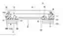
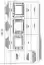
FIG. 2 illustrates a structure example of a stack structure sensor package to which a multilayer wiring substrate is applied according to an embodiment of the present invention.
A sensor package 10 has a stack structure that basically includes a multilayer wiring substrate 11, an image sensor chip 12, a frame 13 formed of ceramic, a resin, or the like, and an optical filter 14 as main components.
The multilayer wiring substrate 11 is a substrate that serves as a base of the stack structure sensor package 10 of an image sensor, and has the following characteristic structure.
A through hole 113 that passes from a first surface (front surface) 111 through to a second surface (back surface) 112 is formed in a center portion of the multilayer wiring substrate 11.
In the multilayer wiring substrate 11, an electrical connection terminal (electrode) is formed in at least one of an inner edge portion IEP which is a periphery of the through hole 113, an outer edge portion OEP which is an outer periphery of the substrate itself, and a non-edge portion, on at least one of the first surface 111 and the second surface 112.
In the multilayer wiring substrate 11, the electrical connection terminal (electrode) formed in at least one of the inner edge portion IEP and the outer edge portion OEP has a castellation (depression) structure that does not pass through to (does not reach) a surface opposite to a formation surface, as described later.
The electrical connection terminal (electrode) formed in at least one of the inner edge portion IEP and the outer edge portion OEP is intended for an improvement in connection strength with another substrate and the like.
Moreover, the castellation structure of the electrical connection terminal (electrode) formed in at least one of the inner edge portion IEP and the outer edge portion OEP has a function of improving the connection strength and also alleviating a stress that acts upon the electrode from the outside and the like.
In the multilayer wiring substrate 11 illustrated in FIG. 2, a wire bonding pad PAD is formed at a center between the inner edge portion IEP and the outer edge portion OEP on the first surface 111, and the electrical connection terminal (electrode) is formed in at least one of the inner edge portion IEP and the outer edge portion OEP on the second surface 112.
In addition, a connection terminal (internal electrode) is formed in a center portion CTP between the inner edge portion IEP and the outer edge portion OEP on the second surface 112 of the multilayer wiring substrate 11.
The following describes more specific structure examples of the multilayer wiring substrate 11, with reference to drawings.
[First Structure Example of the Multilayer Wiring Substrate]
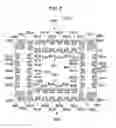
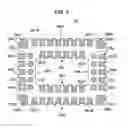
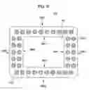
FIG. 3 illustrates a first structure example of the multilayer wiring substrate according to this embodiment.
FIG. 3 illustrates a structure example on the second surface (back surface) 112 side of a multilayer wiring substrate 11A.
The multilayer wiring substrate 11A in FIG. 3 is formed as a rectangular parallelepiped (rectangle) as a whole.
As mentioned earlier, the through hole 113 that passes from the first surface (front surface) 111 through to the second surface (back surface) 112 is formed in the center portion of the multilayer wiring substrate 11A.
In the multilayer wiring substrate 11A in FIG. 3, first electrical connection terminals (referred to below as inner peripheral electrodes) IEL are formed in all of inner edge portions IEP1, IEP2, IEP3, and IEP4 which are the periphery of the through hole 113, on the second surface (back surface) 112.
Moreover, in the multilayer wiring substrate 11A in FIG. 3, second electrical connection terminals (referred to below as outer peripheral electrodes) OEL are formed in all of outer edge portions OEP1, OEP2, OEP3, and OEP4 which are the outer periphery of the substrate itself.
Furthermore, in the multilayer wiring substrate 11A in FIG. 3, electrical connection terminals (referred to below as corner electrodes) OCEL1, OCEL2, OCEL3, and OCEL4 that are included in outer peripheral electrodes are formed respectively in four corners CNR1, CNR2, CNR3, and CNR4 of the outer periphery of the substrate.
In addition, in the multilayer wiring substrate 11A in FIG. 3, third electrical connection terminals (referred to below as internal electrodes) CTEL1, CTEL2, CTEL3, and CTEL4 are formed in non-edge portions (inside) between the inner edge portion IEP1 and the outer edge portion OEP1 and between the inner edge portion IEP3 and the outer edge portion OEP3.
The numbers of inner peripheral electrodes IEL, outer peripheral electrodes OEL, and internal electrodes CTEL illustrated in this embodiment are merely an example. Though the numbers of electrodes are illustrated to be several for the sake of clarity, in actuality the numbers of electrodes are not limited to the illustrated numbers and are appropriately set according to intended use.
In FIG. 3, inner peripheral electrodes IEL11, IEL12, IEL13, IEL14, IEL15, and IEL16 are formed in the inner edge portion IEP1.
The inner peripheral electrodes IEL11, IEL12, IEL13, IEL14, IEL15, and IEL16 are each formed to have a castellation structure in which its side portion facing the through hole 113 is partially depressed in a circular arc.
Inner peripheral electrodes IEL21, IEL22, IEL23, IEL24, and IEL25 are formed in the inner edge portion IEP2.
The inner peripheral electrodes IEL21, IEL22, IEL23, IEL24, and IEL25 are each formed to have a castellation structure in which its side portion facing the through hole 113 is partially depressed in a circular arc.
Inner peripheral electrodes IEL31, IEL32, IEL33, IEL34, IEL35, and IEL36 are formed in the inner edge portion IEP3.
The inner peripheral electrodes IEL31, IEL32, IEL33, IEL34, IEL35, and IEL36 are each formed to have a castellation structure in which its side portion facing the through hole 113 is partially depressed in a circular arc.
Inner peripheral electrodes IEL41, IEL42, IEL43, IEL44, and IEL45 are formed in the inner edge portion IEP4.
The inner peripheral electrodes IEL41, IEL42, IEL43, IEL44, and IEL45 are each formed to have a castellation structure in which its side portion facing the through hole 113 is partially depressed in a circular arc.
In FIG. 3, outer peripheral electrodes OEL11, OEL12, OEL13, OEL14, OEL15, OEL16, OEL17, and OEL18 are formed in the outer edge portion OEP1.
The outer peripheral electrodes OEL11, OEL12, OEL13, OEL14, OEL15, OEL16, OEL17, and OEL18 are each formed to have a castellation structure in which its side portion facing the outside is partially depressed in a circular arc.
Outer peripheral electrodes OEL21, OEL22, OEL23, OEL24, and OEL25 are formed in the outer edge portion OEP2.
The outer peripheral electrodes OEL21, OEL22, OEL23, OEL24, and OEL25 are each formed to have a castellation structure in which its side portion facing the outside is partially depressed in a circular arc.
Outer peripheral electrodes OEL31, OEL32, OEL33, OEL34, OEL35, OEL36, OEL37, and OEL38 are formed in the outer edge portion OEP3.
The outer peripheral electrodes OEL31, OEL32, OEL33, OEL34, OEL35, OEL36, OEL37, and OEL38 are each formed to have a castellation structure in which its side portion facing the outside is partially depressed in a circular arc.
Outer peripheral electrodes OEL41, OEL42, OEL43, OEL44, and OEL45 are formed in the outer edge portion OEP4.
The outer peripheral electrodes OEL41, OEL42, OEL43, OEL44, and OEL45 are each formed to have a castellation structure in which its side portion facing the outside is partially depressed in a circular arc.
Moreover, the corner electrodes OCEL1, OCEL2, OCEL3, and OCEL4 are each formed to have a castellation structure in which its side portion facing the outside is partially depressed in a circular arc.
Thus, in the multilayer wiring substrate 11A in FIG. 3, the inner peripheral electrodes IEL are formed in all of the inner edge portions IEP1, IEP2, IEP3, and IEP4 which are the periphery of the through hole 113, on the second surface (back surface) 112.
Moreover, in the multilayer wiring substrate 11A in FIG. 3, the outer peripheral electrodes OEL are formed in all of the outer edge portions OEP1, OEP2, OEP3, and OEP4 which are the outer periphery of the substrate itself.
Furthermore, in the multilayer wiring substrate 11A in FIG. 3, the corner electrodes OCEL1, OCEL2, OCEL3, and OCEL4 are formed respectively in the four corners CNR1, CNR2, CNR3, and CNR4 of the outer periphery of the substrate.
Since each of these electrodes has a castellation structure, the number of electrodes can be increased and the solder connection strength against thermal shock and the like can be enhanced as compared with, for example, the case where no electrode is provided in any edge portion, as described later.
In addition, the multilayer wiring substrate 11A in FIG. 3 has an effective shape that allows a joint area to be visually inspected when the multilayer wiring substrate 11A is joined to another multilayer wiring substrate, and has an electrode arrangement that takes inspectability into consideration.
[Second Structure Example of the Multilayer Wiring Substrate]
FIG. 4 illustrates a second structure example of the multilayer wiring substrate according to this embodiment.
FIG. 4 illustrates a structure example on the second surface (back surface) 112 side of a multilayer wiring substrate 11B.
The multilayer wiring substrate 11B in FIG. 4 is basically different from the multilayer wiring substrate 11A in FIG. 3 in that the internal electrodes CTEL1, CTEL2, CTEL3, and CTEL4 are not formed.
In the multilayer wiring substrate 11B in FIG. 4, three inner peripheral electrodes IEL21, IEL22, and IEL23 are formed in the inner edge portion IEP2, and three inner peripheral electrodes IEL41, IEL42, and IEL43 are formed in the inner edge portion IEP4.
The multilayer wiring substrate 11B in FIG. 4 also has a shape that allows a joint area to be visually inspected when the multilayer wiring substrate 11B is joined to another multilayer wiring substrate, and has an electrode arrangement that takes inspectability into consideration.
In addition, in the multilayer wiring substrate 11B, the number of electrodes can be increased and the solder connection strength against thermal shock and the like can be enhanced as compared with, for example, the case where no electrode is provided in any edge portion.
[Third Structure Example of the Multilayer Wiring Substrate]
FIG. 5 illustrates a third structure example of the multilayer wiring substrate according to this embodiment.
FIG. 5 illustrates a structure example of the second surface (back surface) 112 side of a multilayer wiring substrate 11C.
The multilayer wiring substrate 11C in FIG. 5 is basically different from the multilayer wiring substrate 11A in FIG. 3 in the following point.
In the multilayer wiring substrate 11C, no inner peripheral electrode is formed in the inner edge portions IEP2 and IEP4, and a plurality of (five in FIG. 5) internal electrodes CTEL are formed in each non-edge portion between the inner edge portion IEP2 and the outer edge portion OEP2 and between the inner edge portion IEP4 and the outer edge portion OEP4.
In the multilayer wiring substrate 11C, the number of electrodes can be increased and the solder connection strength against thermal shock and the like can be enhanced as compared with, for example, the case where no electrode is provided in any edge portion.
[Fourth Structure Example of the Multilayer Wiring Substrate]
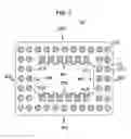
FIG. 6 illustrates a fourth structure example of the multilayer wiring substrate according to this embodiment.
FIG. 6 illustrates a structure example on the second surface (back surface) 112 side of a multilayer wiring substrate 11D.
The multilayer wiring substrate 11D in FIG. 6 is basically different from the multilayer wiring substrate 11C in FIG. 5 in the following point.
In the multilayer wiring substrate 11D, no inner peripheral electrode is formed in any of the inner edge portions IEP1, IEP2, IEP3, and IEP4.
The multilayer wiring substrate 11D has an effective shape for maximizing the through hole 113 to thereby maximize a mounting area inside the through hole 113 when the multilayer wiring substrate 11D is joined to another multilayer wiring substrate.
Moreover, in the multilayer wiring substrate 11D, the number of electrodes can be increased and the solder connection strength against thermal shock and the like can be enhanced as compared with, for example, the case where no electrode is provided in any edge portion.
[Fifth Structure Example of the Multilayer Wiring Substrate]
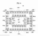
FIG. 7 illustrates a fifth structure example of the multilayer wiring substrate according to this embodiment.
FIG. 7 illustrates a structure example on the second surface (back surface) 112 side of a multilayer wiring substrate 11E.
The multilayer wiring substrate 11E in FIG. 7 is basically different from the multilayer wiring substrate 11C in FIG. 5 in the following point.
In the multilayer wiring substrate 11E, no inner peripheral electrode is formed in the inner edge portions IEP2 and IEP4, no outer peripheral electrode is formed in any of the outer edge portions OEP1 to OEP4, and a plurality of (42 in FIG. 7) internal electrodes CTEL are formed throughout the whole non-edge portion as internal electrodes for connection.
The multilayer wiring substrate 11E has an effective shape for increasing the number of connection terminals and also providing a same mounting area as the outer shape of the multilayer wiring substrate according to this embodiment, when the multilayer wiring substrate 11E is joined to another multilayer wiring substrate.
Moreover, in the multilayer wiring substrate 11E, the number of electrodes can be increased and the solder connection strength against thermal shock and the like can be enhanced as compared with, for example, the case where no electrode is provided in any edge portion.
[Sixth Structure Example of the Multilayer Wiring Substrate]
FIG. 8 illustrates a sixth structure example of the multilayer wiring substrate according to this embodiment.
FIG. 8 illustrates a structure example on the second surface (back surface) 112 side of a multilayer wiring substrate 11F.
The multilayer wiring substrate 11F in FIG. 8 is basically different from the multilayer wiring substrate 11C in FIG. 5 in the following point.
In the multilayer wiring substrate 11F, no outer peripheral electrode is formed in any of the outer edge portions OEP1 to OEP4, and no internal electrode for connection is formed throughout the whole non-edge portion.
In the multilayer wiring substrate 11F, the number of electrodes can be increased and the solder connection strength against thermal shock and the like can be enhanced as compared with, for example, the case where no electrode is provided in any edge portion.
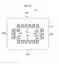
[Seventh Structure Example of the Multilayer Wiring Substrate]
FIG. 9 illustrates a seventh structure example of the multilayer wiring substrate according to this embodiment.
FIG. 9 illustrates a structure example on the second surface (back surface) 112 side of a multilayer wiring substrate 11G.
The multilayer wiring substrate 11G in FIG. 9 is basically different from the multilayer wiring substrate 11D in FIG. 6 in the following point.
In the multilayer wiring substrate 11G, no outer peripheral electrode is formed in any of the outer edge portions OEP1 to OEP4, and a plurality of internal electrodes for connection are formed throughout the whole non-edge portion.
The multilayer wiring substrate 11G has an effective shape for minimizing a mounting area when the multilayer wiring substrate 11G is joined to another multilayer wiring substrate.
In the multilayer wiring substrate 11G, the number of internal electrodes can be increased though the connection strength is lower than the first to sixth structure examples.
The number of electrodes and the solder strength against thermal shock in each of the multilayer wiring substrate 11D in FIG. 6 and the multilayer wiring substrate 11A in FIG. 3 are examined below, relative to the multilayer wiring substrate 11G in FIG. 9.
FIG. 10 shows the number of electrodes and a result of measured solder strength against thermal shock in each of the multilayer wiring substrates in FIGS. 6 and 3, relative to the multilayer wiring substrate in FIG. 9.
In FIG. 10, the connection strength is indicated as a ratio of an actually measured value of a test piece to that of the multilayer wiring substrate 11G in FIG. 9, which is set to 1 as the reference (reference pattern).
In this case, the connection strength of the multilayer wiring substrate 11D in FIG. 6 is 1.71 times that of the multilayer wiring substrate 11G in FIG. 9 as the reference pattern.
The connection strength of the multilayer wiring substrate 11A in FIG. 3 is 1.64 times that of the multilayer wiring substrate 11G in FIG. 9 as the reference pattern.
Meanwhile, when the number of electrodes in the multilayer wiring substrate 11G in FIG. 9 is 40, the number of electrodes in the multilayer wiring substrate 11D in FIG. 6 is 56 which is 1.4 times that of the multilayer wiring substrate 11G in FIG. 9 as the reference pattern.
The number of electrodes in the multilayer wiring substrate 11A in FIG. 3 is 56 which is 1.4 times that of the multilayer wiring substrate 11G in FIG. 9 as the reference pattern.
As described above, in the multilayer wiring substrates 11 and 11A to 11F according to this embodiment, the through hole 113 that passes from the first surface (front surface) 111 through to the second surface (back surface) 112 is formed in the center portion.
In the multilayer wiring substrate 11, an electrical connection terminal (electrode) is formed in at least one of the inner edge portion IEP which is the periphery of the through hole 113, the outer edge portion OEP which is the outer periphery of the substrate itself, and the non-edge portion, on at least one of the first surface 111 and the second surface 112.
In the multilayer wiring substrate 11, the electrical connection terminal (electrode) formed in at least one of the inner, edge portion IEP and the outer edge portion OEP has a castellation (depression) structure that does not pass through to (does not reach) a surface opposite to a formation surface.
Accordingly, the multilayer wiring substrates 11 and 11A to 11F can improve the strength of connection to another substrate and the like and also increase the number of electrodes (the number of terminals).
Moreover, the multilayer wiring substrate 11G can minimize the mounting area when being joined to another multilayer wiring substrate.
The stack structure sensor package 10 in FIG. 2 using any of the multilayer wiring substrates 11 and 11A to 11G having the above-mentioned features allows a sensor component to be reused even when a failure occurs during manufacture, improves connection strength of the sensor component, and makes the structure small and thin.
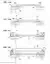
FIGS. 11A to 11D illustrate a method of manufacturing the stack structure sensor package 10 in FIG. 2.
The method of manufacturing the stack structure sensor package 10 in FIG. 2 is described below, with reference to FIGS. 11A to 11D.
First, as illustrated in FIG. 11A, the image sensor 12 is fixed, by an adhesive 15, to the surface of the multilayer wiring substrate 11 that has the through hole 113 and includes the wire bonding pad PAD on the first surface (front surface) 111 and at least any of the electrodes IEL, OEL, and CTEL for connection to another substrate on the second surface (back surface) 112.
Next, as illustrated in FIG. 11B, the image sensor 12 and the pad PAD of the multilayer wiring substrate 11 are electrically connected by a wire 16.
Following this, as illustrated in FIG. 11C, the frame 13 is fixed to the first surface (front surface) 111 of the multilayer wiring substrate 11 by an adhesive 17 so as to surround the image sensor 12.
Subsequently, as illustrated in FIG. 11D, the optical filter 14 is bonded to a surface of the frame 13 formed of ceramic, a resin, or the like by an adhesive 18 and sealed together.
This completes the manufacture of the stack structure sensor package 10 in FIG. 2 as an image sensor component.
The stack structure sensor package 10 in FIG. 2 manufactured in this way allows a sensor component to be reused even when a failure occurs during manufacture, improves connection strength of the sensor component, and makes the structure small and thin.
2. Another Embodiment
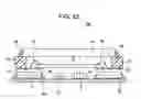
FIG. 12 illustrates a structure example of a stack structure sensor package to which a multilayer wiring substrate is applied according to another embodiment of the present invention.
A stack structure sensor package 10A according to the other embodiment is different from the sensor package 10 according to the embodiment described earlier in the following point.
In the stack structure sensor package 10A, an organic multilayer substrate 20 on which electronic devices such as an integrated circuit 21 and an electronic component 22 like a resistor are mounted is connected to the second surface (back surface) 112 of the multilayer wiring substrate 11 at the above-mentioned connection terminals (electrodes), by solder 24.
The stack structure sensor package 10A is formed through the following manufacturing process after manufacturing the sensor package 10 in FIG. 2 as described earlier.
The integrated circuit 21 and the electronic component 22 are mounted on the organic multilayer substrate 20 other than the multilayer wiring substrate 11, the sensor package 10 is mounted so as to cover the integrated circuit 21 and the electronic component 22, and the sensor package 10 and the organic multilayer substrate 20 are simultaneously soldered to obtain the sensor package 10A having the stack structure.
The stack structure sensor packages 10 and 10A according to the embodiments have been described above.
In the above description, FIGS. 3 to 9 merely illustrate electrode arrangement examples, and the number of electrodes, a pitch between electrodes, and an electrode size are changed according to intended use.
Moreover, the shapes of the multilayer wiring substrate 11 and the through hole 113 are changed according to intended use.
The multilayer wiring substrate 11 may be any of an organic substrate and an inorganic substrate.
Electrode plating in the multilayer wiring substrate 11 may be copper patterning, gold plating, or rustproofing.
Furthermore, the component mounted under the semiconductor device according to the embodiments may be any of an active component and a passive component.
As described above, according to the embodiments, the multilayer wiring substrate 11 having the through hole 113 is used in the sensor component.
As a result, when packaging the sensor component with the electronic component and the integrated circuit necessary for a sensor package operation in a separate process, the electronic component and the integrated circuit can be placed under the sensor component.
Moreover, the following effects can be attained by the method of manufacturing the stack structure sensor package by which the sensor component can be simultaneously soldered together with these components.
By using the multilayer wiring substrate 11 having the through hole 113, connection terminals can be provided not only on the bottom surface of the substrate but also in the outer periphery of the substrate and the periphery of the through hole. In addition, since each terminal has a castellation structure, a fillet can be formed at the time of soldering, which improves the joint strength between the organic multilayer substrate and the sensor package (sensor component).
By treating the sensor package that includes the multilayer wiring substrate 11 having the through hole 113 as a component, the stack structure sensor package can be manufactured in ordinary mounting equipment, which provides general versatility to the manufacturing process at any manufacturing location.
By treating the sensor package that includes the multilayer wiring substrate 11 having the through hole 113 as a component, soldering can be performed together with the electronic component and the integrated circuit placed under the sensor. This enables the stack structure sensor package to be manufactured by a simple process.
Since it is possible to solder the component placed under the sensor package that includes the multilayer wiring substrate 11 having the through hole 113, not only an integrated circuit but also a wide variety of components can be used. This contributes to greater flexibility and improved performance of the stack structure sensor package.
The sensor package that includes the multilayer wiring substrate 11 having the through hole 113 is manufactured in a separate process from the electronic component and the integrated circuit placed under the sensor package. Therefore, when a failure occurs during the manufacture of the sensor component, only the sensor component is subject to the disposal cost. Hence, the disposal cost upon an occurrence of a failure can be reduced.
Furthermore, when a failure occurs during the manufacture of the sensor package, the disposal cost can be reduced by reusing the sensor component.
The present application contains subject matter related to that disclosed in Japanese Priority Patent Application JP 2009-083658 filed in the Japan Patent Office on Mar. 30, 2009, the entire content of which is hereby incorporated by reference.
It should be understood by those skilled in the art that various modifications, combinations, sub-combinations and alterations may occur depending on design requirements and other factors insofar as they are within the scope of the appended claims or the equivalents thereof.
Claims
1. A multilayer wiring substrate having a first surface and a second surface, comprising:
a through hole that passes from the first surface through to the second surface; and
an electrical connection terminal formed in at least one of an inner edge portion which is a periphery of the through hole, an outer edge portion which is an outer periphery of the substrate, and a non-edge portion, on at least one of the first surface and the second surface;
wherein the electrical connection terminal has a castellation structure that does not pass through to a surface opposite to a formation surface.
2. The multilayer wiring substrate according to claim 1, wherein the electrical connection terminal is formed in at least the outer edge portion from among the inner edge portion and the outer edge portion.
3. The multilayer wiring substrate according to claim 1, wherein an electrical internal connection terminal is formed in the non-edge portion between the inner edge portion and the outer edge portion.
4. A stack structure sensor package comprising:
a multilayer wiring substrate, having a through hole, that includes a wire bonding pad on a first surface and an electrical connection terminal on a second surface, the electrical connection terminal being formed in at least one of an inner edge portion which is a periphery of the through hole, an outer edge portion which is an outer periphery of the substrate, and a non-edge portion;
an image sensor that is fixed to the periphery of the through hole on the first surface of the multilayer wiring substrate so as to lay across the through hole of the multilayer wiring substrate, and is electrically connected to the pad by a wire;
a frame that is fixed to the outer edge portion on the first surface of the multilayer wiring substrate so as to surround the image sensor; and
an optical filter that is fixed to a surface of the frame so as to face the image sensor.
5. The stack structure sensor package according to claim 4, wherein a multilayer substrate on which an electronic device is mounted is connected to the second surface of the multilayer wiring substrate by the connection terminal.
6. The stack structure sensor package according to claim 4, wherein the electrical connection terminal is formed in at least the outer edge portion from among the inner edge portion and the outer edge portion.
7. The stack structure sensor package according to claim 4, wherein an electrical internal connection terminal is formed in the non-edge portion between the inner edge portion and the outer edge portion.
8. A method of manufacturing a stack structure sensor package, comprising the steps of:
fixing an image sensor to a periphery of a through hole on a first surface of a multilayer wiring substrate so as to lay across the through hole of the multilayer wiring substrate, the multilayer wiring substrate having the through hole and including a wire bonding pad on the first surface and an electrical connection terminal on a second surface, the electrical connection terminal being formed in at least one of an inner edge portion which is the periphery of the through hole, an outer edge portion which is an outer periphery of the substrate, and a non-edge portion;
electrically connecting the pad of the multilayer wiring substrate and the image sensor by a wire;
fixing a frame to the outer edge portion on the first surface of the multilayer wiring substrate so as to surround the image sensor; and
fixing an optical filter to a surface of the frame so as to face the image sensor.
9. The method of manufacturing the stack structure sensor package according to claim 8, further comprising the step of soldering a multilayer substrate on which an electronic device is mounted, to the second surface of the multilayer wiring substrate by the connection terminal.
10. The multilayer wiring substrate according to claim 2, wherein an electrical internal connection terminal is formed in the non-edge portion between the inner edge portion and the outer edge portion.
11. The stack structure sensor package according to claim 5, wherein the electrical connection terminal is formed in at least the outer edge portion from among the inner edge portion and the outer edge portion.
12. The stack structure sensor package according to claim 5, wherein an electrical internal connection terminal is formed in the non-edge portion between the inner edge portion and the outer edge portion.
13. The stack structure sensor package according to claim 6, wherein an electrical internal connection terminal is formed in the non-edge portion between the inner edge portion and the outer edge portion.
Images & Drawings included:
Sources:
- United States Patent and Trademark Office - verify current appl. status at the USPTO↗
Recent applications in this class:
- » 20250048762 2025-02-06
SEMICONDUCTOR DEVICE, ELECTRONIC APPARATUS, AND MANUFACTURING METHOD OF SEMICONDUCTOR DEVICE - » 20250048761 2025-02-06
SEMICONDUCTOR PACKAGE STRUCTURE AND METHOD FOR PRODUCING THE SAME - » 20250048760 2025-02-06
ELECTRONIC DEVICE - » 20250040276 2025-01-30
IMAGE SENSOR PACKAGE - » 20250040275 2025-01-30
SENSOR PACKAGE STRUCTURE AND SENSING MODULE THEREOF - » 20250031468 2025-01-23
METHOD OF MANUFACTURING CONNECTION STRUCTURE, CONNECTION STRUCTURE, FILM STRUCTURE, AND METHOD OF MANUFACTURING FILM STRUCTURE - » 20250015105 2025-01-09
SUBSTRATE LAMINATE, IMAGE SENSOR, AND METHOD FOR MANUFACTURING SUSTRATE LAMINATE - » 20250006756 2025-01-02
IMAGE SENSING MODULE MANUFACTURING METHOD - » 20250006755 2025-01-02
SEMICONDUCTOR DEVICE AND ELECTRONIC EQUIPMENT - » 20240429253 2024-12-26
SEMICONDUCTOR APPARATUS AND ELECTRONIC DEVICE
Recent applications for this Assignee:
- » 20250280125 2025-09-04
IMAGE DATA ENCODING AND DECODING - » 20250199527 2025-06-19
INFORMATION PROCESSING DEVICE, INFORMATION PROCESSING METHOD, AND PROGRAM - » 20250175646 2025-05-29
IMAGE PROCESSING APPARATUS AND METHOD - » 20250150244 2025-05-08
INTERFACE CIRCUIT AND INFORMATION PROCESSING SYSTEM - » 20250126294 2025-04-17
IMAGE PROCESSING APPARATUS AND METHOD - » 20250123622 2025-04-17
INFORMATION PROCESSING APPARATUS, INFORMATION PROCESSING METHOD, AND PROGRAM - » 20250119802 2025-04-10
TERMINAL DEVICE AND METHOD - » 20250113080 2025-04-03
REPRODUCING DEVICE, REPRODUCING METHOD, PROGRAM, AND TRANSMITTING DEVICE - » 20250068301 2025-02-27
INFORMATION PROCESSING APPARATUS FOR RESPONDING TO FINGER AND HAND OPERATION INPUTS - » 20250044935 2025-02-06
INFORMATION PROCESSING DEVICE, INFORMATION PROCESSING METHOD, AND PROGRAM