Integrated circuit packaging system having dual sided connection and method of manufacture thereof
US20100244221A1
2010-09-30
12/413,302
2009-03-27
✅ Patent granted
US 7,923,290 B2
2011-04-12
-
-
Savitri Mulpuri | Mohsen Ahmadi
2029-03-27
Abstract:
A method of manufacture of an integrated circuit packaging system includes: mounting an integrated circuit, having a device through via and a device interconnect, over a substrate with the device through via traversing the integrated circuit and the device interconnect attached to the device through via; attaching a conductive support over the substrate with the conductive support adjacent to the integrated circuit; providing a pre-formed interposer, having an interposer through via and a pre-attached interconnect, with the pre-attached interconnect attached to the interposer through via; mounting the pre-formed interposer over the integrated circuit and the conductive support with the pre-attached interconnect over the device through via; and forming an encapsulation over the substrate covering the integrated circuit, the conductive support, and partially covering the pre-formed interposer.
Inventors:
- Soo-San Park 35 🇰🇷 Seoul, South Korea
- YoungChul Kim 4 🇰🇷 Yongin-si, South Korea
- Chan Hoon Ko 4 🇰🇷 Ichon si, South Korea
Assignee:
- STATS CHIPPAC, LTD. 1,631 🇸🇬 Singapore, Singapore
Interested in similar patents?
Get notified when new applications in this technology area are published.
Classification:
H01L2924/00014 » CPC further
Indexing scheme for arrangements or methods for connecting or disconnecting semiconductor or solid-state bodies as covered by; Technical content checked by a classifier the subject-matter covered by the group, the symbol of which is combined with the symbol of this group, being disclosed without further technical details
H01L2224/73265 » CPC further
Indexing scheme for arrangements for connecting or disconnecting semiconductor or solid-state bodies and methods related thereto as covered by; Means for bonding being of different types provided for in two or more of groups; Location after the connecting process on different surfaces Layer and wire connectors
H01L2924/14 » CPC further
Indexing scheme for arrangements or methods for connecting or disconnecting semiconductor or solid-state bodies as covered by; Details of semiconductor or other solid state devices to be connected; Device type Integrated circuits
H01L23/49833 » CPC main
Details of semiconductor or other solid state devices; Arrangements for conducting electric current to or from the solid state body in operation, e.g. leads, terminal arrangements ; Selection of materials therefor consisting of soldered constructions; Leads, on insulating substrates, the chip support structure consisting of a plurality of insulating substrates
H01L23/481 » CPC further
Details of semiconductor or other solid state devices; Arrangements for conducting electric current to or from the solid state body in operation, e.g. leads, terminal arrangements ; Selection of materials therefor Internal lead connections, e.g. via connections, feedthrough structures
H01L25/105 » CPC further
Assemblies consisting of a plurality of individual semiconductor or other solid state devices ; Multistep manufacturing processes thereof all the devices being of a type provided for in the same subgroup of groups - , e.g. assemblies of rectifier diodes the devices having separate containers the devices being of a type provided for in group
H01L25/50 » CPC further
Assemblies consisting of a plurality of individual semiconductor or other solid state devices ; Multistep manufacturing processes thereof Multistep manufacturing processes of assemblies consisting of devices, each device being of a type provided for in group or
H01L23/49822 » CPC further
Details of semiconductor or other solid state devices; Arrangements for conducting electric current to or from the solid state body in operation, e.g. leads, terminal arrangements ; Selection of materials therefor consisting of soldered constructions; Leads, on insulating substrates, Multilayer substrates
H01L24/16 » CPC further
Arrangements for connecting or disconnecting semiconductor or solid-state bodies; Methods or apparatus related thereto; Means for bonding being attached to, or being formed on, the surface to be connected, e.g. chip-to-package, die-attach, "first-level" interconnects; Manufacturing methods related thereto; Bump connectors ; Manufacturing methods related thereto; Structure, shape, material or disposition of the bump connectors after the connecting process of an individual bump connector
H01L24/17 » CPC further
Arrangements for connecting or disconnecting semiconductor or solid-state bodies; Methods or apparatus related thereto; Means for bonding being attached to, or being formed on, the surface to be connected, e.g. chip-to-package, die-attach, "first-level" interconnects; Manufacturing methods related thereto; Bump connectors ; Manufacturing methods related thereto; Structure, shape, material or disposition of the bump connectors after the connecting process of a plurality of bump connectors
H01L24/48 » CPC further
Arrangements for connecting or disconnecting semiconductor or solid-state bodies; Methods or apparatus related thereto; Means for bonding being attached to, or being formed on, the surface to be connected, e.g. chip-to-package, die-attach, "first-level" interconnects; Manufacturing methods related thereto; Wire connectors; Manufacturing methods related thereto; Structure, shape, material or disposition of the wire connectors after the connecting process of an individual wire connector
H01L24/73 » CPC further
Arrangements for connecting or disconnecting semiconductor or solid-state bodies; Methods or apparatus related thereto Means for bonding being of different types provided for in two or more of groups , , , , , , ,
H01L2224/0554 » CPC further
Indexing scheme for arrangements for connecting or disconnecting semiconductor or solid-state bodies and methods related thereto as covered by; Means for bonding being attached to, or being formed on, the surface to be connected, e.g. chip-to-package, die-attach, "first-level" interconnects; Manufacturing methods related thereto; Bonding areas; Manufacturing methods related thereto; Structure, shape, material or disposition of the bonding areas prior to the connecting process of an individual bonding area External layer
H01L2224/05573 » CPC further
Indexing scheme for arrangements for connecting or disconnecting semiconductor or solid-state bodies and methods related thereto as covered by; Means for bonding being attached to, or being formed on, the surface to be connected, e.g. chip-to-package, die-attach, "first-level" interconnects; Manufacturing methods related thereto; Bonding areas; Manufacturing methods related thereto; Structure, shape, material or disposition of the bonding areas prior to the connecting process of an individual bonding area; External layer Single external layer
H01L2225/1023 » CPC further
Details relating to assemblies covered by the group but not provided for in its subgroups; All the devices being of a type provided for in the same subgroup of groups - the devices having separate containers the devices being of a type provided for in group the containers being in a stacked arrangement the lowermost container comprising a device support the support being an insulating substrate
H01L2225/1041 » CPC further
Details relating to assemblies covered by the group but not provided for in its subgroups; All the devices being of a type provided for in the same subgroup of groups - the devices having separate containers the devices being of a type provided for in group the containers being in a stacked arrangement Special adaptations for top connections of the lowermost container, e.g. redistribution layer, integral interposer
H01L2225/1058 » CPC further
Details relating to assemblies covered by the group but not provided for in its subgroups; All the devices being of a type provided for in the same subgroup of groups - the devices having separate containers the devices being of a type provided for in group the containers being in a stacked arrangement; Details of electrical connections between containers Bump or bump-like electrical connections, e.g. balls, pillars, posts
H01L2924/15311 » CPC further
Indexing scheme for arrangements or methods for connecting or disconnecting semiconductor or solid-state bodies as covered by; Details of package parts other than the semiconductor or other solid state devices to be connected; Die mounting substrate; Connection portion the connection portion being formed only on the surface of the substrate opposite to the die mounting surface being a ball array, e.g. BGA
H01L2924/00 » CPC further
Indexing scheme for arrangements or methods for connecting or disconnecting semiconductor or solid-state bodies as covered by
H01L2224/05599 » CPC further
Indexing scheme for arrangements for connecting or disconnecting semiconductor or solid-state bodies and methods related thereto as covered by; Means for bonding being attached to, or being formed on, the surface to be connected, e.g. chip-to-package, die-attach, "first-level" interconnects; Manufacturing methods related thereto; Bonding areas; Manufacturing methods related thereto; Structure, shape, material or disposition of the bonding areas prior to the connecting process of an individual bonding area; External layer Material
H01L2924/181 » CPC further
Indexing scheme for arrangements or methods for connecting or disconnecting semiconductor or solid-state bodies as covered by; Details of package parts other than the semiconductor or other solid state devices to be connected Encapsulation
H01L2924/00012 » CPC further
Indexing scheme for arrangements or methods for connecting or disconnecting semiconductor or solid-state bodies as covered by; Technical content checked by a classifier Relevant to the scope of the group, the symbol of which is combined with the symbol of this group
H01L2224/45099 » CPC further
Indexing scheme for arrangements for connecting or disconnecting semiconductor or solid-state bodies and methods related thereto as covered by; Means for bonding being attached to, or being formed on, the surface to be connected, e.g. chip-to-package, die-attach, "first-level" interconnects; Manufacturing methods related thereto; Wire connectors; Manufacturing methods related thereto; Structure, shape, material or disposition of the wire connectors prior to the connecting process of an individual wire connector; Core members of the connector Material
H01L2924/207 » CPC further
Indexing scheme for arrangements or methods for connecting or disconnecting semiconductor or solid-state bodies as covered by; Parameters Diameter ranges
H01L2224/0555 » CPC further
Indexing scheme for arrangements for connecting or disconnecting semiconductor or solid-state bodies and methods related thereto as covered by; Means for bonding being attached to, or being formed on, the surface to be connected, e.g. chip-to-package, die-attach, "first-level" interconnects; Manufacturing methods related thereto; Bonding areas; Manufacturing methods related thereto; Structure, shape, material or disposition of the bonding areas prior to the connecting process of an individual bonding area; External layer Shape
H01L2224/0556 » CPC further
Indexing scheme for arrangements for connecting or disconnecting semiconductor or solid-state bodies and methods related thereto as covered by; Means for bonding being attached to, or being formed on, the surface to be connected, e.g. chip-to-package, die-attach, "first-level" interconnects; Manufacturing methods related thereto; Bonding areas; Manufacturing methods related thereto; Structure, shape, material or disposition of the bonding areas prior to the connecting process of an individual bonding area; External layer Disposition
H01L23/488 IPC
Details of semiconductor or other solid state devices; Arrangements for conducting electric current to or from the solid state body in operation, e.g. leads, terminal arrangements ; Selection of materials therefor consisting of soldered constructions
H01L21/02 IPC
Processes or apparatus adapted for the manufacture or treatment of semiconductor or solid state devices or of parts thereof Manufacture or treatment of semiconductor devices or of parts thereof
H01L21/44 IPC
Processes or apparatus adapted for the manufacture or treatment of semiconductor or solid state devices or of parts thereof; Manufacture or treatment of semiconductor devices or of parts thereof the devices having at least one potential-jump barrier or surface barrier, e.g. PN junction, depletion layer or carrier concentration layer the devices having semiconductor bodies not provided for in groups, , , and with or without impurities, e.g. doping materials Manufacture of electrodes on semiconductor bodies using processes or apparatus not provided for in groups -
H01L21/48 IPC
Processes or apparatus adapted for the manufacture or treatment of semiconductor or solid state devices or of parts thereof; Manufacture or treatment of semiconductor devices or of parts thereof the devices having at least one potential-jump barrier or surface barrier, e.g. PN junction, depletion layer or carrier concentration layer Manufacture or treatment of parts, e.g. containers, prior to assembly of the devices, using processes not provided for in a single one of the subgroups -
H01L21/50 IPC
Processes or apparatus adapted for the manufacture or treatment of semiconductor or solid state devices or of parts thereof; Manufacture or treatment of semiconductor devices or of parts thereof the devices having at least one potential-jump barrier or surface barrier, e.g. PN junction, depletion layer or carrier concentration layer Assembly of semiconductor devices using processes or apparatus not provided for in a single one of the subgroups - , e.g. sealing of a cap to a base of a container
Description
TECHNICAL FIELD
The present invention relates generally to an integrated circuit packaging system, and more particularly to an integrated packaging system with a dual sided connection.
BACKGROUND ART
Increased miniaturization of components, greater packaging density of integrated circuits (“ICs”), higher performance, and lower cost are ongoing goals of the computer industry. Semiconductor package structures continue to advance toward miniaturization, to increase the density of the components that are packaged therein while decreasing the sizes of the products that are made therefrom. This is a response to continually increasing demands on information and communication products for ever-reduced sizes, thicknesses, and costs along with ever-increasing performance.
These increasing requirements for miniaturization are particularly noteworthy, for example, in portable information and communication devices such as cellular phones, hands-free cellular phone headsets, personal data assistants (“PDA's”), camcorders, notebook computers, and so forth. All of these devices continue to be made smaller and thinner to improve their portability. Accordingly, large-scale IC (“LSI”) packages that are incorporated into these devices are required to be made smaller and thinner. The package configurations that house and protect LSI require them to be made small and thinner as well.
Many conventional semiconductor (or “chip”) packages are of the type where a semiconductor die is molded into a package with a resin, such as an epoxy molding compound. Numerous package approaches stack multiple integrated circuit dice or package in package (PIP) or a combination. Other approaches include package level stacking or package on package (POP).
Thus, a need still remains for an integrated circuit packaging system providing high connectivity, low cost manufacturing, and reduced size. In view of the ever-increasing need to save costs and improve efficiencies, it is increasingly critical that answers be found to these problems. In view of the ever-increasing commercial competitive pressures, along with growing consumer expectations and the diminishing opportunities for meaningful product differentiation in the marketplace, it is critical that answers be found for these problems. Additionally, the need to reduce costs, improve efficiencies and performance, and meet competitive pressures adds an even greater urgency to the critical necessity for finding answers to these problems.
Solutions to these problems have been long sought but prior developments have not taught or suggested any solutions and, thus, solutions to these problems have long eluded those skilled in the art.
DISCLOSURE OF THE INVENTION
The present invention provides a method of manufacture of an integrated circuit packaging system including: mounting an integrated circuit, having a device through via and a device interconnect, over a substrate with the device through via traversing the integrated circuit and the device interconnect attached to the device through via; attaching a conductive support over the substrate with the conductive support adjacent to the integrated circuit; providing a pre-formed interposer, having an interposer through via and a pre-attached interconnect, with the pre-attached interconnect attached to the interposer through via; mounting the pre-formed interposer over the integrated circuit and the conductive support with the pre-attached interconnect over the device through via; and forming an encapsulation over the substrate covering the integrated circuit, the conductive support, and partially covering the pre-formed interposer.
The present invention provides an integrated circuit packaging system, including: a substrate; an integrated circuit, having a device through via and a device interconnect, over the substrate with the device through via traversing the integrated circuit and the device interconnect attached to the device through via; a conductive support over the substrate with the conductive support adjacent to the integrated circuit; a pre-formed interposer, having an interposer through via and a pre-attached interconnect, with the pre-attached interconnect attached to the interposer through via including the pre-formed interposer having the characteristics of the pre-attached interconnect pre-attached to a carrier of the pre-formed interposer, and the pre-formed interposer over the integrated circuit and the conductive support with the pre-attached interconnect over the device through via; and an encapsulation over the substrate covering the integrated circuit, the conductive support, and partially covering the pre-formed interposer.
Certain embodiments of the invention have other steps or elements in addition to or in place of those mentioned above. The steps or element will become apparent to those skilled in the art from a reading of the following detailed description when taken with reference to the accompanying drawings.
BRIEF DESCRIPTION OF THE DRAWINGS
FIG. 1 is a top view of the integrated circuit packaging system in a first embodiment of the present invention.
FIG. 2 is a cross-sectional view of the integrated packaging system along line 2-2 of FIG. 1.
FIG. 3 is a cross-sectional view of the pre-formed interposer having the pre-attached interconnects.
FIG. 4 is a top view of an integrated circuit package-on-package system with the integrated circuit packaging system of FIG. 1 in a second embodiment of the present invention.
FIG. 5 is a cross-sectional view of the integrated circuit package-on-package system along line 5-5 of FIG. 4.
FIG. 6 is a flow chart of a method of manufacture of an integrated circuit packaging system in a further embodiment of the present invention.
BEST MODE FOR CARRYING OUT THE INVENTION
The following embodiments are described in sufficient detail to enable those skilled in the art to make and use the invention. It is to be understood that other embodiments would be evident based on the present disclosure, and that system, process, or mechanical changes may be made without departing from the scope of the present invention.
In the following description, numerous specific details are given to provide a thorough understanding of the invention. However, it will be apparent that the invention may be practiced without these specific details. In order to avoid obscuring the present invention, some well-known circuits, system configurations, and process steps are not disclosed in detail.
The drawings showing embodiments of the system are semi-diagrammatic and not to scale and, particularly, some of the dimensions are for the clarity of presentation and are shown exaggerated in the drawing FIGS. Similarly, although the views in the drawings for ease of description generally show similar orientations, this depiction in the FIGS. is arbitrary for the most part. Generally, the invention can be operated in any orientation.
The same numbers are used in all the drawing FIGS. to relate to the same elements. The embodiments have been numbered first embodiment, second embodiment, etc. as a matter of descriptive convenience and are not intended to have any other significance or provide limitations for the present invention.
For expository purposes, the term “horizontal” as used herein is defined as a plane parallel to the plane or surface of the integrated circuit, regardless of its orientation. The term “vertical” refers to a direction perpendicular to the horizontal as just defined. Terms, such as “above”, “below”, “bottom”, “top”, “side” (as in “sidewall”), “higher”, “lower”, “upper”, “over”, and “under”, are defined with respect to the horizontal plane, as shown in the figures. The term “on” means that there is direct contact among elements.
The term “processing” as used herein includes deposition of material or photoresist, patterning, exposure, development, etching, cleaning, and/or removal of the material or photoresist as required in forming a described structure.
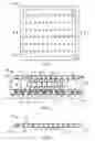
Referring now to FIG. 1, therein is shown a top view of an integrated circuit packaging system 100 in a first embodiment of the present invention. The top view of the integrated circuit packaging system 100 depicts a pre-formed interposer 102, such as a pre-formed through via interposer or a preformed organic interposer. The pre-formed interposer 102 can include a mounting contact 104. An encapsulation 106, such as a cover including an epoxy molding compound, can surround the pre-formed interposer.
For illustrative purposes, the integrated circuit packaging system 100 is shown with the mounting contact 104 in an array configuration, although it is understood that the integrated circuit packaging system 100 can have a different configuration with the mounting contact 104. For example, the mounting contact 104 can form a peripheral configuration or an array configuration with some of the array location depopulated.
Referring now to FIG. 2, therein is shown a cross-sectional view of the integrated circuit packaging system 100 along line 2-2 of FIG. 1. The cross-sectional view of the integrated circuit packaging system 100 depicts the pre-formed interposer 102 within the encapsulation 106. The pre-formed interposer 102 is pre-formed with pre-attached interconnects 208 attached thereto.
The cross-sectional view also depicts an active side 210 of an integrated circuit 212, such as an integrated circuit die or a flip chip, facing a substrate 214, such as a laminated substrate or a printed circuit board.
A device through via 216, such as through silicon via, can include a mounting pad 218 at a non-active side 220 of the integrated circuit 212. The device through via 216 traverses the integrated circuit 212 from the active side 210 to the non-active side 220.
The pre-formed interposer 102 includes a carrier 222, such as a through via interposer or an organic interposer, and the pre-attached interconnects 208, such as solder on pad (SOP) bump or other pre-attached conductive protrusion, attached thereto. The mounting pad 218 can be attached to the pre-attached interconnects 208.
The device through via 216 can be coupled to the substrate 214. A conductive support 224, such as a solder ball, a conductive post, or a conductive column, can be mounted over the substrate 214 and adjacent to the integrated circuit 212.
The integrated circuit 212 can include a device interconnect 226, such as a solder ball, conductive bump, or a conductive post, between the device through via 216 and the substrate 214. The device interconnect 226 can also attach between the active side 210 and the substrate 214 without attaching to the device through via 216.
The encapsulation 106 can be coplanar with the exposed portion of the pre-formed interposer 102. The encapsulation surrounds the pre-attached interconnects 208. The integrated circuit packaging system 100 has the characteristic of robust connection between the pre-attached interconnects 208 and the carrier 222 of the pre-formed interposer 102 such that the mechanical and electrical connection breaks or gaps have been eliminated or reduced. The pre-forming the pre-attached interconnects 208 with the carrier 222 ensure robust bond thereby reducing breakage during the formation of the encapsulation 106.
An external interconnect 228, such as solder balls or conductive bumps, can attach under the substrate 214. The conductive support 224 can be attached to the pre-formed interposer 102. The conductive support 224 can be coupled to the mounting contact 104. The pre-attached interconnects 208 can be attached to the mounting pad 218 coupled to the device through via 216 at the non-active side 220. The pre-attached interconnects 208 can be coupled to the mounting contact 104.
Referring now to FIG. 3, therein is shown a cross-sectional view of the pre-formed interposer 102 having the pre-attached interconnects 208. The pre-formed interposer 102 includes an interposer through via 330, such as an electrical connection structure including a conductive material, copper solder or tungsten. The interposer through via 330 can be a through silicon via or an electrical via. The pre-attached interconnects 208 can be attached to the interposer through via 330.
The interposer through via 330 traverses the pre-formed interposer 102 from a pre-formed interposer non-active side 332 to a pre-formed interposer active side 334. The interposer active side 334 includes active circuitry thereon. The interposer non-active side 332 does not include active circuitry thereon. The interposer through via 330 allows connection from the outside to the interior of the integrated circuit packaging system 100 of FIG. 2 as well as to the external interconnect 228 of FIG. 2.
For illustrative purposes, the pre-formed interposer 102 is shown with the pre-attached interconnects 208 attached to the interposer through via 330, although it is understood that the pre-formed interposer 102 can have a different configuration with the pre-attached interconnects 208. For example, the pre-formed interposer 102 can have the pre-attached interconnects 208 attached to the carrier 222 but not necessarily to the interposer through via 330.
The pre-formed interposer 102 can be formed and tested to ensure reliable mechanical and electrical connection between the carrier 222 and the pre-attached interconnects 208. The pre-attachment ensure the robust connection between the carrier 222 and the pre-attached interconnects 208 is maintained with the mounting over the conductive support 224 of FIG. 2. If interconnects are applied to the non-active side 222 of FIG. 2 instead of pre-attached to the carrier 222, height variations of the conductive support 224 can cause poor or no connection to the carrier 222.
Referring now to FIG. 4, therein is shown a top view of an integrated circuit package-on-package system 400 with the integrated circuit packaging system 100 of FIG. 1 in a second embodiment of the present invention. The top view depicts a mounting device 402, such as an integrated circuit die, a flip chip, or a packaged integrated circuit.
Referring now to FIG. 5, therein is shown a cross-sectional view of the integrated circuit package-on-package system 400 along line 5-5 of FIG. 4. The cross-sectional view depicts the mounting device 402 mounted over the integrated circuit packaging system 100. A mounting interconnect 502 of the mounting device 402 can attach to the pre-formed interposer 102. The mounting interconnect 502 can attach to the interposer through via 330.
It has been discovered that the present invention provides the integrated circuit packaging system having a pre-formed interposer provides reliable connection structure. The integrated circuit packaging system has the characteristics of being formed with the pre-formed interposer. The pre-attached interconnects to the carrier to form the pre-formed interposer reduces or eliminates poor or weak connections between the pre-attached interconnects and the carrier thereby improving reliability during the encapsulating process. Furthermore, the use of a pre-formed interposer provides increased interconnection performance when used with flip chips or other high I/O devices.
It has also been discovered that the present invention provides the integrated circuit packaging system having a dual connectivity and compact footprint. The pre-formed interposer with the interposer though via along with the pre-attached interconnects provide dual connectivity from above and below the integrated packaging system. The device through via and the interposer through via allow the integrated circuit to be electronically coupled to the pre-formed interposer eliminating the need for additional connection structures such as solder balls that can require additional footprint space. Furthermore, the use of a pre-formed interposer can increase the ease of mounting an additional package on top of the integrated circuit package.
Thus, it has been discovered that the integrated circuit packaging of the present invention furnishes important and heretofore unknown and unavailable solutions, capabilities, and functional aspects for dual connectivity with the integrated circuit packaging system.
Referring now to FIG. 6, therein is shown a flow chart of a method 600 of manufacture of an integrated circuit packaging system 100 in a further embodiment of the present invention. The method 600 includes: mounting an integrated circuit, having a device through via and a device interconnect, over a substrate with the device through via traversing the integrated circuit and the device interconnect attached the device through via in a block 602; attaching a conductive support over the substrate with the conductive support adjacent to the integrated circuit in a block 604; providing a pre-formed interposer, having an interposer through via and a pre-attached interconnect, with the pre-attached interconnect attached to the interposer through via in a block 606; mounting the pre-formed interposer over the integrated circuit and the conductive support with the pre-attached interconnect over the device through via in a block 608; and forming an encapsulation over the substrate covering the integrated circuit, the conductive support, and partially covering the pre-formed interposer in a block 610.
The resulting method, process, apparatus, device, product, and/or system is straightforward, cost-effective, uncomplicated, highly versatile and effective, can be surprisingly and unobviously implemented by adapting known technologies, and are thus readily suited for efficiently and economically manufacturing integrated packaging systems.
Another important aspect of the present invention is that it valuably supports and services the historical trend of reducing costs, simplifying systems, and increasing performance.
These and other valuable aspects of the present invention consequently further the state of the technology to at least the next level.
While the invention has been described in conjunction with a specific best mode, it is to be understood that many alternatives, modifications, and variations will be apparent to those skilled in the art in light of the aforegoing description. Accordingly, it is intended to embrace all such alternatives, modifications, and variations that fall within the scope of the included claims. All matters hithertofore set forth herein or shown in the accompanying drawings are to be interpreted in an illustrative and non-limiting sense.
Claims
1. A method of manufacture of an integrated circuit packaging system comprising:
mounting an integrated circuit, having a device through via and a device interconnect, over a substrate with the device through via traversing the integrated circuit and the device interconnect attached the device through via;
attaching a conductive support over the substrate with the conductive support adjacent to the integrated circuit;
providing a pre-formed interposer, having an interposer through via, active circuitry, and a pre-attached interconnect, with the pre-attached interconnect attached to the interposer through via;
mounting the pre-formed interposer over the integrated circuit and the conductive support with the pre-attached interconnect over the device through via; and
forming an encapsulation over the substrate covering the integrated circuit, the conductive support, and partially covering the pre-formed interposer.
2. The method as claimed in claim 1 wherein mounting the pre-formed interposer over the integrated circuit and the conductive support with the pre-attached interconnect over the device through via includes electrically coupling the pre-attached interconnect and the device through via.
3. The method as claimed in claim 1 wherein forming the encapsulation over the substrate covering the integrated circuit, the conductive support, and partially covering the pre-formed interposer includes exposing the interposer through via.
4. The method as claimed in claim 1 wherein forming the encapsulation over the substrate covering the integrated circuit, the conductive support, and partially covering the pre-formed interposer includes forming the encapsulation coplanar with the exposed portion of the pre-formed interposer.
5. The method as claimed in claim 1 wherein providing the pre-formed interposer, having the interposer through via and the pre-attached interconnect, with the pre-attached interconnect attached to the interposer through via includes providing the pre-formed interposer having a pre-attached solder on pad bump.
6. A method of manufacture of an integrated circuit packaging system comprising:
mounting an integrated circuit, having a device through via and a device interconnect, over a substrate with the device through via traversing the integrated circuit and the device interconnect attached the device through via and the substrate;
attaching a conductive support over the substrate with the conductive support adjacent to the integrated circuit;
providing a pre-formed interposer, having an interposer through via, active circuitry, and a pre-attached interconnect, with the pre-attached interconnect attached to the interposer through via;
mounting the pre-formed interposer over the integrated circuit and the conductive support with the pre-attached interconnect over the device through via; and
forming an encapsulation over the substrate covering the integrated circuit, the conductive support, and partially covering the pre-formed interposer with the encapsulation coplanar with the exposed portion of the pre-formed interposer.
7. The method as claimed in claim 6 wherein mounting the pre-formed interposer over the integrated circuit and the conductive support with the pre-attached interconnect over the device through via includes electrically coupling the pre-attached interconnect and the conductive support.
8. The method as claimed in claim 6 wherein providing the pre-formed interposer includes providing an organic interposer.
9. The method as claimed in claim 6 further comprising connecting a mounting device and the device through via.
10. The method as claimed in claim 6 wherein mounting the integrated circuit includes mounting a flip chip.
11. An integrated circuit packaging system comprising:
a substrate;
an integrated circuit, having a device through via and a device interconnect, over the substrate with the device through via traversing the integrated circuit and the device interconnect attached the device through via;
a conductive support over the substrate with the conductive support adjacent to the integrated circuit;
a pre-formed interposer, having an interposer through via, active circuitry, and a pre-attached interconnect, with the pre-attached interconnect attached to the interposer through via including:
the pre-formed interposer having the characteristics of the pre-attached interconnect pre-attached to a carrier of the pre-foamed interposer, and
the pre-formed interposer over the integrated circuit and the conductive support with the pre-attached interconnect over the device through via; and
an encapsulation over the substrate covering the integrated circuit, the conductive support, and partially covering the pre-formed interposer.
12. The system as claimed in claim 11 wherein the pre-attached interconnect is electrically coupled to the device through via.
13. The system as claimed in claim 11 wherein the encapsulation exposes the interposer through via.
14. The system as claimed in claim 11 wherein the encapsulation is coplanar with the exposed portion of the pre-formed interposer.
15. The system as claimed in claim 11 wherein the pre-attached interconnect includes a pre-attached solder on pad bump.
16. The system as claimed in claim 11 wherein:
the device interconnect is attached to the substrate; and
the encapsulation is coplanar with the exposed portion of the pre-formed interposer.
17. The system as claimed in claim 16 wherein the pre-formed interposer is electrically coupled to the conductive support.
18. The system as claimed in claim 16 wherein the pre-formed interposer includes an organic interposer.
19. The system as claimed in claim 16 further comprising a mounting device connected to the device through via.
20. The system as claimed in claim 16 wherein the integrated circuit includes a flip chip.
Images & Drawings included:


Sources:
- United States Patent and Trademark Office - verify current appl. status at the USPTO↗
Similar patent applications:
- » 20100237481
INTEGRATED CIRCUIT PACKAGING SYSTEM WITH DUAL SIDED CONNECTION AND METHOD OF MANUFACTURE THEREOF - » 20110115098
Integrated circuit package system with dual side connection and method for manufacturing thereof - » 20110186994
Integrated circuit packaging system having dual sided connection and method of manufacture thereof - » 20110285009
Integrated circuit packaging system with dual side connection and method of manufacture thereof - » 20110291257
Integrated circuit packaging system with dual side connection and method of manufacture thereof
Recent applications in this class:
- » 20250293134 2025-09-18
SEMICONDUCTOR DEVICE - » 20250285957 2025-09-11
INTERPOSER SUBSTRATE AND SEMICONDUCTOR PACKAGE INCLUDING THE SAME - » 20250273554 2025-08-28
SEMICONDUCTOR PACKAGE - » 20250266342 2025-08-21
MANUFACTURING METHOD FOR THIN WIRING MEMBER, THIN WIRING MEMBER, AND MANUFACTURING METHOD FOR WIRING BOARD - » 20250246530 2025-07-31
CHIP PACKAGE AND MANUFACTURING METHOD THEREOF - » 20250246529 2025-07-31
DISPLAY DEVICE - » 20250218914 2025-07-03
PACKAGE WITH COMPONENT-CARRYING INTERMEDIATE STRUCTURE AND ADDITIONAL CARRIER HAVING REFERENCE POTENTIAL STRUCTURE - » 20250210494 2025-06-26
SEMICONDUCTOR PACKAGE - » 20250210493 2025-06-26
SEMICONDUCTOR DEVICE - » 20250210492 2025-06-26
POWER MODULE, PRODUCTION METHOD THEREOF, AND POWER DEVICE
Recent applications for this Assignee:
- » 20160351486 2016-12-01
Semiconductor device and method of forming substrate including embedded component with symmetrical structure - » 20160300817 2016-10-13
Semiconductor device and method of forming a package in-fan out package - » 20160300797 2016-10-13
Double-sided semiconductor package and dual-mold method of making same - » 20160276307 2016-09-22
Semiconductor device and method of forming PoP semiconductor device with RDL over top package - » 20160276238 2016-09-22
Semiconductor device and method of forming supporting layer over semiconductor die in thin fan-out wafer level chip scale package - » 20160233168 2016-08-11
Semiconductor device and method of forming 3D dual side die embedded build-up semiconductor package - » 20160218089 2016-07-28
Semiconductor device and method of forming WLCSP with semiconductor die embedded within interconnect structure - » 20160214857 2016-07-28
Semiconductor device and method of forming MEMS package - » 20160197059 2016-07-07
Semiconductor device and method of forming shielding layer over integrated passive device using conductive channels - » 20160197022 2016-07-07
Semiconductor device and method of forming sacrificial adhesive over contact pads of semiconductor die