System and method to reduce the bondwire/trace inductance
US20110006440A1
2011-01-13
12/500,046
2009-07-09
✅ Patent granted
US 8,021,973 B2
2011-09-20
-
-
Quoc D Hoang
2030-03-10
Abstract:
A method and system for reducing the inductance on an integrated circuit. The method and system comprises providing a first differential line, including a first input and a first output, the first differential line including at least two bondwire traces which are coupled in parallel. The method and system also comprises providing a second differential line including a second input and a second output, the second differential line including at least two bondwire traces which are coupled in parallel, the first differential line being of opposite polarity to the second differential line. The method and system further comprises cross-coupling of the first input with the second input and the first output with the second output to reduce the inductance caused by bondwire traces. A technique in accordance with the invention uses the coupling factor K to help to further reduce the inductance. By changing the input ordering of differential bondwires/traces, the bondwire/trace magnetic coupling factor K can be used to reduce the line inductance.
Assignee:
- RALINK TECHNOLOGY (SINGAPORE) CORPORATION 8 🇸🇬 Singapore, Singapore
Interested in similar patents?
Get notified when new applications in this technology area are published.
Classification:
H01L23/645 » CPC main
Details of semiconductor or other solid state devices; Structural electrical arrangements for semiconductor devices not otherwise provided for, e.g. in combination with batteries; Impedance arrangements Inductive arrangements
H01L23/66 » CPC further
Details of semiconductor or other solid state devices; Structural electrical arrangements for semiconductor devices not otherwise provided for, e.g. in combination with batteries; Impedance arrangements High-frequency adaptations
H01L24/49 » CPC further
Arrangements for connecting or disconnecting semiconductor or solid-state bodies; Methods or apparatus related thereto; Means for bonding being attached to, or being formed on, the surface to be connected, e.g. chip-to-package, die-attach, "first-level" interconnects; Manufacturing methods related thereto; Wire connectors; Manufacturing methods related thereto; Structure, shape, material or disposition of the wire connectors after the connecting process of a plurality of wire connectors
H01L24/48 » CPC further
Arrangements for connecting or disconnecting semiconductor or solid-state bodies; Methods or apparatus related thereto; Means for bonding being attached to, or being formed on, the surface to be connected, e.g. chip-to-package, die-attach, "first-level" interconnects; Manufacturing methods related thereto; Wire connectors; Manufacturing methods related thereto; Structure, shape, material or disposition of the wire connectors after the connecting process of an individual wire connector
H01L2223/6638 » CPC further
Details relating to semiconductor or other solid state devices covered by the group; Structural electrical arrangements for semiconductor devices not otherwise provided for; Impedance arrangements; High-frequency adaptations; High-frequency electrical connections Differential pair signal lines
H01L2223/6644 » CPC further
Details relating to semiconductor or other solid state devices covered by the group; Structural electrical arrangements for semiconductor devices not otherwise provided for; Impedance arrangements; High-frequency adaptations Packaging aspects of high-frequency amplifiers
H01L2224/48 » CPC further
Indexing scheme for arrangements for connecting or disconnecting semiconductor or solid-state bodies and methods related thereto as covered by; Means for bonding being attached to, or being formed on, the surface to be connected, e.g. chip-to-package, die-attach, "first-level" interconnects; Manufacturing methods related thereto; Wire connectors; Manufacturing methods related thereto; Structure, shape, material or disposition of the wire connectors after the connecting process of an individual wire connector
H01L2924/01019 » CPC further
Indexing scheme for arrangements or methods for connecting or disconnecting semiconductor or solid-state bodies as covered by; Chemical elements Potassium [K]
H01L2924/01033 » CPC further
Indexing scheme for arrangements or methods for connecting or disconnecting semiconductor or solid-state bodies as covered by; Chemical elements Arsenic [As]
H01L2924/01082 » CPC further
Indexing scheme for arrangements or methods for connecting or disconnecting semiconductor or solid-state bodies as covered by; Chemical elements Lead [Pb]
H01L2924/14 » CPC further
Indexing scheme for arrangements or methods for connecting or disconnecting semiconductor or solid-state bodies as covered by; Details of semiconductor or other solid state devices to be connected; Device type Integrated circuits
H01L2924/19042 » CPC further
Indexing scheme for arrangements or methods for connecting or disconnecting semiconductor or solid-state bodies as covered by; Details of hybrid assemblies other than the semiconductor or other solid state devices to be connected; Structure; Component type being an inductor
H01L2924/30107 » CPC further
Indexing scheme for arrangements or methods for connecting or disconnecting semiconductor or solid-state bodies as covered by; Technical effects; Electrical effects Inductance
H01L2924/00014 » CPC further
Indexing scheme for arrangements or methods for connecting or disconnecting semiconductor or solid-state bodies as covered by; Technical content checked by a classifier the subject-matter covered by the group, the symbol of which is combined with the symbol of this group, being disclosed without further technical details
H01L2224/45099 » CPC further
Indexing scheme for arrangements for connecting or disconnecting semiconductor or solid-state bodies and methods related thereto as covered by; Means for bonding being attached to, or being formed on, the surface to be connected, e.g. chip-to-package, die-attach, "first-level" interconnects; Manufacturing methods related thereto; Wire connectors; Manufacturing methods related thereto; Structure, shape, material or disposition of the wire connectors prior to the connecting process of an individual wire connector; Core members of the connector Material
H01L23/522 IPC
Details of semiconductor or other solid state devices; Arrangements for conducting electric current within the device in operation from one component to another, i.e. interconnections, e.g. wires, lead frames including external interconnections consisting of a multilayer structure of conductive and insulating layers inseparably formed on the semiconductor body
H01L21/60 IPC
Processes or apparatus adapted for the manufacture or treatment of semiconductor or solid state devices or of parts thereof; Manufacture or treatment of semiconductor devices or of parts thereof the devices having at least one potential-jump barrier or surface barrier, e.g. PN junction, depletion layer or carrier concentration layer; Assembly of semiconductor devices using processes or apparatus not provided for in a single one of the subgroups - , e.g. sealing of a cap to a base of a container Attaching or detaching leads or other conductive members, to be used for carrying current to or from the device in operation
H01L21/44 IPC
Processes or apparatus adapted for the manufacture or treatment of semiconductor or solid state devices or of parts thereof; Manufacture or treatment of semiconductor devices or of parts thereof the devices having at least one potential-jump barrier or surface barrier, e.g. PN junction, depletion layer or carrier concentration layer the devices having semiconductor bodies not provided for in groups, , , and with or without impurities, e.g. doping materials Manufacture of electrodes on semiconductor bodies using processes or apparatus not provided for in groups -
Description
FIELD OF THE INVENTION
The present invention relates generally to integrated circuits and more specifically to reducing the parasitic inductances for such circuits.
BACKGROUND OF THE INVENTION
Integrated circuits and/or packages include a plurality of traces for coupling different components together. The chip package bondwires (or onchip or on-board traces) usually has a large inductance. At high frequencies, this large inductance will cause a large RF swing. Furthermore, the large inductance will make the matching wideband applications more difficult.
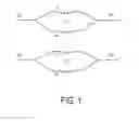
The conventional way to reduce the inductance of the traces is to parallel multiple bondwires/traces. In this traditional approach, the magnetic coupling factor K has a negative effect on reducing the parallel bondwires/traces inductance. FIG. 1 illustrates the conventional technique to reduce the bondwire/trace inductance. L1-L4 are the chip bondwires, on-chip layout trace or board traces. In the case that L1-L4 are bondwires, P1 and P2 are connected to bondpads on die and P3 and P4 are connected to package pins. In the case that L1-L4 are differential traces on chip or on board, P1 and P2 are differential inputs and P3 and P4 are differential outputs. The conventional way to reduce the inductance is to parallel L1 and L2 (or L3 and L4) to make the effective inductance from P1 to P3 (or P2 to P4) smaller.
Let L1=L2=L3=L4=L, and inductance coupling factor is K. If coupling factor K=0, the effective inductance from P1 to P3 (or P2 to P4) Lpp=L1*L2/9L2+L2)=L/2. If K is not 0, the magnetic fields of the bondwires/traces will strengthen each other and the Lpp>L/2. Accordingly, the larger K is, the larger the Lpp. So the reduction from parallel bondwire approach does necessarily reduce the inductance.
Therefore the traditional method in some instances sometimes does not reduce the inductance. The larger K is, the larger the inductance. Accordingly, what is needed is a system and method to overcome the above-identified issues. The present invention addresses such a need.
SUMMARY OF THE INVENTION
A method and system is disclosed for reducing the inductance on an integrated circuit. The method and system comprise providing a first differential line, including a first input and a first output, the first differential line including at least two bondwire traces which are coupled in parallel. The method and system also comprise providing a second differential line including a second input and a second output, the second differential line including at least two bondwire traces which are coupled in parallel, the first differential line being of opposite polarity to the second differential line. The method and system further comprise cross-coupling of the first input with the second input and the first output with the second output to reduce the inductance caused by bondwire traces.
A technique in accordance with the present invention uses the coupling factor K to help to further reduce the inductance. By changing the input ordering of differential bondwires/traces, the bondwire/trace magnetic coupling factor K can be used to reduce the line inductance.
BRIEF DESCRIPTION OF THE DRAWINGS
FIG. 1 illustrates a conventional system to reduce the bondwire/layout trace inductance.
FIG. 2 illustrates a system in accordance with the present invention to reduce the bondwire/layout trace inductance.
FIG. 3 shows simulation results of an approach in accordance with the present invention and the conventional approach.
FIG. 4 illustrates the use of system in accordance with the present invention for power amplifier output matching.
FIG. 5 illustrates the system in accordance with the present invention extended to a more general use.
DETAILED DESCRIPTION
The present invention relates generally to integrated circuits and more specifically to reducing the parasitic inductances for such circuits. The following description is presented to enable one of ordinary skill in the art to make and use the invention and is provided in the context of a patent application and its requirements. Various modifications to the preferred embodiments and the generic principles and features described herein will be readily apparent to those skilled in the art. Thus, the present invention is not intended to be limited to the embodiments shown, but is to be accorded the widest scope consistent with the principles and features described herein.
In an embodiment the inputs and outputs of the package are cross coupled. In this way, the coupling factor K will help to reduce the inductance rather than increase the inductance, because the magnetic fields of the adjacent bondwires/traces will cancel each other. To describe the features of the present invention refer now to the following description in conjunction with accompanying Figures.
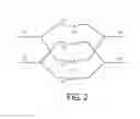
FIG. 2 illustrates a method and system in accordance with the present invention to reduce the bondwire/layout trace inductance. As is seen, input P1′ is cross coupled with input P2′. Similarly, output P3′ is coupled with output P4′.
If coupling factor K=0, the effective inductance from P1 to P3 (or P2 to P4) is still Lpp=L1*L2/(L1+L2)=L/2. However, if K is not 0, the Lpp<L/2. In this example, Lpp∝ (1−k), where 0<k<1. As can be seen from this equation, the larger K is, the smaller Lpp. So the inductor coupling factor K will help reduce the inductance when inputs and outputs are cross complex.
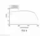
FIG. 3 shows the simulation results of an approach in accordance with the present invention and the conventional approach. Y axis is the effective inductance Leff from P1 to P3 (or P2 to P4). Assuming L1=L2=L3=L4=6 nH. The coupling factor K range is between 0 to 0.6. At K=0, both approaches provide the same effective inductance (Leff)=3 nH. As K increases, the new approach provides a much smaller inductance than the conventional approach.
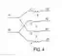
FIG. 4 illustrates the application when used for power amplifier (PA) output matching. P1″ and P2″ are connected to bondpads on chip and those pads are connected to the drains of the PA device. The bondwires L1″ and L4″ are used as radio frequency choce to supply the DC current to PA and they are connected to the DC supply (Vdd) Pin on package. P3″ and P4″ are the two package pins connecting to the output matching network on board. The cross connection of P1″ and P2″ will largely reduce the effective inductance between P1″ and P3″ (or P2″ and P4″). It means the PA has a wideband matching and is less sensitive to components variation.
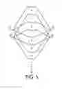
FIG. 5 is a diagram for the more general case wherein there are N bondwires/traces with cross coupled inputs and outputs. Accordingly, as is seen a plurality of inputs and outputs can be cross coupled to further reduce the magnetic coupling.
Although the present invention has been described in accordance with the embodiments shown, one of ordinary skill in the art will readily recognize that there could be variations to the embodiments and those variations would be within the spirit and scope of the present invention. Accordingly, many modifications may be made by one of ordinary skill in the art without departing from the spirit and scope of the appended claims.
Claims
What is claimed is:1. A method for reducing the inductance on an integrated circuit comprising:
providing a first differential line, including a first input and a first output, the first differential line including at least two bondwire traces which are coupled in parallel,
providing a second differential line including a second input and a second output, the second differential line including at least two bondwire traces which are coupled in parallel, the first differential line being of opposite polarity to the second differential line; and
cross-coupling of the first input with the second input and the first output with the second output to reduce the inductance caused by bondwire traces.
2. The method of claim 1 wherein the first and second inputs are coupled to bondpads on a die and the first and second outputs are coupled to package pins.
3. The method of claim 1 wherein the first and second inputs are coupled to bondpads on a die and the first and second outputs are two pins coupled to an output power matching network.
4. A system comprising:
a first differential line, including a first input and a first output, the first differential line including at least two bondwire traces which are coupled in parallel,
a second differential line including a second input and a second output, the second differential line including at least two bondwire traces which are coupled in parallel, the first differential line being of opposite polarity to the second differential line; wherein the first input is cross-coupled with the second input and the first output is cross-coupled with the second output to reduce the inductance caused by bondwire traces.
5. The system of claim 4 wherein the first and second inputs are coupled to bondpads on a die and the first and second outputs are coupled to package pins.
6. The system of claim 4 wherein the first and second inputs are coupled to bondpads on a die and the first and second outputs are two pins coupled to an output power matching network.
Images & Drawings included:
Sources:
- United States Patent and Trademark Office - verify current appl. status at the USPTO↗
Recent applications in this class:
- » 20250293183 2025-09-18
SEMICONDUCTOR DEVICE - » 20250293182 2025-09-18
COMPACT DEVICE FOR IMPROVED HIGH-SPEED SIGNAL INTEGRITY - » 20250273605 2025-08-28
SEMICONDUCTOR DEVICE - » 20250253271 2025-08-07
INTEGRATING HIGH PERMEABILITY MATERIAL IN SOLDER BALL CONNECTION - » 20250233088 2025-07-17
VERTICAL POWER DELIVERY IN SPACE-CONSTRAINED SYSTEM-ON-PACKAGE - » 20250226337 2025-07-10
EMBEDDED INDUCTORS AND INTEGRATED VOLTAGE REGULATORS FOR PACKAGED SEMICONDUCTOR DEVICES - » 20250218984 2025-07-03
ENCAPSULATION TECHNIQUES FOR COMPONENTS EMBEDDED IN A CORE LAYER OF A PACKAGE SUBSTRATE - » 20250183202 2025-06-05
SEMICONDUCTOR PACKAGE DEVICE WITH INTEGRATED INDUCTOR AND MANUFACTURING METHOD THEREOF - » 20250183201 2025-06-05
PANEL SCALE PACKAGING OF A PLURALITY OF TRANSFORMER DEVICES FOR REDUCED PARASITIC INDUCTANCE - » 20250149471 2025-05-08
ELECTRONIC PACKAGE AND MANUFACTURING METHOD THEREOF
Recent applications for this Assignee:
- » 20110143690 2011-06-16
Method and system for integrating transmit switch functionality in a WLAN radio transceiver - » 20110007848 2011-01-13
METHOD FOR CALIBRATING IQ MATCHING OF RECEIVER - » 20100296554 2010-11-25
METHOD AND SYSTEM FOR DETECTING DATA FROM MULTIPLE ANTENNAS - » 20100289541 2010-11-18
Digital phase-locked loop circuit including a phase delay quantizer and method of use - » 20100289539 2010-11-18
Method and system of optimizing a control system using low voltage and high-speed switching - » 20100248669 2010-09-30
Dual-band transceiver - » 20090224831 2009-09-10
Cancellation of common mode oscillation in RF circuits