Electronic part and method of manufacturing the same
US20110042824A1
2011-02-24
12/857,893
2010-08-17
✅ Patent granted
US 8,368,230 B2
2013-02-05
-
-
Nathan Ha
Squire Sanders (US) LLP
2030-08-17
Abstract:
A multi-chip module includes a package board, a plurality of chips, and a wiring board. The plurality of chips are horizontally disposed on the package board. The plurality of chips are electrically connected with the package board, and respectively provided with via holes which penetrate through the plurality of chips. The plurality of chips are respectively provided with circuits at surfaces facing the package board. The wiring board is disposed on an opposite side to the package board across the plurality of chips. The wiring board includes a wiring pattern which is electrically connecting adjacent chips one another. The circuit is electrically connected to the wiring pattern through the via holes.
Assignee:
- FUJITSU LIMITED 18,021 🇯🇵 Kawasaki-shi, Japan
- FUJITSU LIMITED 26,672 🇯🇵 Kawasaki, Japan
Applicant:
Interested in similar patents?
Get notified when new applications in this technology area are published.
Classification:
H01L2924/0002 » CPC further
Indexing scheme for arrangements or methods for connecting or disconnecting semiconductor or solid-state bodies as covered by; Technical content checked by a classifier Not covered by any one of groups , and
H01L23/147 » CPC main
Details of semiconductor or other solid state devices; Mountings, e.g. non-detachable insulating substrates characterised by the material or its electrical properties Semiconductor insulating substrates
H01L21/76898 » CPC further
Processes or apparatus adapted for the manufacture or treatment of semiconductor or solid state devices or of parts thereof; Manufacture or treatment of devices consisting of a plurality of solid state components formed in or on a common substrate or of parts thereof; Manufacture of integrated circuit devices or of parts thereof; Manufacture of specific parts of devices defined in group; Applying interconnections to be used for carrying current between separate components within a device comprising conductors and dielectrics formed through a semiconductor substrate
H01L23/481 » CPC further
Details of semiconductor or other solid state devices; Arrangements for conducting electric current to or from the solid state body in operation, e.g. leads, terminal arrangements ; Selection of materials therefor Internal lead connections, e.g. via connections, feedthrough structures
H01L23/49822 » CPC further
Details of semiconductor or other solid state devices; Arrangements for conducting electric current to or from the solid state body in operation, e.g. leads, terminal arrangements ; Selection of materials therefor consisting of soldered constructions; Leads, on insulating substrates, Multilayer substrates
H01L23/49827 » CPC further
Details of semiconductor or other solid state devices; Arrangements for conducting electric current to or from the solid state body in operation, e.g. leads, terminal arrangements ; Selection of materials therefor consisting of soldered constructions; Leads, on insulating substrates, Via connections through the substrates, e.g. pins going through the substrate, coaxial cables
H01L23/49838 » CPC further
Details of semiconductor or other solid state devices; Arrangements for conducting electric current to or from the solid state body in operation, e.g. leads, terminal arrangements ; Selection of materials therefor consisting of soldered constructions; Leads, on insulating substrates, Geometry or layout
H01L24/14 » CPC further
Arrangements for connecting or disconnecting semiconductor or solid-state bodies; Methods or apparatus related thereto; Means for bonding being attached to, or being formed on, the surface to be connected, e.g. chip-to-package, die-attach, "first-level" interconnects; Manufacturing methods related thereto; Bump connectors ; Manufacturing methods related thereto; Structure, shape, material or disposition of the bump connectors prior to the connecting process of a plurality of bump connectors
H01L24/81 » CPC further
Arrangements for connecting or disconnecting semiconductor or solid-state bodies; Methods or apparatus related thereto; Methods for connecting semiconductor or other solid state bodies using means for bonding being attached to, or being formed on, the surface to be connected using a bump connector
H01L24/95 » CPC further
Arrangements for connecting or disconnecting semiconductor or solid-state bodies; Methods or apparatus related thereto; Batch processes at chip-level, i.e. with connecting carried out on a plurality of singulated devices, i.e. on diced chips
H01L25/0655 » CPC further
Assemblies consisting of a plurality of individual semiconductor or other solid state devices ; Multistep manufacturing processes thereof all the devices being of a type provided for in the same subgroup of groups - , e.g. assemblies of rectifier diodes the devices not having separate containers the devices being of a type provided for in group the devices being arranged next to each other
H01L24/13 » CPC further
Arrangements for connecting or disconnecting semiconductor or solid-state bodies; Methods or apparatus related thereto; Means for bonding being attached to, or being formed on, the surface to be connected, e.g. chip-to-package, die-attach, "first-level" interconnects; Manufacturing methods related thereto; Bump connectors ; Manufacturing methods related thereto; Structure, shape, material or disposition of the bump connectors prior to the connecting process of an individual bump connector
H01L2224/0401 » CPC further
Indexing scheme for arrangements for connecting or disconnecting semiconductor or solid-state bodies and methods related thereto as covered by; Means for bonding being attached to, or being formed on, the surface to be connected, e.g. chip-to-package, die-attach, "first-level" interconnects; Manufacturing methods related thereto; Bonding areas; Manufacturing methods related thereto; Structure, shape, material or disposition of the bonding areas prior to the connecting process Bonding areas specifically adapted for bump connectors, e.g. under bump metallisation [UBM]
H01L2224/13099 » CPC further
Indexing scheme for arrangements for connecting or disconnecting semiconductor or solid-state bodies and methods related thereto as covered by; Means for bonding being attached to, or being formed on, the surface to be connected, e.g. chip-to-package, die-attach, "first-level" interconnects; Manufacturing methods related thereto; Bump connectors; Manufacturing methods related thereto; Structure, shape, material or disposition of the bump connectors prior to the connecting process of an individual bump connector; Core members of the bump connector Material
H01L2224/1403 » CPC further
Indexing scheme for arrangements for connecting or disconnecting semiconductor or solid-state bodies and methods related thereto as covered by; Means for bonding being attached to, or being formed on, the surface to be connected, e.g. chip-to-package, die-attach, "first-level" interconnects; Manufacturing methods related thereto; Bump connectors; Manufacturing methods related thereto; Structure, shape, material or disposition of the bump connectors prior to the connecting process of a plurality of bump connectors; Structure Bump connectors having different sizes, e.g. different diameters, heights or widths
H01L2224/16 » CPC further
Indexing scheme for arrangements for connecting or disconnecting semiconductor or solid-state bodies and methods related thereto as covered by; Means for bonding being attached to, or being formed on, the surface to be connected, e.g. chip-to-package, die-attach, "first-level" interconnects; Manufacturing methods related thereto; Bump connectors; Manufacturing methods related thereto; Structure, shape, material or disposition of the bump connectors after the connecting process of an individual bump connector
H01L2224/274 » CPC further
Indexing scheme for arrangements for connecting or disconnecting semiconductor or solid-state bodies and methods related thereto as covered by; Means for bonding being attached to, or being formed on, the surface to be connected, e.g. chip-to-package, die-attach, "first-level" interconnects; Manufacturing methods related thereto; Layer connectors, e.g. plate connectors, solder or adhesive layers; Manufacturing methods related thereto; Manufacturing methods by blanket deposition of the material of the layer connector
H01L2224/73204 » CPC further
Indexing scheme for arrangements for connecting or disconnecting semiconductor or solid-state bodies and methods related thereto as covered by; Means for bonding being of different types provided for in two or more of groups; Location after the connecting process on the same surface; Bump and layer connectors the bump connector being embedded into the layer connector
H01L2224/73253 » CPC further
Indexing scheme for arrangements for connecting or disconnecting semiconductor or solid-state bodies and methods related thereto as covered by; Means for bonding being of different types provided for in two or more of groups; Location after the connecting process on different surfaces Bump and layer connectors
H01L2224/81191 » CPC further
Indexing scheme for arrangements for connecting or disconnecting semiconductor or solid-state bodies and methods related thereto as covered by; Methods for connecting semiconductor or other solid state bodies using means for bonding being attached to, or being formed on, the surface to be connected using a bump connector; Arrangement of the bump connectors prior to mounting wherein the bump connectors are disposed only on the semiconductor or solid-state body
H01L2224/81194 » CPC further
Indexing scheme for arrangements for connecting or disconnecting semiconductor or solid-state bodies and methods related thereto as covered by; Methods for connecting semiconductor or other solid state bodies using means for bonding being attached to, or being formed on, the surface to be connected using a bump connector; Arrangement of the bump connectors prior to mounting Lateral distribution of the bump connectors
H01L2224/81801 » CPC further
Indexing scheme for arrangements for connecting or disconnecting semiconductor or solid-state bodies and methods related thereto as covered by; Methods for connecting semiconductor or other solid state bodies using means for bonding being attached to, or being formed on, the surface to be connected using a bump connector; Bonding techniques Soldering or alloying
H01L2924/01005 » CPC further
Indexing scheme for arrangements or methods for connecting or disconnecting semiconductor or solid-state bodies as covered by; Chemical elements Boron [B]
H01L2924/01006 » CPC further
Indexing scheme for arrangements or methods for connecting or disconnecting semiconductor or solid-state bodies as covered by; Chemical elements Carbon [C]
H01L2924/01029 » CPC further
Indexing scheme for arrangements or methods for connecting or disconnecting semiconductor or solid-state bodies as covered by; Chemical elements Copper [Cu]
H01L2924/01033 » CPC further
Indexing scheme for arrangements or methods for connecting or disconnecting semiconductor or solid-state bodies as covered by; Chemical elements Arsenic [As]
H01L2924/01074 » CPC further
Indexing scheme for arrangements or methods for connecting or disconnecting semiconductor or solid-state bodies as covered by; Chemical elements Tungsten [W]
H01L2924/01078 » CPC further
Indexing scheme for arrangements or methods for connecting or disconnecting semiconductor or solid-state bodies as covered by; Chemical elements Platinum [Pt]
H01L2924/15151 » CPC further
Indexing scheme for arrangements or methods for connecting or disconnecting semiconductor or solid-state bodies as covered by; Details of package parts other than the semiconductor or other solid state devices to be connected; Die mounting substrate; Shape the die mounting substrate comprising an aperture, e.g. for underfilling, outgassing, window type wire connections
H01L2924/15311 » CPC further
Indexing scheme for arrangements or methods for connecting or disconnecting semiconductor or solid-state bodies as covered by; Details of package parts other than the semiconductor or other solid state devices to be connected; Die mounting substrate; Connection portion the connection portion being formed only on the surface of the substrate opposite to the die mounting surface being a ball array, e.g. BGA
H01L2924/10253 » CPC further
Indexing scheme for arrangements or methods for connecting or disconnecting semiconductor or solid-state bodies as covered by; Details of semiconductor or other solid state devices to be connected; Material of the semiconductor or solid state bodies; Semiconducting materials; Elemental semiconductors, i.e. Group IV Silicon [Si]
H01L2924/00 » CPC further
Indexing scheme for arrangements or methods for connecting or disconnecting semiconductor or solid-state bodies as covered by
H01L2924/014 » CPC further
Indexing scheme for arrangements or methods for connecting or disconnecting semiconductor or solid-state bodies as covered by; Alloys Solder alloys
H01L23/538 IPC
Details of semiconductor or other solid state devices; Arrangements for conducting electric current within the device in operation from one component to another, i.e. interconnections, e.g. wires, lead frames the interconnection structure between a plurality of semiconductor chips being formed on, or in, insulating substrates
H01L21/60 IPC
Processes or apparatus adapted for the manufacture or treatment of semiconductor or solid state devices or of parts thereof; Manufacture or treatment of semiconductor devices or of parts thereof the devices having at least one potential-jump barrier or surface barrier, e.g. PN junction, depletion layer or carrier concentration layer; Assembly of semiconductor devices using processes or apparatus not provided for in a single one of the subgroups - , e.g. sealing of a cap to a base of a container Attaching or detaching leads or other conductive members, to be used for carrying current to or from the device in operation
H01L25/03 IPC
Assemblies consisting of a plurality of individual semiconductor or other solid state devices ; Multistep manufacturing processes thereof all the devices being of a type provided for in the same subgroup of groups - , e.g. assemblies of rectifier diodes
Description
CROSS-REFERENCE TO RELATED APPLICATIONS
This application is based upon and claims the benefit of priority of the prior Japanese Patent Application No. 2009-191280, filed on Aug. 20, 2009, the entire contents of which are incorporated herein by reference.
FIELD
Embodiments discussed herein are related to a multi-chip module and a method of manufacturing the same.
BACKGROUND
There is known a semiconductor chip module called multi-chip module (MCM). In a conventional multi-chip module, multiple silicon chips which have been manufactured by separate processes are horizontally packaged onto a unifying substrate. Bare silicon chips are exposed, and are respectively connected with each other through a wiring formed on a ceramic or a build-up board (See for example Japanese Unexamined Patent Publication No. 6-283661).
However, in order to secure a substantial channel area in response to the wiring specification of the ceramic or the build-up board in JP-A-6-283661, a clearance between adjacent chips has to be large.
Additionally, since the large clearance between the chips elongates a wiring length between the chips, it may be difficult to transmit data at high rates between the chips such as large-scale integration (LSI) chips. Further, when the wiring length is elongated, the driver installed in the LSI has to be changed into another lager driver, and the size of the LSI may be accordingly larger. Furthermore, the provision of a large number of channels in the board is limited by the wiring specification.
On the other hand, recently, there has been developed a board having fine wirings such as a build-up board (See for example Japanese Unexamined Patent Publication No. 2001-94033). However, to manufacture the build-up board, a specific process or an equipment is additionally needed. Thus, its cost may be increased.
SUMMARY
According to an aspect of the embodiments, a multi-chip module includes a package board, a plurality of chips, and a wiring board. The plurality of chips are horizontally disposed on the package board. The plurality of chips are electrically connected with the package board, and respectively provided with via holes which penetrate through the plurality of chips. The plurality of chips are respectively provided with circuits at surfaces facing the package board. The wiring board is disposed on an opposite side to the package board across the plurality of chips. The wiring board includes a wiring pattern which is electrically connecting adjacent chips one another. The circuit is electrically connected to the wiring pattern through the via holes.
The object and advantages of the invention will be realized and attained by means of the elements and combinations particularly pointed out in the claims.
It is to be understood that both the foregoing general description and the following detailed description are exemplary and explanatory and are not restrictive of the invention, as claimed.
BRIEF DESCRIPTION OF DRAWINGS
FIG. 1 is an cross sectional view of schematically illustrating a multi-chip module according to an embodiment;
FIG. 2 is a plain view of an arrangement of LSI chips;
FIG. 3 is a partially enlarged view of a silicon interposer;
FIGS. 4A to 4E are explanatory views of a method of manufacturing the multi-chip module;
FIGS. 5A to 5C are explanatory views of the method of manufacturing the multi-chip module; and
FIGS. 6A and 6B are explanatory views of the method of manufacturing the multi-chip module.
DESCRIPTION OF EMBODIMENTS
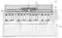
The following description will be given of a multi-chip module and a method of manufacturing the multi-chip module according to an embodiment, with reference to FIGS. 1 to 6B. FIG. 1 is a cross sectional view of schematically illustrating a multi-chip module 100 according to an embodiment. The multi-chip module 100 is secured on a motherboard 200 through solder bumps 210, as illustrated in FIG. 1.
The multi-chip module 100 includes: a package board 10; four LSI chips 30A to 30D as chips; a silicon interposer 20 as a wiring board; and a heat spreader 50. The 30C and 30D are illustrated in FIG. 2.
The package board 10 is called as build-up board. The package board 10 is a multilayer board including: a board having wiring layers and called core board; and wiring layers formed on front and rear surfaces of the board. For example, the core board has four wiring layers, and the first to third wiring layers are provided on the front and rear surfaces of the board. The wiring formed in the package board 10 connects the motherboard 200 with the LSI chips 30A to 30D. Examples of the material of the board may be an epoxy resin, polyimide, or ceramic. An example of the material of the wiring is copper.
Each of the LSI chips 30A to 30D includes: a chip forming member composed of a silicon wafer; and a thin film 31 formed on the chip forming member, wiring patterns being formed in the thin film 31. Hereinafter, the thin films 31 of the LSI chips 30A to 30D are referred to as thin film circuits 31. The LSI chips 30A to 30D are secured on the package board 10 through the solder bumps 140. The vicinity of the solder bumps 140, that is, the clearance or pitch between the LSI chips 30A to 30D and the package board 10, is sealed with a resin (underfill material) 38.
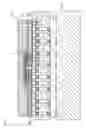
FIG. 2 schematically illustrates a positional relationship between the LSI chips 30A to 30D and the silicon interposer 20. As illustrated in FIG. 2, the LSI chips 30A to 30D are closely arranged to each other. Plural via holes 32 are provided at the corners, of the LSI chips 30A to 30D, close to each other, and penetrate through the LSI chips 30A to 30D, as illustrated in FIG. 1. For example, the via holes 32 are arranged at about 50 μm intervals. The via holes 32 are plated (filled) with a metal such as a copper. Pads 144 are respectively provided on upper ends of the via holes 32. Solder bumps 28 are respectively provided at upper sides of the pads 144.
The silicon interposer 20 has a size so as to cover the area where the via holes 32 are provided in the LSI chips 30A to the 30D, as illustrated in FIGS. 1 and 2. For example, the size of the silicon interposer 20 is 10 mm by 10 mm. The silicon interposer 20 includes: a silicon board; and an insulting layer formed on the silicon board. A wiring pattern is formed in the insulting layer by a semiconductor manufacture equipment such as a semiconductor exposure apparatus. FIG. 3 is an enlarged view of the silicon interposer 20. The wiring pattern mentioned above is represented with a reference numeral 26a. The wiring patterns 26a connect the LSI chips 30A with the LSI chips 30B and 30D, and connect the 30C with the LSI chips 30B and 30D.
Returning to FIG. 1, the heat spreader 50 is provided to cover the upper surfaces of the LSI chips 30A to 30D and that of the silicon interposer 20 through a thermal injection material (TIM) 40. For example, the heat spreader 50 is made of a material such as copper, and has a function for radiating the heat generated in the LSI chips 30A to 30D.
In such a multi-chip module 100 configured above, the LSI chips 30A to 30D, which are electrically connected with the package board 10, are connected with each other through the wiring patterns 26a of the silicon interposer 20. Further, the thin film circuits 31 of the LSI chips 30A to 30D are electrically connected with the wiring patterns 26a of the silicon interposer 20 through the via holes 32. Thus, it is possible for the LSI chips 30A and 30D to be electrically connected with the package board 10 and electrically connected with each other through the silicon interposer 20.
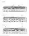
Next, a method of manufacturing the multi-chip module 100 will be described with reference to FIGS. 4A to 6B.
First, a chip forming member 30′ for eventually becoming the LSI chips 30A to 30B is manufactured with reference to FIGS. 4A to 4E. In the production of the chip forming member 30′, a silicon wafer W is prepared as illustrated in FIG. 4. The silicon wafer W has a predetermined thickness equal to or greater than each of the thicknesses of the LSI chips 30A to 30D. Next, holes 132 for eventually becoming the via holes 32 are formed by etching as illustrated in FIG. 4B. Then, as illustrated in FIG. 4C, the holes 132 of the silicon wafer W are plated and filled with a metal such as copper, so the thin film circuit 31 is formed. In the formation of the thin film circuit 31, a semiconductor manufacture equipment such as a semiconductor exposure apparatus is used. Then, pads 138 for signals are formed on the thin film circuit 31 by plating a metal such as a copper, as illustrated in FIG. 4D. The silicon wafer W has to be diced into a desired size, after or before the process illustrated in FIG. 4D is accomplished. The diced silicon wafer W becomes the chip forming member 30′. Then, the solder bumps 140 are respectively formed on the pads 138 of the chip forming member 30′, as illustrated in FIG. 4E. Additionally, the silicon wafer W may be diced after the solder bumps 140 illustrated in FIG. 4E are formed.
Next, plural (four, in this case) chip forming members 30′ are horizontally mounted on the package board 10 in the same arrangement with the LSI chips 30A to 30D illustrated in FIG. 2. For example, the clearance between the adjacent chip forming members 30′ is 1 mm. In this mounting process, the chip forming member 30′ is arranged on the package board 10 and is then pressured and heated, so that the chip forming member 30′ is secured on the package board 10 through the solder bumps 140. Additionally, it is assumed the size of the solder bump 140 is different for every chip forming member 30′, in FIG. 5A. After they are secured, the clearance between the package board 10 and the chip forming members 30′ is filled with the resin (underfill material) 38.
Next, all of the chip forming members 30′ are simultaneously polished to planarize the upper surfaces of the chip forming members 30′. In the planarization process, the chip forming members 30′ are polished such that the holes 132 penetrate through the silicon wafer W. The holes 132 penetrating through the silicon wafer W become the via holes 32.
Then, plural pads 144 are formed on the upper surface of the 30′at the positions of the via holes 32, as illustrated in FIG. 5C. As mentioned above, in the stage where the pads 144 have been formed, the LSI chips 30A to 30D have been fabricated on the package board 10. Additionally, the pads 144 may not be formed on the chip forming member 30′. In this case, the LSI chips 30A to 30D have been fabricated in the state illustrated in FIG. 5B.
Then, the solder bumps 28 are respectively formed on the pads 144, as illustrated in FIG. 6A. Next, the silicon interposer 20 is arranged on the solder bumps 28, as illustrated in FIG. 6B. The silicon interposer 20 and the solder bumps 28 are jointed by pressurizing and heating them. After that, as illustrated in FIG. 1, the thermal injection material (TIM) 40 and the heat spreader 50 are arranged on the LSI chips 30A to 30D and the silicon interposer 20, so the production of the multi-chip module 100 is accomplished.
As mentioned above, in the present embodiment, the LSI chips 30A to 30D, which are electrically connected with the package board 10, are connected with each other through the wiring patterns 26a of the silicon interposer 20, which is arranged on the side opposite to the package board 10. The LSI chips 30A to 30D each have the thin film circuit 31 on the surface on the package board 10 side. The thin film circuit 31 and the wiring patterns 26a of the silicon interposer 20 are electrically connected with each other through the via holes 32 which penetrate through the LSI chip. With these arrangements, each of the LSI chips 30A to 30D ensures the electrical connection of the package board 10, and is electrically connected with the other LSI chip through the silicon interposer 20. Further, since the silicon interposer 20 can be manufactured separately from the package board 10, the wiring patterns 26a can be made into fine ones. Therefore, the length of the wiring patterns 26a can be made smaller, and the clearance between the LSI chips can be made smaller. Thus, in the present embodiment, the four LSI chips can be handled as single pseudo large-sized LSI chip.
Further, since it is unnecessary to provide the wiring area connecting the chips with each other on the ceramic or the build-up board, the clearance between the chips can be made smaller. Furthermore, the clearance between the chips can be smaller, so that the wiring length can be made smaller. This allows the high-speed transmission. Moreover, the shorter lengths of the wirings allows the use of an LSI driver that has the same specifications of those in the LSI. Accordingly, the LSI itself can be downsized and its power consumption can be decreased.
Additionally, in the present embodiment, a single pseudo large-sized LSI chip is achieved by the collection of the smaller chips. Thus, it is unnecessary to prepare a semiconductor manufacture equipment, such as a high-performance semiconductor exposure apparatus which is used for the production of the large-sized LSI chip or a large mask. Accordingly, a multi-chip module with desired capabilities can be manufactured at low costs.
Since the wiring patterns 26a are formed by the semiconductor manufacture equipment in the present embodiment, the clearance between the wiring patterns 26a can set smaller. Therefore, the clearance between the chips can be set smaller.
In the present embodiment, even when at least one of the LSI chips 30A to 30D is different in thickness from any of the others, the surfaces, on which the silicon interposer 20 is provided, of the LSI chips 30A to 30D can be leveled with each other. This ensures the electrical connection between the LSI chips with accuracy. Moreover, the LSI chips each having different thicknesses can be arranged on the identical package board 10.
In the present embodiment, the chip forming members 30′ are horizontally disposed on the package board 10 such that the thin film circuit 31 faces the package board 10. The surfaces, opposite to the package board 10 side, of the chip forming members 30′ are polished to be leveled with each other. Accordingly, the LSI chips are manufactured. Next, the silicon interposer 20 is mounted on the polished surfaces of the LSI chips, and the chips are connected with each other through the wiring patterns 26a of the silicon interposer 20. Thus, without the influence of the difference in thickness between the LSI chips, the LSI chips are electrically connected with each other through the silicon interposer 20 with accuracy.
In the present embodiment, the LSI chips 30A to 30D are four chips arranged in a matrix manner, and all of four chips are connected with each other through the wiring patterns 26a at the area where all of the four chips are adjacent to each other. Thus, the LSI chips are efficiently connected with each other.
Further, the package board 10 only has to include wirings connecting the motherboard 200 with the LSI chips 30A to 30D, so simple wiring specification is available and a low cost is achievable.
In addition, the above embodiment has described a case where the solder bump below the LSI chip 30A differs in heights from one below the LSI chip 30B and the LSI chip 30A differs in thickness from the LSI chip 30B. However, the embodiment is not limited to such a case. When the LSI chips 30A and 30B have the same thickness, the solder bumps may have the same height.
The above embodiment has described a case where the holes 132 do not penetrate though the silicon wafer W as illustrated in FIG. 4B. The embodiment is not limited to such a case. The holes 132 may penetrate through the silicon wafer W.
The above embodiment has been described a case where four LSI chips are provided. The embodiment is not limited to such a case. Arbitrary number of the LSI chips may be provided.
The above embodiment has been described the LSI chip as a chip. The embodiment is not limited to the LSI chip. Another type of chip may be employed. The above embodiment has described the silicon interposer as a wiring board. The embodiment is not limited to the silicon interposer. Another board other then the silicon board may be employed. For example, a thin film board made of polyimide may be employed, on condition that the wirings are formed at about 50 μm pitches.
All examples and conditional language recited herein are intended for pedagogical purposes to aid the reader in understanding the invention and the concepts contributed by the inventor to furthering the art, and are to be constructed as being without limitation to such specifically recited examples and conditions, nor does the organization of such examples in the specification relate to a showing of the superiority and inferiority of the invention. Although the embodiment of the present inventions has been described in detail, it should be understood that the various changes, substitutions, and alterations could be made hereto without departing from the sprit and scope of the invention.
Claims
What is claimed is:1. A multi-chip module comprising:
a package board;
a plurality of chips horizontally disposed on the package board, electrically connected with the package board, respectively provided with via holes penetrating through the plurality of chips, and respectively provided with circuits at surfaces facing the package board; and
a wiring board disposed on an opposite side to the package board across the plurality of chips, and including a wiring pattern electrically connecting adjacent chips one another,
wherein the circuit is electrically connected to the wiring pattern through the via holes.
2. The multi-chip module of claim 1, wherein the wiring pattern is formed by a semiconductor manufacture equipment.
3. The multi-chip module of claim 1, wherein at least one of the plurality of chips has a different thickness as compared to other chips.
4. The multi-chip module of claim 1, wherein the wiring board includes:
a silicon substrate; and
an insulating layer disposed on the silicon substrate, and the wiring pattern is formed in the insulating layer.
5. A method of manufacturing a multi-chip module comprising:
disposing a plurality of chips horizontally on a package board, each of the plurality of chips including a circuit facing the package board;
polishing opposite surfaces of the plurality of chips with respect to the circuit to level the opposite surfaces of the plurality of chips;
mounting a wiring board on polished surfaces of the plurality of chips; and
electrically connecting the chips to one another with a wiring pattern provided in the wiring board.
Images & Drawings included:


Sources:
- United States Patent and Trademark Office - verify current appl. status at the USPTO↗
Similar patent applications:
- » 20120052259
Electronic part manufacturing method and electronic part manufactured by the method - » 20150101850
ELECTRONIC PART MANUFACTURING METHOD AND ELECTRONIC PART MANUFACTURED BY THE METHOD - » 20060086531
Electronic part manufacturing method and electronic part - » 20130308286
METHOD FOR MANUFACTURING ELECTRONIC PART, METHOD FOR TESTING ELECTRONIC PART, SHEET SUBSTRATE, ELECTRONIC PART, AND ELECTRONIC APPARATUS - » 20050024067
Contact sheet for testing electronic parts, apparatus for testing electronic parts, method for testing electronic parts, method for manufacturing electronic parts and electronic parts - » 20080066953
Circuit board assembly and manufacturing method thereof, electronic part assembly and manufacturing method thereof, and electronic device - » 20130051429
ELECTRONIC PART, METHOD OF MANUFACTURE FOR ELECTRONIC PART AND DIGITAL THERMOMETER - » 20130307560
SHEET SUBSTRATE, ELECTRONIC PART, ELECTRONIC APPARATUS, METHOD FOR TESTING ELECTRONIC PARTS, AND METHOD FOR MANUFACTURING ELECTRONIC PARTS - » 20100090334
Electronic Part Manufacturing Method - » 20070090160
Electronic Part Manufacturing Method
Recent applications in this class:
- » 20250233031 2025-07-17
SUBSTRATE FOR ELECTRONIC DEVICE - » 20250157866 2025-05-15
SILICON-ON-INSULATOR DEVICE INCLUDING CARRIER STRUCTURE - » 20250054822 2025-02-13
INTEGRATED CIRCUIT DEVICE AND METHOD OF MANUFACTURING THE SAME - » 20250006568 2025-01-02
INTEGRATED CIRCUIT STRUCTURES HAVING ALTERNATIVE CARRIERS FOR DUAL-SIDED DEVICES - » 20230386947 2023-11-30
SEMICONDUCTOR DEVICE AND METHOD - » 20230274992 2023-08-31
SILICON NITRIDE SUBSTRATE, SILICON NITRIDE CIRCUIT SUBSTRATE, AND EVALUATION METHOD, EVALUATION DEVICE, AND EVALUATION SYSTEM FOR SILICON NITRIDE SUBSTRATE AND SILICON NITRIDE CIRCUIT SUBSTRATE - » 20230116302 2023-04-13
SEMICONDUCTOR CHIP AND METHOD FOR MANUFACTURING THE SAME - » 20230034867 2023-02-02
WIRING SUBSTRATE AND METHOD OF MANUFACTURING THE SAME - » 20210249318 2021-08-12
Semiconductor device and method - » 20190348337 2019-11-14
Semiconductor device and method
Recent applications for this Assignee:
- » 20250294274 2025-09-18
MARGIN ALERT FOR AN OPTICAL NETWORK - » 20250293753 2025-09-18
TRAINING METHOD - » 20250293639 2025-09-18
FREQUENCY CONVERTER - » 20250292623 2025-09-18
NON-TRANSITORY COMPUTER-READABLE RECORDING MEDIUM, DETECTION METHOD, AND INFORMATION PROCESSING DEVICE - » 20250292554 2025-09-18
COMPUTER-READABLE RECORDING MEDIUM, INFORMATION PROCESSING METHOD, AND INFORMATION PROCESSING DEVICE - » 20250292538 2025-09-18
COMPUTER-READABLE RECORDING MEDIUM, INFORMATION PROCESSING METHOD, AND INFORMATION PROCESSING DEVICE - » 20250292090 2025-09-18
COMPUTER-READABLE RECORDING MEDIUM STORING CONTROL PROGRAM, CONTROL METHOD, AND INFORMATION PROCESSING DEVICE - » 20250292017 2025-09-18
INFORMATION PROCESSING APPARATUS, INFORMATION PROCESSING METHOD, AND COMPUTER-READABLE STORAGE MEDIUM - » 20250291976 2025-09-18
NON-TRANSITORY COMPUTER-READABLE RECORDING MEDIUM, SETTING METHOD, AND INFORMATION PROCESSING DEVICE - » 20250291875 2025-09-18
MATRIX ARITHMETIC CIRCUIT