Semiconductor nanowire memory device
US20110220876A1
2011-09-15
12/881,593
2010-09-14
✅ Patent granted
US 8,390,066 B2
2013-03-05
-
-
Jerome Jackson, Jr. | Paul Budd
Oblon, Spivak, McClelland, Maier & Neustadt, L.L.P.
2031-04-14
Abstract:
According to an embodiment, a semiconductor memory device capable of stably operating even when an element is shrunk is provided. The semiconductor memory device of the embodiment includes: first and second diodes serially connected between power sources of two different potentials, formed by nanowires, and exhibiting negative differential resistances; and a select transistor connected between the first diode and the second diode. The nanowires are preferably silicon nanowires. The thickness of the silicon nanowires is preferably 8 nm or less.
Assignee:
- Kabushiki Kaisha Toshiba 36,067 🇯🇵 Tokyo, Japan
Applicant:
Interested in similar patents?
Get notified when new applications in this technology area are published.
Classification:
B82Y10/00 » CPC main
Nanotechnology for information processing, storage or transmission, e.g. quantum computing or single electron logic
G11C11/36 » CPC further
Digital stores characterised by the use of particular electric or magnetic storage elements; Storage elements therefor using electric elements using semiconductor devices using diodes, e.g. as threshold elements, i.e. diodes assuming a stable ON-stage when driven above their threshold (S- or N-characteristic)
G11C11/39 » CPC further
Digital stores characterised by the use of particular electric or magnetic storage elements; Storage elements therefor using electric elements using semiconductor devices using thyristors or the avalanche or negative resistance type, e.g. PNPN, SCR, SCS, UJT
G11C11/40 » CPC further
Digital stores characterised by the use of particular electric or magnetic storage elements; Storage elements therefor using electric elements using semiconductor devices using transistors
G11C11/41 » CPC further
Digital stores characterised by the use of particular electric or magnetic storage elements; Storage elements therefor using electric elements using semiconductor devices using transistors forming static cells with positive feedback, i.e. cells not needing refreshing or charge regeneration, e.g. bistable multivibrator or Schmitt trigger
G11C13/025 » CPC further
Digital stores characterised by the use of storage elements not covered by groups , , or using elements whose operation depends upon chemical change using fullerenes, e.g. C60, or nanotubes, e.g. carbon or silicon nanotubes
H01L21/84 » CPC further
Processes or apparatus adapted for the manufacture or treatment of semiconductor or solid state devices or of parts thereof; Manufacture or treatment of devices consisting of a plurality of solid state components formed in or on a common substrate or of parts thereof; Manufacture of integrated circuit devices or of parts thereof; Manufacture or treatment of devices consisting of a plurality of solid state components or integrated circuits formed in, or on, a common substrate with subsequent division of the substrate into plural individual devices to produce devices, e.g. integrated circuits, each consisting of a plurality of components the substrate being other than a semiconductor body, e.g. being an insulating body
H01L27/1203 » CPC further
Devices consisting of a plurality of semiconductor or other solid-state components formed in or on a common substrate including semiconductor components specially adapted for rectifying, oscillating, amplifying or switching and having at least one potential-jump barrier or surface barrier; including integrated passive circuit elements with at least one potential-jump barrier or surface barrier the substrate being other than a semiconductor body, e.g. an insulating body the substrate comprising an insulating body on a semiconductor body, e.g. SOI
H01L29/0673 » CPC further
Semiconductor devices adapted for rectifying, amplifying, oscillating or switching, or capacitors or resistors with at least one potential-jump barrier or surface barrier, e.g. PN junction depletion layer or carrier concentration layer; Details of semiconductor bodies or of electrodes thereof; Multistep manufacturing processes therefor; Semiconductor bodies ; Multistep manufacturing processes therefor characterised by their shape; characterised by the shapes, relative sizes, or dispositions of the semiconductor regions ; characterised by the concentration or distribution of impurities within semiconductor regions characterised by the shape of the body the shape of the body defining a nanostructure; Nanowires or nanotubes oriented parallel to a substrate
H01L29/861 » CPC further
Semiconductor devices adapted for rectifying, amplifying, oscillating or switching, or capacitors or resistors with at least one potential-jump barrier or surface barrier, e.g. PN junction depletion layer or carrier concentration layer; Details of semiconductor bodies or of electrodes thereof; Multistep manufacturing processes therefor; Types of semiconductor device ; Multistep manufacturing processes therefor controllable only by variation of the electric current supplied, or only the electric potential applied, to one or more of the electrodes carrying the current to be rectified, amplified, oscillated or switched Diodes
H01L29/88 IPC
Semiconductor devices adapted for rectifying, amplifying, oscillating or switching, or capacitors or resistors with at least one potential-jump barrier or surface barrier, e.g. PN junction depletion layer or carrier concentration layer; Details of semiconductor bodies or of electrodes thereof; Multistep manufacturing processes therefor; Types of semiconductor device ; Multistep manufacturing processes therefor controllable only by variation of the electric current supplied, or only the electric potential applied, to one or more of the electrodes carrying the current to be rectified, amplified, oscillated or switched; Diodes Tunnel-effect diodes
B82Y99/00 IPC
Subject matter not provided for in other groups of this subclass
H01L27/11 » CPC further
Devices consisting of a plurality of semiconductor or other solid-state components formed in or on a common substrate including semiconductor components specially adapted for rectifying, oscillating, amplifying or switching and having at least one potential-jump barrier or surface barrier; including integrated passive circuit elements with at least one potential-jump barrier or surface barrier the substrate being a semiconductor body including a plurality of individual components in a repetitive configuration including field-effect components Static random access memory structures
H01L27/12 IPC
Devices consisting of a plurality of semiconductor or other solid-state components formed in or on a common substrate including semiconductor components specially adapted for rectifying, oscillating, amplifying or switching and having at least one potential-jump barrier or surface barrier; including integrated passive circuit elements with at least one potential-jump barrier or surface barrier the substrate being other than a semiconductor body, e.g. an insulating body
Description
CROSS-REFERENCE TO RELATED APPLICATION
This application is based upon and claims the benefit of priority from Japanese Patent Application No. 2010-057549, filed on Mar. 15, 2010, the entire contents of which are incorporated herein by reference.
FIELD
Embodiments described herein relate generally to a semiconductor memory device.
BACKGROUND
Generally, a memory cell in an SRAM (Static Random Access Memory) includes six elements (6 transistors, or four transistors and 2 resistors). A memory cell for an SRAM using tunneling diode devices has been proposed. This memory cell includes three elements that are two diodes and one transistor so as to be suitable to form memory cells in a high density.
The characteristic of a tunneling diode device highly depends on the characteristic of a tunneling barrier. Therefore, the fluctuation of the barrier size cause the fluctuation of the (tunneling) current which becomes several digits in a process of which a minimum feature size is 10 nm or less. As a result, the achievement of the memory cell becomes difficult in this size regime. In addition, a tunneling diode device that has a size equal to or smaller than a depletion layer width cannot be formed in principle. Therefore, it is quite difficult to form nano-meter order devices.
Conventionally, a transistor using silicon nanowires is proposed.
BRIEF DESCRIPTION OF THE DRAWINGS
FIG. 1 is an equivalent circuit view of a semiconductor memory device according to a first embodiment;
FIG. 2 is a view showing current-voltage characteristic of a silicon nanowire diode;
FIG. 3 is a view showing silicon nanowire thickness dependence of the current-voltage characteristic of a silicon nanowire diode;
FIG. 4 is an explanatory view of memory cell operation of the first embodiment;
FIG. 5 is a schematic top view of the semiconductor memory device according to the first embodiment;
FIG. 6 is a section view taken along line A-A of FIG. 5;
FIG. 7 is a section view taken along line B-B of FIG. 5; and
FIG. 8 is a section view taken along line C-C of FIG. 5.
DETAILED DESCRIPTION
According to an embodiment, a semiconductor memory device capable of stably operating even when an element is shrunk or scaled-down is provided. The semiconductor memory device of the embodiment includes: first and second diodes serially connected between power sources of two different potentials, formed by nanowires, and exhibiting negative differential resistances; and a select transistor connected between the first diode and the second diode. The nanowires are preferably silicon nanowires. The thickness of the silicon nanowires is preferably 8 nm or less. Hereinafter, embodiments according to the invention will be described in detail referring to the accompanying drawings.
The inventors simulated current-voltage characteristic of a device in which a silicon nanowire is sandwiched by electrodes. As a result, the inventors found that a negative differential resistance occurs in the current-voltage characteristic. Embodiments to be provided below are based on the knowledge described above.
In the specification, “thickness” of a nanowire means a length of a portion where a height or a width is the largest in cross-sections of the nanowire. In addition, “nanowire” means a line-shaped semiconductor having a thickness of 10 nm or less.
First Embodiment
A semiconductor memory device of the embodiment includes: first and second diodes serially connected between power sources of two different potentials, formed by nanowires, and exhibiting negative differential resistances; and a select transistor connected between the first diode and the second diode. In the embodiment, a case where the nanowires are silicon nanowires will be exemplified.
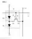
FIG. 1 is an equivalent circuit view of a semiconductor memory device according to the embodiment. The semiconductor memory device of the embodiment is an SRAM.
A memory cell 10 of the SRAM of the embodiment includes three elements: a first diode ND1; a second diode ND2; and a select transistor 12. The first diode ND1 and the second diode ND2 are formed by silicon nanowires. The diodes are silicon nanowire diodes exhibiting negative differential resistances. The first diode ND1 and the second diode ND2 are diodes having matched characteristics having equivalent function.
The first diode ND1 and the second diode ND2 are serially connected between power sources of two different potentials, which are Vdd and Vss. Vss has a lower potential than Vdd in the embodiment. To a connect point X between the first diode ND1 and the second diode ND2, a drain electrode 12a of the select transistor 12 is connected.
A source electrode 12b of the select transistor 12 is connected to a data line 14 and a gate electrode 12c is connected to an address line 16. In FIG. 1, only one memory cell 10 is shown, but actually, an SRAM is configured by arranging a plurality of memory cells 10 in an array.
FIG. 2 is a view showing current-voltage characteristic of a silicon nanowire diode. FIG. 2 shows a result calculated through a simulation of current-voltage characteristic of a device in which a silicon nanowire is sandwiched by electrodes. In the simulation, calculation is performed with a model considering phonon effect (lattice vibration effect). The silicon nanowires having columnar shape are used. A diameter (thickness) of the shape is 3 nm and a length of the shape is 10 nm. The silicon nanowires are of intrinsic silicon that contains little impurities.
The lateral axis shows the voltage applied between the electrodes, and the vertical axis shows the current flowing into the device. It can be seen that a negative differential resistance that causes the current to decrease as the voltage increases occurs in the current-voltage characteristic.
FIG. 3 is a view showing silicon nanowire diameter dependence of the current-voltage characteristic of a silicon nanowire diode. As is clear from FIG. 3, under the simulation conditions, negative differential resistance is hardly exhibited when the diameter (thickness) of the silicon nanowire is more than 8 nm and significantly exhibited when the diameter is 4 nm or less. Therefore, the thickness of the silicon nanowire is preferably 8 nm or less, and more preferably 4 nm or less.
It is considered that such negative differential resistance of a silicon nanowire diode is exhibited by phonon effect inherent to nanowires. When the wire becomes the size of nanometer, the lattice vibration energy (phonon energy) is quantized and becomes large. In the case of the energy difference between the carrier in wire and Fermi potential of electrode approaches to this phonon energy, the resonance of the carrier exchange between the channel and the electrode and of the carrier scattering by this phonon (quantized lattice vibration) occur. The current increases, because the carrier exchange rate of the wire and the electrode become large by this resonance. However, when the applied voltage increases so that the difference between the energy level of the carriers and the Fermi level of the electrode increases beyond the quantized energy, the current decreases.
Which means that the characteristic of the silicon nanowire diode is not caused by the tunneling effect of a tunneling device or the like. Therefore, it is considered that the characteristic is comparably stable against the process fluctuation such as fabrication fluctuation, impurity distribution fluctuation, and impurity concentration fluctuation.
FIG. 4 is an explanatory view of memory cell operation of the embodiment. The lateral axis of FIG. 4 shows the potential of the connect point X between the first diode ND1 and the second diode ND2 of FIG. 1 and the vertical axis shows the current flowing into the first diode ND1 and the second diode ND2. The current flowing into the first diode ND1 is shown by a solid line and the current flowing into the second diode ND2 is shown by a dashed line.
The memory cell becomes in a stable state at two potentials V1 and V2 of the connect point X both causing the same current I0 to flow from the current storage side at the connect point X. The memory cell 10 operates by defining one of the two stable potentials to be “1” and the other is defined to be “0”.
Upon write operation, a potential is applied to the address line 16 connected to the gate electrode 12c of the select transistor 12 to turn on the select transistor 12, thereby applying the voltage V1 or V2 to the data line 14. Accordingly, the potential between the source electrode 12b and the drain electrode 12a of the select transistor 12 connected to the data line 14 becomes zero and the potential of the connect point X becomes the applied potential V1 or V2. This state is maintained even when the select transistor 12 is turned off since the potential written into the memory cell 10 is in the stable state.
Upon read operation, a potential is applied to the address line 16 connected to the gate electrode 12c of the select transistor 12 to turn on the select transistor 12. Then, the potential V1 or V2 stored at the connect point X is output to the data line 14 connected to the source electrode 12b so that the potential written into the memory cell 10 can be read.
In this way, the memory cell 10 operates as a memory cell of an SRAM.
In the semiconductor memory device of the embodiment, the characteristic of the silicon nanowire diode mainly depends on the thickness of the silicon nanowires. Accordingly, if control of the thickness of the silicon nanowires is particularly kept, the characteristic can be significantly stable against other process fluctuation such as fabrication fluctuation, impurity concentration fluctuation, or impurity distribution fluctuation. Therefore, it is possible to provide a semiconductor memory device capable of stably operating even when an element is shrank or scaled-down. This means that it is possible to provide a semiconductor memory device capable of stably operating with high memory capacity.
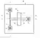
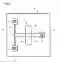
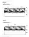
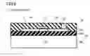
FIG. 5 is a schematic top view of the semiconductor memory device according to the embodiment. FIGS. 6 to 8 are respectively a section view taken along line A-A, a section view taken along line B-B, and a section view taken along line C-C of FIG. 5.
The semiconductor device of the embodiment is formed on an SOI (Silicon On Insulator) substrate 20. The SOI substrate includes: a silicon substrate 20a; an insulating layer 20b; and SOI layers 20c.
A silicon nanowire 21 of the first diode ND1 and a silicon nanowire 22 of the second first diode ND2 are both formed by the SOI layers 20c. The silicon nanowires 21 and 22 are non-doped intrinsic silicon or single conductivity type, which is n-type or p-type, silicon.
The width and height of the silicon nanowires 21 and 22 are 4 μm or less, for example. On the silicon nanowires 21 and 22, an interlayer film 50 is formed.
On the SOI layer 20c on one end of the silicon nanowire 21, a Vss contact electrode 31 is formed. On the other end of the silicon nanowire 21, the silicon nanowire 22 is formed through the SOI layer 20c serving as the connect point X. On the SOI layer 20c on a side of the silicon nanowire 22 opposite to the connect point X, a Vdd contact electrode 32 is formed.
The SOI layers 20c under the Vss contact electrode 31 and the Vdd contact electrode 32 may be doped with n-type or p-type impurities in order to decrease contact resistance. When the silicon nanowires 21 and 22 are doped, the silicon nanowires and the SOI layers 20c under the contact electrode are of the same conductivity type in order not to form p-n junction therebetween.
The drain electrode 12a, the source electrode 12b, and a channel region 12d of the select transistor 12 are formed in the SOI layer 20c. The drain electrode 12a and the source electrode 12b are formed by n-type impurity diffusion layers, for example. On the channel region 12d, the gate electrode 12c is formed on a gate insulating film. On the SOI layer 20c on the source electrode 12b side, a data line contact electrode 33 is formed.
The semiconductor memory device shown in FIGS. 5 to 8 can be formed by a process common with a select transistor of a planar MIS transistor by forming the silicon nanowires by the SOI layers. Therefore, a semiconductor memory device capable of stably operating even when an element is shrank or scaled-down can be realized through a process which can be well matched with processes of other elements and which is simple.
The thickness (or width) of the silicon nanowires is controlled by masking regions other than the silicon nanowires after the SOI layers 20c are patterned, for example, and then performing isotropic etching and oxidation of silicon, for example. In this way, SOI layers right after the patterning can be thinned and fined more so as to decrease the thickness and the width, whereby silicon nanowires having a desired thickness (or width) can be realized.
Second Embodiment
A semiconductor memory device of the embodiment is the same as that of the first embodiment except that nanowires are germanium nanowires instead of the silicon nanowires. Therefore, the contents overlapping with the first embodiment will not be repeated.
A germanium nanowire is a semiconductor of Group IV similarly to silicon and the crystal structure thereof is diamond structure also similarly to silicon. Accordingly, a germanium nanowire is considered to exhibit negative differential resistance due to phonon effect similarly to a silicon nanowire. Therefore, an effect similarly to the first embodiment can be expected using germanium nanowires.
While certain embodiments have been described, these embodiments have been presented by way of example only, and are not intended to limit the scope of the inventions. Indeed, the semiconductor memory device described herein may be embodied in a variety of other forms; furthermore, various omissions, substitutions and changes in the form of the devices and methods described herein may be made without departing from the spirit of the inventions. The accompanying claims and their equivalents are intended to cover such forms or modifications as would fall within the scope and spirit of the inventions.
For example, in the first embodiment, a case where the silicon nanowires are formed by the SOI layers is exemplified, but a memory cell may be structured by forming electrodes on silicon nanowires grown by vapor using CVD method or the like, for example.
For example, in the embodiments, a case where the select transistor is formed by a planar MIS transistor is exemplified, but the select transistor may be a nanowire transistor using a nanowire.
For example, in the embodiments, a case where the nanowire diodes are formed by lateral devices is exemplified, but the nanowire diodes may be formed by a vertical devices.
Claims
What is claimed is:1. A semiconductor memory device comprising:
first and second diodes serially connected between power sources of two different potentials, the diodes being formed by nanowires, and exhibiting negative differential resistances; and
a select transistor connected between the first diode and the second diode.
2. The device according to claim 1, wherein the nanowires are silicon nanowires.
3. The device according to claim 2, wherein a thickness of the silicon nanowires is 8 nm or less.
4. The device according to claim 2, wherein the silicon nanowires are formed by intrinsic silicon or single conductivity type silicon.
5. The device according to claim 2, wherein the silicon nanowires are formed in an SOI layer of an SOI substrate.
6. A semiconductor memory device comprising:
first and second diodes serially connected between power sources of two different potentials, the diodes being formed by nanowires, and exhibiting negative differential resistances;
a select transistor, a drain electrode of the select transistor being connected between the first diode and the second diode;
a data line being connected to a source electrode of the select transistor; and
an address line being connected to a gate electrode of the select transistor.
7. The device according to claim 6, wherein the nanowires are silicon nanowires.
8. The device according to claim 7, wherein a thickness of the silicon nanowires is 8 nm or less.
9. The device according to claim 7, wherein the silicon nanowires are formed by intrinsic silicon or single conductivity type silicon.
10. The device according to claim 7, wherein the silicon nanowires are formed in an SOI layer of an SOI substrate.
Images & Drawings included:


Sources:
- United States Patent and Trademark Office - verify current appl. status at the USPTO↗
Similar patent applications:
Recent applications in this class:
- » 20210188629 2021-06-24
Method of ono integration into logic CMOS flow - » 20200385266 2020-12-10
Quantum shift register structures - » 20200369517 2020-11-26
Amplitude, frequency, and phase modulated entangling gates for trapped-ion quantum computers - » 20200307995 2020-10-01
Machine Learning Processor Employing a Monolithically Integrated Memory System - » 20200109049 2020-04-09
Nanowire arrays for trace vapor preconcentration - » 20200079648 2020-03-12
Syndrome of degraded quantum redundancy coded states - » 20190337800 2019-11-07
Semiconductor arrangement with one or more semiconductor columns - » 20190194016 2019-06-27
QUANTUM COMPUTING ASSEMBLIES - » 20180237294 2018-08-23
Nanowire arrays for trace vapor preconcentration - » 20180002172 2018-01-04
Semiconductor arrangement with one or more semiconductor columns
Recent applications for this Assignee:
- » 20250294845 2025-09-18
SEMICONDUCTOR DEVICE - » 20250294830 2025-09-18
SEMICONDUCTOR DEVICE - » 20250294829 2025-09-18
SEMICONDUCTOR DEVICE - » 20250294786 2025-09-18
SEMICONDUCTOR DEVICE - » 20250294110 2025-09-18
CODE RECOGNITION METHOD, INSPECTION DEVICE, AND STORAGE MEDIUM - » 20250293867 2025-09-18
CONTROL DEVICE, QUANTUM KEY DISTRIBUTION SYSTEM, CONTROL METHOD, AND COMPUTER PROGRAM PRODUCT - » 20250293865 2025-09-18
QUANTUM KEY DISTRIBUTION SYSTEM, QUANTUM KEY DISTRIBUTION DEVICE, AND QUANTUM KEY DISTRIBUTION METHOD - » 20250293784 2025-09-18
AN OPTICAL TRANSMITTER, A QUANTUM COMMUNICATION SYSTEM AND A METHOD OF OPERATING AN OPTICAL TRANSMITTER - » 20250293414 2025-09-18
BATTERY - » 20250293316 2025-09-18
NONAQUEOUS ELECTROLYTE BATTERY AND BATTERY PACK