Power semiconductor module
US20110249407A1
2011-10-13
12/910,231
2010-10-22
✅ Patent granted
US 8,558,361 B2
2013-10-15
-
-
Michelle Mandala
Oblon, Spivak, McClelland, Maier & Neustadt, L.L.P.
2031-05-01
Abstract:
A power semiconductor module comprises: a heat dissipation plate; an insulating wiring board having an upper electrode and a lower electrode, the lower electrode joined to the heat dissipation plate via a first solder; a semiconductor chip joined to the upper electrode via a second solder; a first low-dielectric film coating sides of the lower electrode and the first solder; a second low-dielectric film coating sides of the semiconductor chip and the second solder; a case on the heat dissipation plate and surrounding the insulating wiring board and the semiconductor chip; and an insulator filled in the case and coating the insulating wiring board, the semiconductor chip, and the first and second low-dielectric films.
Assignee:
- MITSUBISHI ELECTRIC CORPORATION 16,560 🇯🇵 TOKYO, Japan
- Mitsubishi Electric Corporation 2,856 🇯🇵 Chiyoda-ku, Japan
Applicant:
Interested in similar patents?
Get notified when new applications in this technology area are published.
Classification:
H01L23/24 » CPC main
Details of semiconductor or other solid state devices; Fillings or auxiliary members in containers or encapsulations , e.g. centering rings; Fillings characterised by the material, its physical or chemical properties, or its arrangement within the complete device solid or gel at the normal operating temperature of the device
H01L23/053 » CPC further
Details of semiconductor or other solid state devices; Containers; Seals characterised by the shape of the container or parts, e.g. caps, walls the container being a hollow construction and having an insulating or insulated base as a mounting for the semiconductor body
H01L23/3121 » CPC further
Details of semiconductor or other solid state devices; Encapsulations, e.g. encapsulating layers, coatings, e.g. for protection characterised by the arrangement or shape the device being completely enclosed a substrate forming part of the encapsulation
H01L23/3185 » CPC further
Details of semiconductor or other solid state devices; Encapsulations, e.g. encapsulating layers, coatings, e.g. for protection characterised by the arrangement or shape; Partial encapsulation or coating the coating covering also the sidewalls of the semiconductor body
H01L23/60 » CPC further
Details of semiconductor or other solid state devices; Structural electrical arrangements for semiconductor devices not otherwise provided for, e.g. in combination with batteries Protection against electrostatic charges or discharges, e.g. Faraday shields
H01L24/29 » CPC further
Arrangements for connecting or disconnecting semiconductor or solid-state bodies; Methods or apparatus related thereto; Means for bonding being attached to, or being formed on, the surface to be connected, e.g. chip-to-package, die-attach, "first-level" interconnects; Manufacturing methods related thereto; Layer connectors, e.g. plate connectors, solder or adhesive layers; Manufacturing methods related thereto; Structure, shape, material or disposition of the layer connectors prior to the connecting process of an individual layer connector
H01L24/32 » CPC further
Arrangements for connecting or disconnecting semiconductor or solid-state bodies; Methods or apparatus related thereto; Means for bonding being attached to, or being formed on, the surface to be connected, e.g. chip-to-package, die-attach, "first-level" interconnects; Manufacturing methods related thereto; Layer connectors, e.g. plate connectors, solder or adhesive layers; Manufacturing methods related thereto; Structure, shape, material or disposition of the layer connectors after the connecting process of an individual layer connector
H01L24/49 » CPC further
Arrangements for connecting or disconnecting semiconductor or solid-state bodies; Methods or apparatus related thereto; Means for bonding being attached to, or being formed on, the surface to be connected, e.g. chip-to-package, die-attach, "first-level" interconnects; Manufacturing methods related thereto; Wire connectors; Manufacturing methods related thereto; Structure, shape, material or disposition of the wire connectors after the connecting process of a plurality of wire connectors
H01L25/072 » CPC further
Assemblies consisting of a plurality of individual semiconductor or other solid state devices ; Multistep manufacturing processes thereof all the devices being of a type provided for in the same subgroup of groups - , e.g. assemblies of rectifier diodes the devices not having separate containers the devices being of a type provided for in group the devices being arranged next to each other
H01L23/367 » CPC further
Details of semiconductor or other solid state devices; Arrangements for cooling, heating, ventilating or temperature compensation ; Temperature sensing arrangements; Selection of materials, or shaping, to facilitate cooling or heating, e.g. heatsinks Cooling facilitated by shape of device
H01L24/45 » CPC further
Arrangements for connecting or disconnecting semiconductor or solid-state bodies; Methods or apparatus related thereto; Means for bonding being attached to, or being formed on, the surface to be connected, e.g. chip-to-package, die-attach, "first-level" interconnects; Manufacturing methods related thereto; Wire connectors; Manufacturing methods related thereto; Structure, shape, material or disposition of the wire connectors prior to the connecting process of an individual wire connector
H01L24/48 » CPC further
Arrangements for connecting or disconnecting semiconductor or solid-state bodies; Methods or apparatus related thereto; Means for bonding being attached to, or being formed on, the surface to be connected, e.g. chip-to-package, die-attach, "first-level" interconnects; Manufacturing methods related thereto; Wire connectors; Manufacturing methods related thereto; Structure, shape, material or disposition of the wire connectors after the connecting process of an individual wire connector
H01L2224/49 » CPC further
Indexing scheme for arrangements for connecting or disconnecting semiconductor or solid-state bodies and methods related thereto as covered by; Means for bonding being attached to, or being formed on, the surface to be connected, e.g. chip-to-package, die-attach, "first-level" interconnects; Manufacturing methods related thereto; Wire connectors; Manufacturing methods related thereto; Structure, shape, material or disposition of the wire connectors after the connecting process of a plurality of wire connectors
H01L2224/83051 » CPC further
Indexing scheme for arrangements for connecting or disconnecting semiconductor or solid-state bodies and methods related thereto as covered by; Methods for connecting semiconductor or other solid state bodies using means for bonding being attached to, or being formed on, the surface to be connected using a layer connector; Pre-treatment of the layer connector or the bonding area Forming additional members, e.g. dam structures
H01L2224/83951 » CPC further
Indexing scheme for arrangements for connecting or disconnecting semiconductor or solid-state bodies and methods related thereto as covered by; Methods for connecting semiconductor or other solid state bodies using means for bonding being attached to, or being formed on, the surface to be connected using a layer connector; Post-treatment of the layer connector or bonding area Forming additional members, e.g. for reinforcing, fillet sealant
H01L2924/01006 » CPC further
Indexing scheme for arrangements or methods for connecting or disconnecting semiconductor or solid-state bodies as covered by; Chemical elements Carbon [C]
H01L2924/01013 » CPC further
Indexing scheme for arrangements or methods for connecting or disconnecting semiconductor or solid-state bodies as covered by; Chemical elements Aluminum [Al]
H01L2924/01014 » CPC further
Indexing scheme for arrangements or methods for connecting or disconnecting semiconductor or solid-state bodies as covered by; Chemical elements Silicon [Si]
H01L2924/01029 » CPC further
Indexing scheme for arrangements or methods for connecting or disconnecting semiconductor or solid-state bodies as covered by; Chemical elements Copper [Cu]
H01L2924/01033 » CPC further
Indexing scheme for arrangements or methods for connecting or disconnecting semiconductor or solid-state bodies as covered by; Chemical elements Arsenic [As]
H01L2924/13055 » CPC further
Indexing scheme for arrangements or methods for connecting or disconnecting semiconductor or solid-state bodies as covered by; Details of semiconductor or other solid state devices to be connected; Device type; Discrete devices, e.g. 3 terminal devices; Transistor; Bipolar Junction Transistor [BJT] Insulated gate bipolar transistor [IGBT]
H01L2924/16195 » CPC further
Indexing scheme for arrangements or methods for connecting or disconnecting semiconductor or solid-state bodies as covered by; Details of package parts other than the semiconductor or other solid state devices to be connected; Cap; Shape Flat cap [not enclosing an internal cavity]
H01L2924/00014 » CPC further
Indexing scheme for arrangements or methods for connecting or disconnecting semiconductor or solid-state bodies as covered by; Technical content checked by a classifier the subject-matter covered by the group, the symbol of which is combined with the symbol of this group, being disclosed without further technical details
H01L2224/73265 » CPC further
Indexing scheme for arrangements for connecting or disconnecting semiconductor or solid-state bodies and methods related thereto as covered by; Means for bonding being of different types provided for in two or more of groups; Location after the connecting process on different surfaces Layer and wire connectors
H01L2924/0665 » CPC further
Indexing scheme for arrangements or methods for connecting or disconnecting semiconductor or solid-state bodies as covered by; Polymers Epoxy resin
H01L2924/014 » CPC further
Indexing scheme for arrangements or methods for connecting or disconnecting semiconductor or solid-state bodies as covered by; Alloys Solder alloys
H01L2224/27013 » CPC further
Indexing scheme for arrangements for connecting or disconnecting semiconductor or solid-state bodies and methods related thereto as covered by; Means for bonding being attached to, or being formed on, the surface to be connected, e.g. chip-to-package, die-attach, "first-level" interconnects; Manufacturing methods related thereto; Layer connectors, e.g. plate connectors, solder or adhesive layers; Manufacturing methods related thereto; Manufacturing methods; Involving a permanent auxiliary member, i.e. a member which is left at least partly in the finished device, e.g. coating, dummy feature for holding or confining the layer connector, e.g. solder flow barrier
H01L2924/181 » CPC further
Indexing scheme for arrangements or methods for connecting or disconnecting semiconductor or solid-state bodies as covered by; Details of package parts other than the semiconductor or other solid state devices to be connected Encapsulation
H01L2924/07025 » CPC further
Indexing scheme for arrangements or methods for connecting or disconnecting semiconductor or solid-state bodies as covered by; Polymers; Polyamine or polyimide Polyimide
H01L2924/1305 » CPC further
Indexing scheme for arrangements or methods for connecting or disconnecting semiconductor or solid-state bodies as covered by; Details of semiconductor or other solid state devices to be connected; Device type; Discrete devices, e.g. 3 terminal devices; Transistor Bipolar Junction Transistor [BJT]
H01L2924/00 » CPC further
Indexing scheme for arrangements or methods for connecting or disconnecting semiconductor or solid-state bodies as covered by
H01L2924/00012 » CPC further
Indexing scheme for arrangements or methods for connecting or disconnecting semiconductor or solid-state bodies as covered by; Technical content checked by a classifier Relevant to the scope of the group, the symbol of which is combined with the symbol of this group
H01L23/34 IPC
Details of semiconductor or other solid state devices Arrangements for cooling, heating, ventilating or temperature compensation ; Temperature sensing arrangements
H05K7/20 IPC
Constructional details common to different types of electric apparatus Modifications to facilitate cooling, ventilating, or heating
H05K7/20 IPC
Constructional details common to different types of electric apparatus Modifications to facilitate cooling, ventilating, or heating
H01L23/495 IPC
Details of semiconductor or other solid state devices; Arrangements for conducting electric current to or from the solid state body in operation, e.g. leads, terminal arrangements ; Selection of materials therefor consisting of soldered constructions Lead-frames or other flat leads
Description
BACKGROUND OF THE INVENTION
1. Field of the Invention
The present invention relates to a power semiconductor module comprising a double-sided electrode type insulating wiring board, and in particular to a power semiconductor module capable of reducing insulation failure.
2. Background Art
In recent years, a power semiconductor module is used in a power converter for controlling electrical equipment such as motors. In the power semiconductor module, a double-sided electrode type insulating wiring board joined on a heat dissipation plate with a solder, and semiconductor chips are joined on the insulating wiring board with the solder. A case capsules the insulating wiring board and semiconductor chips, and the case is filled with silicone gel (for example, refer to Japanese Patent Laid-Open No. 2002-76190).
SUMMARY OF THE INVENTION
Bubbles may be formed from a solder into the silicone gel in the circumferential part of the module due to temperature change when applying current. By these bubbles, insulation failure may occur. Particularly, bubbles in the circumferential part of the double-sided electrode type insulating wiring board joined on the heat dissipation plate directly cause insulation failure.
In view of the above-described problems, an object of the present invention is to provide a power semiconductor module capable of reducing insulation failure.
According to the present invention, a power semiconductor module comprises: a heat dissipation plate; an insulating wiring board having an upper electrode and a lower electrode, the lower electrode joined to the heat dissipation plate via a first solder; a semiconductor chip joined to the upper electrode via a second solder; a first low-dielectric film coating sides of the lower electrode and the first solder; a second low-dielectric film coating sides of the semiconductor chip and the second solder; a case on the heat dissipation plate and surrounding the insulating wiring board and the semiconductor chip; and an insulator filled in the case and coating the insulating wiring board, the semiconductor chip, and the first and second low-dielectric films.
The present invention makes it possible to reduce insulation failure.
Other and further objects, features and advantages of the invention will appear more fully from the following description.
BRIEF DESCRIPTION OF THE DRAWINGS
FIG. 1 is a sectional view showing a power semiconductor module according to the first embodiment.
FIG. 2 is a top view showing a power semiconductor module according to the first embodiment.
FIG. 3 is an equivalent circuit of one circuit block in the power semiconductor module shown in FIG. 2.
FIG. 4 is an enlarged sectional view showing a power semiconductor module according to the first embodiment.
FIG. 5 is an enlarged sectional view showing a power semiconductor module according to the second embodiment.
FIG. 6 is an enlarged sectional view showing a power semiconductor module according to the third embodiment.
FIG. 7 is an enlarged sectional view showing a power semiconductor module according to the fourth embodiment.
FIG. 8 is an enlarged sectional view showing a power semiconductor module according to the fifth embodiment.
DETAILED DESCRIPTION OF THE PREFERRED EMBODIMENTS
A power semiconductor module according to the embodiments of the present invention will be described with reference to the drawings. The same components will be denoted by the same symbols, and the repeated description thereof may be omitted.
First Embodiment
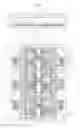
FIG. 1 is a sectional view showing a power semiconductor module according to the first embodiment, and FIG. 2 is a top view thereof. The power semiconductor module incorporates circuit blocks configured to obtain high breakdown voltage and large current characteristics by connecting a plurality of insulating-gate bipolar transistors (IGBT) in parallel and providing common collector terminals, emitter terminals, and gate terminals. FIG. 3 is an equivalent circuit of one circuit block in the power semiconductor module shown in FIG. 2.
On a heat dissipation plate 1, drive circuit wiring boards 2, power semiconductor circuit wiring boards 3, and relay circuit wiring boards 4 are installed. These circuit wiring boards are insulating wiring boards such as ceramics having conductive patterns of cupper, aluminum, or the like on both surfaces. On the power semiconductor circuit wiring boards 3, IGBTs 5 and free wheel diodes 6 are joined. Chip resistors 7 are joined onto the drive circuit wiring boards 2.
The emitters of the IGBTs 5 and the anodes of the free wheel diodes 6 are connected to the conductive patterns of the relay circuit wiring boards by Al wires 8. The gates of the IGBTs 5 are connected to the conductive patterns of the drive circuit wiring board 2 by Al wires 8. The collectors of the IGBTs 5 and the cathodes of the free wheel diodes 6 are mutually connected via the conductive patterns of the power semiconductor circuit wiring boards 3.
A plastic case 9 is provided on the heat dissipation plate 1 so as to surround the drive circuit wiring board 2, the power semiconductor circuit wiring boards 3, and the relay circuit wiring boards 4, and a cover 10 is placed on the upper portion of the case 9. The case 9 is filled with silicone gel 11 for maintaining air tightness and insulation. Each circuit wiring board is equipped with an electrode terminal joining region 12. To the electrode terminal joining region 12, an electrode terminal (not shown) for realizing electrical connection to the exterior is installed. Here, although the power semiconductor circuit wiring board 3 and the relay circuit wiring board 4 are separately installed on different insulating wiring board, the both may be provided on different conductive pattern forming regions of one insulating wiring board.
FIG. 4 is an enlarged sectional view showing a power semiconductor module according to the first embodiment. An insulating wiring board 13 has an upper electrode 14 and a lower electrode 15. The lower electrode 15 of the insulating wiring board 13 is joined to the heat dissipation plate 1 via a solder 16. A semiconductor chip 18 made of Si is joined on the upper electrode 14 of the insulating wiring board 13 via solder 17. An Al wire 8 is bonded to the semiconductor chip 18. The insulating wiring board 13 corresponds to the power semiconductor circuit wiring board 3 shown in FIGS. 1 to 3, and the semiconductor chip 18 corresponds to the IGBT 5 or the free wheel diode 6 shown in FIGS. 1 to 3.
A low-dielectric film 19 coats sides of the lower electrode 15 and the solder 16. A low-dielectric film 20 coats sides of the semiconductor chip 18 and the solder 17. The low-dielectric films 19 and 20 are composed of one of silicone rubber, polyimide, and epoxy resin. In particular, when silicone rubber is used as the low-dielectric films 19 and 20, assembly is facilitated. When polyimide is used, heat resistance is improved. When epoxy resin is used, heat cycling characteristics are improved. A silicone gel 11 (flexible insulator) filled in the case 9 coats the insulating wiring board 13, the semiconductor chip 18, and the low-dielectric films 19 and 20.
As described above, in the present embodiment, the low-dielectric film 19 coats the sides of the solder 16 and the lower electrode 15, and the low-dielectric film 20 coats the sides of the solder 17 and the semiconductor chip 18. Thereby, the generation of bubbles from the solder 17 can be suppressed. Therefore, the insulation failure can be reduced, and the life elongation of the products becomes feasible.
Second Embodiment
FIG. 5 is an enlarged sectional view showing a power semiconductor module according to the second embodiment. The low-dielectric film 19 coats the entire upper surface of the heat dissipation plate 1 in the lower side than the insulating wiring board 13. Other configurations are identical to the configurations of the first embodiment. Thereby, the generation of bubbles from the solder 16 can be more reliably suppressed than the first embodiment.
Third Embodiment
FIG. 6 is an enlarged sectional view showing a power semiconductor module according to the third embodiment. Although the low-dielectric film 19 is not formed, the insulating wiring board 13 has further a convex portion 21 protruded downward from the peripheral portion of the lower surface. Other configurations are identical to the configurations of the first embodiment. Thereby, bubbles generated from the solder 16 are stopped on the lower surface side of the insulating wiring board 13 by the convex portion 21. Therefore, insulation failure can be reduced.
Fourth Embodiment
FIG. 7 is an enlarged sectional view showing a power semiconductor module according to the fourth embodiment. A partition 22 is formed on the internal wall of the case 9. The partition 22 is placed between the joining portion 23 of the heat dissipation plate 1 with case 9 and the upper surface of the insulating wiring board 13. Other configurations are identical to the configurations of the first embodiment.
Bubbles generated from the joining portion 23 are stopped in the case 9 side by the partition 22, and do not move to the upper surface of the insulating wiring board 13. Therefore, insulation failure can be further reduced.
The distance from the joining portion 23 to the upper surface of the insulating wiring board 13 is longer than the distance from solders 16 and 17 to the upper surface of the insulating wiring board 13. Therefore, the possibility that the bubbles cause insulation failure is low. However, the present embodiment is effective when further high reliability is required.
The configuration of the fourth embodiment can be applied not only to the first embodiment, but also to any of second and third embodiments.
Fifth Embodiment
FIG. 8 is an enlarged sectional view showing a power semiconductor module according to the fifth embodiment. In the first to fourth embodiment, the silicone gel 11 coats all the Al wires 8. Whereas in the fifth embodiment, the height of the silicone gel 11 is limited to be about several millimeters from the upper surface of the semiconductor chip 18. Thereby, a part of the Al wires 8 is exposed from the silicone gel 11. Other configurations are identical to the configurations of the first embodiment.
Even if bubbles are generated from solders 16 and 17 due to defective forming of low-dielectric films 19 and 20, the bubbles easily reach the upper surface of the silicone gel 11, and released into the air. Therefore, insulation failure can be further reduced.
The configuration of the fifth embodiment can be applied not only to the first embodiment, but also to any of second to fourth embodiments.
Obviously many modifications and variations of the present invention are possible in the light of the above teachings. It is therefore to be understood that within the scope of the appended claims the invention may be practiced otherwise than as specifically described.
The entire disclosure of a Japanese Patent Application No. 2010-091291, filed on Apr. 12, 2010 including specification, claims, drawings and summary, on which the Convention priority of the present application is based, are incorporated herein by reference in its entirety.
Claims
What is claimed is:1. A power semiconductor module comprising:
a heat dissipation plate;
an insulating wiring board having an upper electrode and a lower electrode, the lower electrode joined to the heat dissipation plate via a first solder;
a semiconductor chip joined to the upper electrode via a second solder;
a first low-dielectric film coating sides of the lower electrode and the first solder;
a second low-dielectric film coating sides of the semiconductor chip and the second solder;
a case on the heat dissipation plate and surrounding the insulating wiring board and the semiconductor chip; and
an insulator filled in the case and coating the insulating wiring board, the semiconductor chip, and the first and second low-dielectric films.
2. The power semiconductor module according to claim 1, wherein the first and second low-dielectric films are composed of one of silicone rubber, polyimide, and epoxy resin.
3. The power semiconductor module according to claim 1, wherein the first low-dielectric film coats an entire upper surface of the heat dissipation plate in a lower side than the insulating wiring board.
4. The power semiconductor module according to claim 1, wherein the insulating wiring board has a convex portion protruded downward from a peripheral portion of a lower surface of the insulating wiring board.
5. The power semiconductor module according to claim 1, further comprising a partition placed between a joining portion of the heat dissipation plate with the case and an upper surface of the insulating wiring board.
6. The power semiconductor module according to claim 1, further comprising a wire bonded to the semiconductor chip, wherein a part of the wire is exposed from the insulator.
Images & Drawings included:


Sources:
- United States Patent and Trademark Office - verify current appl. status at the USPTO↗
Similar patent applications:
- » 20220139797
Semiconductor module, power semiconductor module, and power electronic equipment using the semiconductor module or the power semiconductor module - » 20100252922
Power semiconductor module, power semiconductor module assembly and method for fabricating a power semiconductor module assembly - » 20240260168
CIRCUIT BOARD FOR A POWER SEMICONDUCTOR MODULE, POWER SEMICONDUCTOR MODULE, AND METHOD FOR PRODUCING A CIRCUIT BOARD AND A POWER SEMICONDUCTOR MODULE - » 20230155479
Power semiconductor module, power electronic assembly including one or more power semiconductor modules, and power conversion control circuit for a power semiconductor module - » 20140225245
Power semiconductor module and power semiconductor module assembly with multiple power semiconductor modules - » 20250259909
A HEAT DISSIPATION SUBSTRATE FOR A POWER SEMICONDUCTOR MODULE, A POWER SEMICONDUCTOR MODULE INCLUDING THE SAME AND A POWER CONVERTER INCLUDING THE SAME, AND MANUFACTURING METHOD OF THE HEAT DISSIPATION SUBSTRATE FOR A POWER SEMICONDUCTOR MODULE - » 20250259908
HEAT DISSIPATION SUBSTRATE FOR A POWER SEMICONDUCTOR MODULE, A POWER SEMICONDUCTOR MODULE INCLUDING THE SAME AND A POWER CONVERTER INCLUDING THE SAME, AND MANUFACTURING METHOD OF THE HEAT DISSIPATION SUBSTRATE FOR A POWER SEMICONDUCTOR MODULE - » 20250118636
HEAT DISSIPATION SUBSTRATE FOR A POWER SEMICONDUCTOR MODULE, A POWER SEMICONDUCTOR MODULE INCLUDING THE HEAT DISSIPATION SUBSTRATE, AND A POWER CONVERTER INCLUDING THE POWER SEMICONDUCTOR MODULE - » 20250118680
HEAT DISSIPATION SUBSTRATE FOR A POWER SEMICONDUCTOR MODULE, A POWER SEMICONDUCTOR MODULE INCLUDING THE HEAT DISSIPATION SUBSTRATE, AND A POWER CONVERTER INCLUDING THE POWER SEMICONDUCTOR MODULE - » 20230170287
POWER SEMICONDUCTOR MODULE, METHOD FOR ASSEMBLING A POWER SEMICONDUCTOR MODULE AND HOUSING FOR A POWER SEMICONDUCTOR MODULE
Recent applications in this class:
- » 20250279324 2025-09-04
PACKAGE WITH CARRIER HAVING COMPONENT ACCOMMODATION VOLUME ON ONE SIDE AND REPELLING STRUCTURE ON OTHER SIDE - » 20250273523 2025-08-28
GEL MATERIAL-FILLED POWER MODULE WITH A CIRCUIT CARRIER - » 20250239498 2025-07-24
SEMICONDUCTOR DEVICE AND MANUFACTURING METHOD THEREOF - » 20250233032 2025-07-17
DOUBLE-SIDED COOLING SEMICONDUCTOR DEVICE - » 20250226275 2025-07-10
COMPONENT-EMBEDDED STRUCTURE FOR WARPAGE SUPPRESSION - » 20250218881 2025-07-03
LIQUID-BASED METHOD FOR EMBEDDING COMPONENTS IN THICK SUBSTRATES - » 20250210429 2025-06-26
INTEGRATED CIRCUIT PACKAGES WITH STIFFENERS CONTAINING SEMICONDUCTOR DIES AND ASSOCIATED METHODS - » 20250210428 2025-06-26
STIFFENER ASSEMBLY - » 20250201643 2025-06-19
STACKED IC PACKAGE - » 20250167057 2025-05-22
Assemblage module 3D
Recent applications for this Assignee:
- » 20250294680 2025-09-18
POWER MODULE - » 20250293740 2025-09-18
WIRELESS COMMUNICATION SYSTEM - » 20250293196 2025-09-18
SEMICONDUCTOR DEVICE AND MANUFACTURING METHOD THEREOF - » 20250291113 2025-09-18
OPTICAL TERMINATOR, OPTICAL WAVELENGTH FILTER, AND EXTERNAL CAVITY LASER LIGHT SOURCE - » 20250290867 2025-09-18
SEMICONDUCTOR INSPECTION APPARATUS AND METHOD OF MANUFACTURING SEMICONDUCTOR DEVICE - » 20250290765 2025-09-18
INFORMATION PROCESSING DEVICE, INFORMATION PROCESSING METHOD, AND IMAGE PROJECTING SYSTEM - » 20250289592 2025-09-18
SPACE SITUATIONAL AWARENESS BUSINESS DEVICE AND SPACE TRAFFIC BUSINESS DEVICE - » 20250287683 2025-09-11
SEMICONDUCTOR DEVICE - » 20250287624 2025-09-11
POWER SEMICONDUCTOR DEVICE - » 20250287098 2025-09-11
DETECTION DEVICE, CAMERA SYSTEM, DETECTION METHOD, AND STORAGE MEDIUM STORING DETECTION PROGRAM