Integrated circuit device having through via and method for preparing the same
US20120126394A1
2012-05-24
12/949,058
2010-11-18
✅ Patent granted
US 8,421,193 B2
2013-04-16
-
-
Michael Jung
Novak Druce Connolly Bove + Quigg LLP
2031-06-03
Abstract:
An integrated circuit device includes a bottom wafer, at least one stacking wafer positioned on the bottom wafer, and at least one conductive via penetrating through the stacking wafer and into the bottom wafer in a substantially linear manner, wherein the bottom wafer and the stacking wafer are bonded by an intervening adhesive layer, and no bump pad is positioned between the bottom wafer and the stacking wafer. A method for preparing an integrated circuit device includes the steps of forming a bottom wafer, forming at least one stacking wafer, bonding the at least one stacking wafer to the bottom wafer by an intervening adhesive layer, and forming at least one conductive via penetrating through the stacking wafer and into the bottom wafer in a substantially linear manner, wherein no bump pad is positioned between the bottom wafer and the stacking wafer.
Assignee:
- NANYA TECHNOLOGY CORPORATION 34 🇹🇼 Kueishan, Taiwan
- Nanya Technology Corporation 7 🇹🇼 Kueishan, Tao-Yuan Hsien,, Taiwan
Applicant:
Interested in similar patents?
Get notified when new applications in this technology area are published.
Classification:
H01L29/40 IPC
Semiconductor devices adapted for rectifying, amplifying, oscillating or switching, or capacitors or resistors with at least one potential-jump barrier or surface barrier, e.g. PN junction depletion layer or carrier concentration layer; Details of semiconductor bodies or of electrodes thereof; Multistep manufacturing processes therefor Electrodes ; Multistep manufacturing processes therefor
H01L23/48 IPC
Details of semiconductor or other solid state devices Arrangements for conducting electric current to or from the solid state body in operation, e.g. leads, terminal arrangements ; Selection of materials therefor
H01L23/52 IPC
Details of semiconductor or other solid state devices Arrangements for conducting electric current within the device in operation from one component to another, i.e. interconnections, e.g. wires, lead frames
H01L21/30 IPC
Processes or apparatus adapted for the manufacture or treatment of semiconductor or solid state devices or of parts thereof; Manufacture or treatment of semiconductor devices or of parts thereof the devices having at least one potential-jump barrier or surface barrier, e.g. PN junction, depletion layer or carrier concentration layer the devices having semiconductor bodies comprising elements of Group IV of the Periodic System or AB compounds with or without impurities, e.g. doping materials Treatment of semiconductor bodies using processes or apparatus not provided for in groups -
H01L21/46 IPC
Processes or apparatus adapted for the manufacture or treatment of semiconductor or solid state devices or of parts thereof; Manufacture or treatment of semiconductor devices or of parts thereof the devices having at least one potential-jump barrier or surface barrier, e.g. PN junction, depletion layer or carrier concentration layer the devices having semiconductor bodies not provided for in groups, , , and with or without impurities, e.g. doping materials Treatment of semiconductor bodies using processes or apparatus not provided for in groups
H01L21/4763 IPC
Processes or apparatus adapted for the manufacture or treatment of semiconductor or solid state devices or of parts thereof; Manufacture or treatment of semiconductor devices or of parts thereof the devices having at least one potential-jump barrier or surface barrier, e.g. PN junction, depletion layer or carrier concentration layer the devices having semiconductor bodies not provided for in groups, , , and with or without impurities, e.g. doping materials; Treatment of semiconductor bodies using processes or apparatus not provided for in groups to change their surface-physical characteristics or shape, e.g. etching, polishing, cutting Deposition of non-insulating, e.g. conductive -, resistive -, layers on insulating layers; After-treatment of these layers
H01L21/44 IPC
Processes or apparatus adapted for the manufacture or treatment of semiconductor or solid state devices or of parts thereof; Manufacture or treatment of semiconductor devices or of parts thereof the devices having at least one potential-jump barrier or surface barrier, e.g. PN junction, depletion layer or carrier concentration layer the devices having semiconductor bodies not provided for in groups, , , and with or without impurities, e.g. doping materials Manufacture of electrodes on semiconductor bodies using processes or apparatus not provided for in groups -
H01L2224/94 » CPC further
Indexing scheme for arrangements for connecting or disconnecting semiconductor or solid-state bodies and methods related thereto as covered by; Batch processes at wafer-level, i.e. with connecting carried out on a wafer comprising a plurality of undiced individual devices
H01L25/0657 » CPC main
Assemblies consisting of a plurality of individual semiconductor or other solid state devices ; Multistep manufacturing processes thereof all the devices being of a type provided for in the same subgroup of groups - , e.g. assemblies of rectifier diodes the devices not having separate containers the devices being of a type provided for in group Stacked arrangements of devices
H01L21/6835 » CPC further
Processes or apparatus adapted for the manufacture or treatment of semiconductor or solid state devices or of parts thereof; Apparatus specially adapted for handling semiconductor or electric solid state devices during manufacture or treatment thereof; Apparatus specially adapted for handling wafers during manufacture or treatment of semiconductor or electric solid state devices or components ; Apparatus not specifically provided for elsewhere for supporting or gripping using temporarily an auxiliary support
H01L21/76224 » CPC further
Processes or apparatus adapted for the manufacture or treatment of semiconductor or solid state devices or of parts thereof; Manufacture or treatment of devices consisting of a plurality of solid state components formed in or on a common substrate or of parts thereof; Manufacture of integrated circuit devices or of parts thereof; Manufacture of specific parts of devices defined in group; Making of isolation regions between components; Dielectric regions, e.g. EPIC dielectric isolation, LOCOS; Trench refilling techniques, SOI technology, use of channel stoppers using trench refilling with dielectric materials
H01L21/76898 » CPC further
Processes or apparatus adapted for the manufacture or treatment of semiconductor or solid state devices or of parts thereof; Manufacture or treatment of devices consisting of a plurality of solid state components formed in or on a common substrate or of parts thereof; Manufacture of integrated circuit devices or of parts thereof; Manufacture of specific parts of devices defined in group; Applying interconnections to be used for carrying current between separate components within a device comprising conductors and dielectrics formed through a semiconductor substrate
H01L23/481 » CPC further
Details of semiconductor or other solid state devices; Arrangements for conducting electric current to or from the solid state body in operation, e.g. leads, terminal arrangements ; Selection of materials therefor Internal lead connections, e.g. via connections, feedthrough structures
H01L24/32 » CPC further
Arrangements for connecting or disconnecting semiconductor or solid-state bodies; Methods or apparatus related thereto; Means for bonding being attached to, or being formed on, the surface to be connected, e.g. chip-to-package, die-attach, "first-level" interconnects; Manufacturing methods related thereto; Layer connectors, e.g. plate connectors, solder or adhesive layers; Manufacturing methods related thereto; Structure, shape, material or disposition of the layer connectors after the connecting process of an individual layer connector
H01L24/92 » CPC further
Arrangements for connecting or disconnecting semiconductor or solid-state bodies; Methods or apparatus related thereto; Methods for connecting semiconductor or solid state bodies including different methods provided for in two or more of groups - Specific sequence of method steps
H01L24/94 » CPC further
Arrangements for connecting or disconnecting semiconductor or solid-state bodies; Methods or apparatus related thereto; Batch processes at wafer-level, i.e. with connecting carried out on a wafer comprising a plurality of undiced individual devices
H01L25/50 » CPC further
Assemblies consisting of a plurality of individual semiconductor or other solid state devices ; Multistep manufacturing processes thereof Multistep manufacturing processes of assemblies consisting of devices, each device being of a type provided for in group or
H01L24/29 » CPC further
Arrangements for connecting or disconnecting semiconductor or solid-state bodies; Methods or apparatus related thereto; Means for bonding being attached to, or being formed on, the surface to be connected, e.g. chip-to-package, die-attach, "first-level" interconnects; Manufacturing methods related thereto; Layer connectors, e.g. plate connectors, solder or adhesive layers; Manufacturing methods related thereto; Structure, shape, material or disposition of the layer connectors prior to the connecting process of an individual layer connector
H01L2221/68327 » CPC further
Processes or apparatus adapted for the manufacture or treatment of semiconductor or solid state devices or of parts thereof covered by; Apparatus for handling semiconductor or electric solid state devices during manufacture or treatment thereof; Apparatus for handling wafers during manufacture or treatment of semiconductor or electric solid state devices or components; Apparatus not specifically provided for elsewhere for supporting or gripping using temporarily an auxiliary support used during dicing or grinding
H01L2221/6834 » CPC further
Processes or apparatus adapted for the manufacture or treatment of semiconductor or solid state devices or of parts thereof covered by; Apparatus for handling semiconductor or electric solid state devices during manufacture or treatment thereof; Apparatus for handling wafers during manufacture or treatment of semiconductor or electric solid state devices or components; Apparatus not specifically provided for elsewhere for supporting or gripping using temporarily an auxiliary support used to protect an active side of a device or wafer
H01L2224/9202 » CPC further
Indexing scheme for arrangements for connecting or disconnecting semiconductor or solid-state bodies and methods related thereto as covered by; Methods for connecting semiconductor or solid state bodies including different methods provided for in two or more of groups - ; Specific sequence of method steps Forming additional connectors after the connecting process
H01L2224/92144 » CPC further
Indexing scheme for arrangements for connecting or disconnecting semiconductor or solid-state bodies and methods related thereto as covered by; Methods for connecting semiconductor or solid state bodies including different methods provided for in two or more of groups - ; Specific sequence of method steps; Connecting a surface with connectors of different types; Sequential connecting processes the first connecting process involving a layer connector the second connecting process involving a build-up interconnect
H01L2225/06541 » CPC further
Details relating to assemblies covered by the group but not provided for in its subgroups; All the devices being of a type provided for in the same subgroup of groups - the devices not having separate containers the devices being of a type provided for in group; Stacked arrangements of devices Conductive via connections through the device, e.g. vertical interconnects, through silicon via [TSV]
H01L2924/01029 » CPC further
Indexing scheme for arrangements or methods for connecting or disconnecting semiconductor or solid-state bodies as covered by; Chemical elements Copper [Cu]
H01L2924/01033 » CPC further
Indexing scheme for arrangements or methods for connecting or disconnecting semiconductor or solid-state bodies as covered by; Chemical elements Arsenic [As]
H01L2924/01074 » CPC further
Indexing scheme for arrangements or methods for connecting or disconnecting semiconductor or solid-state bodies as covered by; Chemical elements Tungsten [W]
H01L2924/00014 » CPC further
Indexing scheme for arrangements or methods for connecting or disconnecting semiconductor or solid-state bodies as covered by; Technical content checked by a classifier the subject-matter covered by the group, the symbol of which is combined with the symbol of this group, being disclosed without further technical details
H01L2924/014 » CPC further
Indexing scheme for arrangements or methods for connecting or disconnecting semiconductor or solid-state bodies as covered by; Alloys Solder alloys
H01L2224/83 » CPC further
Indexing scheme for arrangements for connecting or disconnecting semiconductor or solid-state bodies and methods related thereto as covered by; Methods for connecting semiconductor or other solid state bodies using means for bonding being attached to, or being formed on, the surface to be connected using a layer connector
H01L2924/14 » CPC further
Indexing scheme for arrangements or methods for connecting or disconnecting semiconductor or solid-state bodies as covered by; Details of semiconductor or other solid state devices to be connected; Device type Integrated circuits
H01L2924/00 » CPC further
Indexing scheme for arrangements or methods for connecting or disconnecting semiconductor or solid-state bodies as covered by
Description
BACKGROUND OF THE INVENTION
The present invention relates to an integrated circuit device having stacking wafers with through silicon vias and a method for preparing the same. More particularly, the present invention relates to an integrated circuit device and method for preparing the same by bonding wafers before the formation of the through silicon via.
Packaging technology for integrated circuit structures has been continuously developed to meet the demand for miniaturization and mounting reliability. Recently, as the miniaturization and high functionality of electric and electronic products are required, various techniques have been disclosed in the art.
By using a stack of at least two chips, i.e., the so-called 3D package, in the case of a memory device for example, it is possible to produce a product having a memory capacity which is twice as large as that obtainable through semiconductor integration processes. Also, a stack package provides advantages not only of an increase in memory capacity but also in regards to mounting density and mounting area utilization efficiency. Due to such advantages, research and development of stack package technology has accelerated.
As an example of a stack package, a through-silicon via (TSV) has been disclosed in the art. The stack package using a TSV has a structure in which the TSV is disposed in a chip so that chips are physically and electrically connected with each other through the TSV. Generally, a TSV is formed by etching a vertical via through a substrate and filling the via with a conductive material, such as copper. To increase the transmission speed and for high-density fabrication, the thickness of a semiconductor wafer comprising multiple integrated circuit structures each having the TSV should be reduced.
U.S. Pat. No. 7,683,459 discloses a hybrid bonding method for through silicon via based wafer stacking, in which patterned adhesive layers are provided to join together adjacent wafers in the stack, while solder bonding is used to electrically connect the lower end of the via in the upper wafer to the bump pad on the upper end of the via in the lower wafer. However, the formation of the bump pad on the upper end of the via requires seeding, electroplating, photolithography and etching processes; therefore, the formation of the bump pad on the upper end of the via is very complicated and expensive.
SUMMARY OF THE INVENTION
An aspect of the present invention is to provide an integrated circuit device and method for preparing the same by bonding wafers prior to the formation of the through silicon via such that no bump pad is positioned between the stacking wafer and the bottom wafer; therefore, the issues of complicated processing and high cost can be resolved.
One aspect of the present invention discloses an integrated circuit device comprising a bottom wafer, at least one stacking wafer positioned on the bottom wafer, and at least one conductive via penetrating through the stacking wafer and into the bottom wafer in a substantially linear manner, wherein the bottom wafer and the stacking wafer are bonded by an intervening adhesive layer, and no bump pad is positioned between the bottom wafer and the stacking wafer.
Another aspect of the present invention discloses a method for preparing an integrated circuit device comprising the steps of forming a bottom wafer, forming at least one stacking wafer, bonding the at least one stacking wafer to the bottom wafer by an intervening adhesive layer, and forming at least one conductive via penetrating through the stacking wafer and into the bottom wafer in a substantially linear manner, wherein no bump pad is positioned between the bottom wafer and the stacking wafer.
Compared to the technique disclosed in U.S. Pat. No. 7,683,459 forming one bump pad for each wafer, the embodiment of the present invention forms the integrated circuit device by bonding wafers prior to the formation of the through silicon via that penetrates through the stacking wafer and not through the bottom wafer. Consequently, the embodiment of the present invention does not need to form the bump pad between the stacking wafer and the bottom wafer; therefore, the issues of complicated processing and high cost can be resolved.
The foregoing has outlined rather broadly the features and technical advantages of the present invention in order that the detailed description of the invention that follows may be better understood. Additional features and advantages of the invention will be described hereinafter, and form the subject of the claims of the invention. It should be appreciated by those skilled in the art that the conception and specific embodiment disclosed may be readily utilized as a basis for modifying or designing other structures or processes for carrying out the same purposes as those of the present invention. It should also be realized by those skilled in the art that such equivalent constructions do not depart from the spirit and scope of the invention as set forth in the appended claims.
BRIEF DESCRIPTION OF THE DRAWINGS
The accompanying drawings, which are incorporated in and constitute a part of this specification, illustrate embodiments of the disclosure and, together with the description, serve to explain the principles of the invention.
FIGS. 1 through 12 are cross-sectional views illustrating a method for forming an integrated circuit device in accordance with one embodiment of the present invention.
DETAILED DESCRIPTION OF THE INVENTION
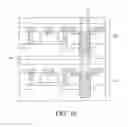
FIG. 1 to FIG. 12 are cross-sectional views illustrating a method for forming an integrated circuit device 100 in accordance with one embodiment of the present invention. Referring to FIG. 1, fabrication processes are performed to form an active element 13 such as a transistor in a silicon wafer 11, with a dielectric layer 15 covering the active element 13 and a shallow trench isolation 17 next to the active element 13 in the wafer 11. Subsequently, an etching process is performed to form a depression 19 in the shallow trench isolation 17, as shown in FIG. 2. In one embodiment of the present invention, the depression 19 penetrates through the shallow trench isolation 17.
Referring to FIG. 3, the depression 19 is filled with dielectric material by deposition process to form a dielectric block 21, and photolithographic and etching processes are then performed to remove a portion of the dielectric block 21 and the dielectric layer 15 to form at least one concavity 23. Referring to FIG. 4, photolithographic and etching processes are performed to remove a portion of the dielectric layer 15 to form at least one contact hole 25, which exposes at least one terminal of the active element 13, as shown in FIG. 4.
Referring to FIG. 5, a deposition process is performed to form a contact plug 27 by filling the contact hole 25 and an interconnect 29 by filling the concavity 23 with the same conductive material such as tungsten. Subsequently, a conductive layer 31 is formed by deposition process to electrically connect the interconnect 29 to the active element 13 through the contact plug 27, as shown in FIG. 6. In one embodiment of the present invention, the interconnect 29 and the conductive layer 31 form a connecting structure 30.
Referring to FIG. 7, a dielectric layer 33 is formed by deposition process to cover the conductive layer 31 and a passivation layer 35 is then formed by deposition process to cover the dielectric layer 33 to form a bottom wafer 10A. The fabrication processes shown in FIG. 1 to FIG. 6 are performed again on another wafer 11, a carrier 39 is adhered to the top side of the wafer 11 via an adhesive 37, and a thinning process such as the backside grinding process or CMP process is then performed to remove a portion of the wafer 11 from the bottom side of the wafer 11 to form a stacking wafer 10B, as shown in FIG. 8.
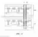
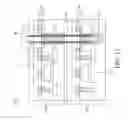
Referring to FIG. 9, the stacking wafer 10B is bonded to the bottom wafer 10A by an intervening adhesive layer 41 without forming a bump pad between the bottom wafer 10A and the stacking wafer 10B. In one embodiment of the present invention, the intervening adhesive layer 41 is the only layer between the bottom wafer 10A and the stacking wafer 10B, i.e., the stacking wafer 10B is bonded to the bottom wafer 11A without using solder. Subsequently, the carrier 39 and the adhesive 37 are removed from the top side of the stacking wafer 10B, and a dry etching process using fluorine-containing etching gas is then performed to form at least one via hole 43 penetrating through the stacking wafer 10B and into the bottom wafer 10A in a substantially linear manner, as shown in FIG. 10. In one embodiment of the present invention, the at least one via hole 43 does not penetrate through the bottom wafer 10A.
Referring to FIG. 11, a barrier layer and seed layer 45 is formed in the via hole 43 by physical vapor deposition, and an electroplating process is then performed to form a conductive via (TSV) 47 by filling the via hole 43 with conductive material such as copper. In one embodiment of the present invention, the conductive via 47 penetrates through the dielectric block 21 of the stacking wafer 10B, and does not penetrate through the bottom wafer 10A. In particular, the conductive via 47 does not penetrate through the dielectric block 21 of the bottom wafer 10A.
Referring to FIG. 12, a bump pad 49 is formed on the stacking wafer 10B to complete the integrated circuit device 100. In one embodiment of the present invention, the conductive via 47 is positioned in the shallow trench isolation 17 and connected to the bump pad 49. In one embodiment of the present invention, the conductive via 47 is electrically connected to the interconnect 29 of the connecting structure 30, and the conductive layer 31 of the connecting structure 30 electrically connects the active element 13 to the interconnect 29; therefore, the active element 13 is electrically connected to the conductive via 47.
Compared to the technique disclosed in U.S. Pat. No. 7,683,459 forming one bump pad for each wafer, the embodiment of the present invention forms the integrated circuit device 100 by bonding wafers 10A and 10B before the formation of the through silicon via 47 that penetrates through the stacking wafer 10B and not through the bottom wafer 10A. Consequently, the embodiment of the present invention does not need to form the bump pad 49 between the stacking wafer 10B and the bottom wafer 10A; therefore, the issues of complicated processing and high cost can be solved.
Although the present invention and its advantages have been described in detail, it should be understood that various changes, substitutions and alterations can be made herein without departing from the spirit and scope of the invention as defined by the appended claims. For example, many of the processes discussed above can be implemented in different methodologies and replaced by other processes, or a combination thereof.
Moreover, the scope of the present application is not intended to be limited to the particular embodiments of the process, machine, manufacture, composition of matter, means, methods and steps described in the specification. As one of ordinary skill in the art will readily appreciate from the disclosure of the present invention, processes, machines, manufacture, compositions of matter, means, methods, or steps, presently existing or later to be developed, that perform substantially the same function or achieve substantially the same result as the corresponding embodiments described herein may be utilized according to the present invention. Accordingly, the appended claims are intended to include within their scope such processes, machines, manufacture, compositions of matter, means, methods, or steps.
Claims
What is claimed is:1. An integrated circuit device, comprising:
a bottom wafer;
at least one stacking wafer positioned on the bottom wafer, wherein the bottom wafer and the stacking wafer are bonded by an intervening adhesive layer, wherein no bump pad is positioned between the bottom wafer and the stacking wafer; and
at least one conductive via penetrating through the stacking wafer and into the bottom wafer in a substantially linear manner.
2. The integrated circuit device of claim 1, wherein the stacking wafer comprises a dielectric block, and the conductive via penetrates through the dielectric block.
3. The integrated circuit device of claim 1, wherein the conductive via does not penetrate through the bottom wafer.
4. The integrated circuit device of claim 1, wherein the bottom wafer comprises a dielectric block, and the conductive via does not penetrate through the dielectric block.
5. The integrated circuit device of claim 1, wherein the at least one stacking wafer comprises a top wafer having a bump pad, and the conductive via is connected to the bump pad.
6. The integrated circuit device of claim 1, wherein the stacking wafer comprises at least one active element and a connecting structure electrically connecting the conductive via to the active element.
7. The integrated circuit device of claim 6, wherein the connecting structure comprises:
an interconnect electrically connected to the conductive via; and
a conductive layer electrically connecting the active element to the interconnect.
8. The integrated circuit device of claim 6, wherein the stacking wafer comprises a contact plug, and the interconnect and the contact plug are made of the same conductive material.
9. The integrated circuit device of claim 6, wherein the stacking wafer comprises a trench isolation next to the active element, and the conductive via is positioned in the trench isolation.
10. The integrated circuit device of claim 1, wherein no solder is positioned between the bottom wafer and the stacking wafer.
11. A method for preparing an integrated circuit device, comprising the steps of:
forming a bottom wafer;
forming at least one stacking wafer;
bonding the at least one stacking wafer to the bottom wafer by an intervening adhesive layer, without forming a bump pad between the bottom wafer and the stacking wafer; and
forming at least one conductive via penetrating through the stacking wafer and into the bottom wafer in a substantially linear manner.
12. The method for preparing an integrated circuit device of claim 11, wherein the forming of the stacking wafer comprises a step of forming a dielectric block, and the conductive via penetrates through the dielectric block.
13. The integrated circuit device of claim 11, wherein the conductive via is formed without penetrating through the bottom wafer.
14. The integrated circuit device of claim 11, wherein the forming of the bottom wafer comprises a step of forming a dielectric block, and the conductive via does not penetrate through the dielectric block.
15. The integrated circuit device of claim 11, further comprising a step of forming a bump pad on the stacking wafer, wherein the conductive via is connected to the bump pad.
16. The integrated circuit device of claim 11, wherein the forming of the stacking wafer comprises steps of forming at least one active element and forming a connecting structure electrically connected to the active element.
17. The integrated circuit device of claim 16, wherein the forming of the connecting structure comprises the steps of:
forming an interconnect in a predetermined area of the stacking wafer, wherein the conductive via is positioned in the predetermined area; and
forming a conductive layer electrically connecting the active element to the interconnect.
18. The integrated circuit device of claim 16, wherein the forming of the stacking wafer comprises a step of forming a contact plug connected to the active element, and the interconnect and the contact plug are made of the same conductive material.
19. The integrated circuit device of claim 16, wherein the forming of the stacking wafer comprises a step of forming a trench isolation in a predetermined area of the stacking wafer, and the conductive via is positioned in the trench isolation.
20. The integrated circuit device of claim 11, wherein the bonding of the at least one stacking wafer to the bottom wafer is performed without using solder between the bottom wafer and the stacking wafer.
Images & Drawings included:


Sources:
- United States Patent and Trademark Office - verify current appl. status at the USPTO↗
Recent applications in this class:
- » 20250293212 2025-09-18
SEMICONDUCTOR PACKAGES - » 20250293211 2025-09-18
HEAT DISSIPATION FOR STACKED INTEGRATED CIRCUIT DEVICES - » 20250293210 2025-09-18
SYSTEMS AND METHODS FOR PACKAGING A SEMICONDUCTOR DEVICE - » 20250286021 2025-09-11
SEMICONDUCTOR PACKAGE - » 20250286020 2025-09-11
SEMICONDUCTOR BONDING STRUCTURE - » 20250286019 2025-09-11
SEMICONDUCTOR PACKAGE - » 20250286018 2025-09-11
METHOD OF FABRICATING SEMICONDUCTOR BONDING STRUCTURE - » 20250286017 2025-09-11
SEMICONDUCTOR DEVICE - » 20250279399 2025-09-04
SEMICONDUCTOR DEVICES AND MANUFACTURING METHODS OF THE SAME - » 20250279398 2025-09-04
VERTICAL INTERCONNECT STRUCTURES IN THREE-DIMENSIONAL INTEGRATED CIRCUITS
Recent applications for this Assignee:
- » 20130161735 2013-06-27
TRANSISTOR STRUCTURE AND METHOD FOR PREPARING THE SAME - » 20130017666 2013-01-17
METHOD OF FORMING ISOLATION STRUCTURE - » 20120302070 2012-11-29
METHOD AND SYSTEM FOR PERFORMING PULSE-ETCHING IN A SEMICONDUCTOR DEVICE - » 20120302065 2012-11-29
PULSE-PLASMA ETCHING METHOD AND PULSE-PLASMA ETCHING APPARATUS - » 20120302062 2012-11-29
Method for via formation in a semiconductor device - » 20120302062 2012-11-29
Method for via formation in a semiconductor device - » 20120302031 2012-11-29
Plasma etching method and plasma etching apparatus for preparing high-aspect-ratio structures - » 20120302031 2012-11-29
Plasma etching method and plasma etching apparatus for preparing high-aspect-ratio structures - » 20120299204 2012-11-29
OVERLAY MARK AND METHOD FOR FABRICATING THE SAME - » 20120276731 2012-11-01
Method for fabricating a gate dielectric layer and for fabricating a gate structure