Selective Deposition in the Fabrication of Electronic Substrates
US20120175746A1
2012-07-12
13/351,594
2012-01-17
Abstract:
A semiconductor substrate is coated with a single layer of different materials selected from adhesives, coatings, and encapsulants.
Inventors:
- YounSang Kim 7 🇺🇸 Irvine, CA, United States
- Robert William Palmer 1 🇺🇸 Yorba Linda, CA, United States
Interested in similar patents?
Get notified when new applications in this technology area are published.
Classification:
H01L25/50 » CPC main
Assemblies consisting of a plurality of individual semiconductor or other solid state devices ; Multistep manufacturing processes thereof Multistep manufacturing processes of assemblies consisting of devices, each device being of a type provided for in group or
H01L24/29 » CPC further
Arrangements for connecting or disconnecting semiconductor or solid-state bodies; Methods or apparatus related thereto; Means for bonding being attached to, or being formed on, the surface to be connected, e.g. chip-to-package, die-attach, "first-level" interconnects; Manufacturing methods related thereto; Layer connectors, e.g. plate connectors, solder or adhesive layers; Manufacturing methods related thereto; Structure, shape, material or disposition of the layer connectors prior to the connecting process of an individual layer connector
H01L24/73 » CPC further
Arrangements for connecting or disconnecting semiconductor or solid-state bodies; Methods or apparatus related thereto Means for bonding being of different types provided for in two or more of groups , , , , , , ,
H01L25/0657 » CPC further
Assemblies consisting of a plurality of individual semiconductor or other solid state devices ; Multistep manufacturing processes thereof all the devices being of a type provided for in the same subgroup of groups - , e.g. assemblies of rectifier diodes the devices not having separate containers the devices being of a type provided for in group Stacked arrangements of devices
H01L27/14618 » CPC further
Devices consisting of a plurality of semiconductor or other solid-state components formed in or on a common substrate including semiconductor components sensitive to infra-red radiation, light, electromagnetic radiation of shorter wavelength or corpuscular radiation and specially adapted either for the conversion of the energy of such radiation into electrical energy or for the control of electrical energy by such radiation; Devices controlled by radiation; Imager structures; Structural or functional details thereof Containers
H01L21/78 » CPC further
Processes or apparatus adapted for the manufacture or treatment of semiconductor or solid state devices or of parts thereof; Manufacture or treatment of devices consisting of a plurality of solid state components formed in or on a common substrate or of parts thereof; Manufacture of integrated circuit devices or of parts thereof; Manufacture or treatment of devices consisting of a plurality of solid state components or integrated circuits formed in, or on, a common substrate with subsequent division of the substrate into plural individual devices
H01L23/3171 » CPC further
Details of semiconductor or other solid state devices; Encapsulations, e.g. encapsulating layers, coatings, e.g. for protection characterised by the arrangement or shape; Partial encapsulation or coating the coating being directly applied to the semiconductor body, e.g. passivation layer
H01L24/13 » CPC further
Arrangements for connecting or disconnecting semiconductor or solid-state bodies; Methods or apparatus related thereto; Means for bonding being attached to, or being formed on, the surface to be connected, e.g. chip-to-package, die-attach, "first-level" interconnects; Manufacturing methods related thereto; Bump connectors ; Manufacturing methods related thereto; Structure, shape, material or disposition of the bump connectors prior to the connecting process of an individual bump connector
H01L24/32 » CPC further
Arrangements for connecting or disconnecting semiconductor or solid-state bodies; Methods or apparatus related thereto; Means for bonding being attached to, or being formed on, the surface to be connected, e.g. chip-to-package, die-attach, "first-level" interconnects; Manufacturing methods related thereto; Layer connectors, e.g. plate connectors, solder or adhesive layers; Manufacturing methods related thereto; Structure, shape, material or disposition of the layer connectors after the connecting process of an individual layer connector
H01L24/48 » CPC further
Arrangements for connecting or disconnecting semiconductor or solid-state bodies; Methods or apparatus related thereto; Means for bonding being attached to, or being formed on, the surface to be connected, e.g. chip-to-package, die-attach, "first-level" interconnects; Manufacturing methods related thereto; Wire connectors; Manufacturing methods related thereto; Structure, shape, material or disposition of the wire connectors after the connecting process of an individual wire connector
H01L27/14632 » CPC further
Devices consisting of a plurality of semiconductor or other solid-state components formed in or on a common substrate including semiconductor components sensitive to infra-red radiation, light, electromagnetic radiation of shorter wavelength or corpuscular radiation and specially adapted either for the conversion of the energy of such radiation into electrical energy or for the control of electrical energy by such radiation; Devices controlled by radiation; Imager structures; Structural or functional details thereof Wafer-level processed structures
H01L2224/73203 » CPC further
Indexing scheme for arrangements for connecting or disconnecting semiconductor or solid-state bodies and methods related thereto as covered by; Means for bonding being of different types provided for in two or more of groups; Location after the connecting process on the same surface Bump and layer connectors
H01L2224/73204 » CPC further
Indexing scheme for arrangements for connecting or disconnecting semiconductor or solid-state bodies and methods related thereto as covered by; Means for bonding being of different types provided for in two or more of groups; Location after the connecting process on the same surface; Bump and layer connectors the bump connector being embedded into the layer connector
H01L2224/73215 » CPC further
Indexing scheme for arrangements for connecting or disconnecting semiconductor or solid-state bodies and methods related thereto as covered by; Means for bonding being of different types provided for in two or more of groups; Location after the connecting process on the same surface Layer and wire connectors
H01L2224/8592 » CPC further
Indexing scheme for arrangements for connecting or disconnecting semiconductor or solid-state bodies and methods related thereto as covered by; Methods for connecting semiconductor or other solid state bodies using means for bonding being attached to, or being formed on, the surface to be connected using a wire connector; Post-treatment of the connector or wire bonding area Applying permanent coating, e.g. protective coating
H01L2225/06513 » CPC further
Details relating to assemblies covered by the group but not provided for in its subgroups; All the devices being of a type provided for in the same subgroup of groups - the devices not having separate containers the devices being of a type provided for in group; Stacked arrangements of devices Bump or bump-like direct electrical connections between devices, e.g. flip-chip connection, solder bumps
H01L2225/06541 » CPC further
Details relating to assemblies covered by the group but not provided for in its subgroups; All the devices being of a type provided for in the same subgroup of groups - the devices not having separate containers the devices being of a type provided for in group; Stacked arrangements of devices Conductive via connections through the device, e.g. vertical interconnects, through silicon via [TSV]
H01L2924/00012 » CPC further
Indexing scheme for arrangements or methods for connecting or disconnecting semiconductor or solid-state bodies as covered by; Technical content checked by a classifier Relevant to the scope of the group, the symbol of which is combined with the symbol of this group
H01L25/07 IPC
Assemblies consisting of a plurality of individual semiconductor or other solid state devices ; Multistep manufacturing processes thereof all the devices being of a type provided for in the same subgroup of groups - , e.g. assemblies of rectifier diodes the devices not having separate containers the devices being of a type provided for in group
H01L2224/13099 » CPC further
Indexing scheme for arrangements for connecting or disconnecting semiconductor or solid-state bodies and methods related thereto as covered by; Means for bonding being attached to, or being formed on, the surface to be connected, e.g. chip-to-package, die-attach, "first-level" interconnects; Manufacturing methods related thereto; Bump connectors; Manufacturing methods related thereto; Structure, shape, material or disposition of the bump connectors prior to the connecting process of an individual bump connector; Core members of the bump connector Material
H01L2224/05099 » CPC further
Indexing scheme for arrangements for connecting or disconnecting semiconductor or solid-state bodies and methods related thereto as covered by; Means for bonding being attached to, or being formed on, the surface to be connected, e.g. chip-to-package, die-attach, "first-level" interconnects; Manufacturing methods related thereto; Bonding areas; Manufacturing methods related thereto; Structure, shape, material or disposition of the bonding areas prior to the connecting process of an individual bonding area; Internal layers Material
H01L2224/13599 » CPC further
Indexing scheme for arrangements for connecting or disconnecting semiconductor or solid-state bodies and methods related thereto as covered by; Means for bonding being attached to, or being formed on, the surface to be connected, e.g. chip-to-package, die-attach, "first-level" interconnects; Manufacturing methods related thereto; Bump connectors; Manufacturing methods related thereto; Structure, shape, material or disposition of the bump connectors prior to the connecting process of an individual bump connector; Coating Material
H01L2224/05599 » CPC further
Indexing scheme for arrangements for connecting or disconnecting semiconductor or solid-state bodies and methods related thereto as covered by; Means for bonding being attached to, or being formed on, the surface to be connected, e.g. chip-to-package, die-attach, "first-level" interconnects; Manufacturing methods related thereto; Bonding areas; Manufacturing methods related thereto; Structure, shape, material or disposition of the bonding areas prior to the connecting process of an individual bonding area; External layer Material
H01L2224/29099 » CPC further
Indexing scheme for arrangements for connecting or disconnecting semiconductor or solid-state bodies and methods related thereto as covered by; Means for bonding being attached to, or being formed on, the surface to be connected, e.g. chip-to-package, die-attach, "first-level" interconnects; Manufacturing methods related thereto; Layer connectors, e.g. plate connectors, solder or adhesive layers; Manufacturing methods related thereto; Structure, shape, material or disposition of the layer connectors prior to the connecting process of an individual layer connector; Core members of the layer connector Material
H01L2924/00013 » CPC further
Indexing scheme for arrangements or methods for connecting or disconnecting semiconductor or solid-state bodies as covered by; Technical content checked by a classifier Fully indexed content
H01L2224/29599 » CPC further
Indexing scheme for arrangements for connecting or disconnecting semiconductor or solid-state bodies and methods related thereto as covered by; Means for bonding being attached to, or being formed on, the surface to be connected, e.g. chip-to-package, die-attach, "first-level" interconnects; Manufacturing methods related thereto; Layer connectors, e.g. plate connectors, solder or adhesive layers; Manufacturing methods related thereto; Structure, shape, material or disposition of the layer connectors prior to the connecting process of an individual layer connector; Coating Material
H01L2924/10253 » CPC further
Indexing scheme for arrangements or methods for connecting or disconnecting semiconductor or solid-state bodies as covered by; Details of semiconductor or other solid state devices to be connected; Material of the semiconductor or solid state bodies; Semiconducting materials; Elemental semiconductors, i.e. Group IV Silicon [Si]
H01L2924/00 » CPC further
Indexing scheme for arrangements or methods for connecting or disconnecting semiconductor or solid-state bodies as covered by
H01L2224/45099 » CPC further
Indexing scheme for arrangements for connecting or disconnecting semiconductor or solid-state bodies and methods related thereto as covered by; Means for bonding being attached to, or being formed on, the surface to be connected, e.g. chip-to-package, die-attach, "first-level" interconnects; Manufacturing methods related thereto; Wire connectors; Manufacturing methods related thereto; Structure, shape, material or disposition of the wire connectors prior to the connecting process of an individual wire connector; Core members of the connector Material
H01L2924/00014 » CPC further
Indexing scheme for arrangements or methods for connecting or disconnecting semiconductor or solid-state bodies as covered by; Technical content checked by a classifier the subject-matter covered by the group, the symbol of which is combined with the symbol of this group, being disclosed without further technical details
H01L2924/207 » CPC further
Indexing scheme for arrangements or methods for connecting or disconnecting semiconductor or solid-state bodies as covered by; Parameters Diameter ranges
Description
CROSS-REFERENCE TO RELATED APPLICATION
This application is a continuation of U.S. patent application Ser. No. 13/004,924 filed Jan. 12, 2011, the contents of which are incorporated herein by reference.
BACKGROUND OF THE INVENTION
This invention relates to a method of selectively depositing more than one type of material used in the preparation of electronic devices, and in particular to semiconductor wafers and individual semiconductor dies, to a surface of the device, wafer or die.
In the fabrication of electronic devices, various adhesives, encapsulants, and protective coatings are applied by printing to semiconductor wafers and individual semiconductor dies. The printing processes in current use dispose one type of material onto the surface of the wafer or die. However, the functionality of that material may not always give optimum performance over the totality of the surface coated because different areas of the surface are involved in different functions.
The instant invention is a solution to this by providing for the selective depositing of materials over the surface of a semiconductor wafer or individual semiconductor die.
SUMMARY OF THE INVENTION
This invention is a method for depositing two or more fabrication materials onto the surface of an electronic substrate comprising (a) providing the substrate; (b) providing two or more materials to be deposited onto the surface of the substrate; (c) providing two or more movable means for depositing those materials, each means containing a reservoir of a material to be deposited onto the surface of the substrate; (d) depositing the materials onto selected areas of the electronic substrate according to a predetermined pattern consistent with the functionality of that part of the substrate. In one embodiment the substrate is a semiconductor wafer or die, or a circuit board. In a preferred embodiment, the materials are selected from the group consisting of adhesives, encapsulants, and coatings, for example, solder paste, underfill, coatings, and sealants. In a preferred embodiment, depositing is accomplished by printing.
BRIEF DESCRIPTION OF THE FIGURES
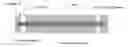
FIG. 1 is a cross sectional depiction of stacked semiconductor wafers with an adhesive disposed between the wafers showing the current state of the art.
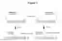
FIG. 2 is a cross sectional depiction of stacked semiconductor wafers with more than one adhesive disposed between the wafers showing the instant invention.
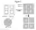
FIG. 3 depicts a topside view of a wafer with individual dies before and after dicing showing the use of two different adhesives.
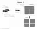
FIG. 4 is a depiction of wafer printing and coating, showing how deposition means work in the disposition of two different materials. The dicing lines and circuitry are not shown; the horizontal and vertical lines represent printed adhesive, encapsulant, or coating.
FIG. 5 shows the disposition of two different materials for wafer backside coatings.
FIG. 6 depicts the disposition of three different materials for through-vias in silicon dies.
FIG. 7 depicts selective applications for wire encapsulation .
FIG. 8 depicts the use of transparent material and high flow adhesive for image sensors and encapsulants.
FIG. 9 shows the use of the selective deposition method for fluxing agents and underfill encapsulants.
DETAILED DESCRIPTION OF THE INVENTION
In the fabrication of electronic devices, and in particular, in the fabrication of semiconductor wafers and dies, various types of adhesives, encapsulants, and coatings are used to impart functionality and to provide protection. These materials are applied by various means, in many instances by some form of printing, and in many cases, to the semiconductor wafer before it is singulated into individual dies.
The surfaces of the devices or semiconductors (also called “substrates” herein) are patterned with elements of circuitry. These circuitry elements and the surrounding areas form patterns and relate to specific functions in the operation of the semiconductor or device. In current practice, typically only one type of material is applied per layer (of adhesive, encapsulant, or coating) to impart functionality or protection.
In some situations, it would be preferable to be able to deposit more than one type of material per layer over the surface, thereby enhancing optimum performance over the totality of the surface, inasmuch as different areas of the surface are involved in different functions and have different performance requirements.
This is accomplished through the instant method of selectively printing, in which two or more printing heads, each containing a different material (such as, adhesive, coating, or encapsulant) used in the fabrication of the device or semiconductor to be printed, are used to deposit the material onto the surface of the device or semiconductor in a predetermined pattern consistent with the functionality of that part of the surface of the substrate. In one embodiment, the means of deposition is printing, and the printing means can be any that are effective for accomplishing the deposition of the particular material. Ink jet printing is one method that can be used to deposit material.
Applications in which the instant invention can be used are referenced in the Figures.
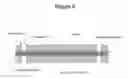
In the industry drive toward faster production, the stacking of semiconductor wafers for simultaneous dicing of all the wafers in the stack is becoming standard operation. An adhesive is used to hold the wafers aligned. If the adhesive is a low modulus adhesive, the centers of the dies diced from the wafer have lower stress and greater reliability; however, the edges of the dies relating to the dicing lines on the wafer suffer burring or chipping. If the adhesive is a high modulus, more brittle adhesive, the edges of the dies do not become burred or chipped; however, the center of the die is easily stressed and reliability decreases. This is shown in FIG. 1.
FIG. 2 depicts the solution to this problem and shows two stacked semiconductor wafers adhered together with a single layer of adhesive in which the adhesive along the dicing line is a high modulus adhesive, and the adhesive in the remaining area off the dicing line is a low modulus adhesive.
FIG. 3 is the topside view of the wafer showing bonding pads and dicing lines.
FIG. 4 is a depiction of how multiple sets of deposition means, in this figure two sets, each moving 90 degrees relative to the other, can be used to deposit different adhesives in one layer. Each deposition means will deposit one of the adhesives, encapsulants or coatings. The deposition means can be, for example, ink jet nozzles or blades.
The selective printing method may also be used to deposit any of the various protective materials used in the industry for wafer backside coatings. FIG. 5 is a depiction of the printing of a high modulus adhesive and a low modulus adhesive on the backside of a wafer, and the subsequent dicing of the wafer into individual dies.
Through-vias are pathways through a semiconductor die to accommodate the positioning of conductive leads from the bondpad on one surface of the die through to the surface of another die. In one embodiment in which dies are stacked, the via on one die leads from one surface to the other surface and to a conductive material on that other surface, and from there to another via in another die. This is shown in FIG. 6. The selective deposition method of this invention will permit the deposition of a high modulus adhesive along the dicing lines of the semi-conductor wafer from which the dies will be diced, the deposition of conductive material at the via openings for the dies, and the deposition of low modulus adhesive in the center of the die. These depositions typically will take place at the wafer level, with respect to patterns for singulating (dicing) the individual dies.
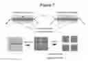
FIG. 7 is a depiction of mono-layer and multi-layer selective depositions for wire encapsulation. This type of selective deposition can be used in applications to protect wire bonding in die stacking arrangements. In die stacks, a high flow, high modulus adhesive can be applied to the wire bonding area, and a low flow, low modulus adhesive can be applied to the remainder of the semiconductor die for conventional bond line thickness and stress release.
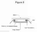
For image sensors, transparent filler materials are needed to protect and cover the image sensor and high flow adhesives are used to cover bonding wires. FIG. 8 is a depiction of an image sensor illustrating the placement of the transparent material and wire adhesive in one embodiment, which can be achieved by selective deposition in one layer.
Selective deposition can also be used for depositing fluxing agents and underfills for flip-chip devices. Fluxing agents can be deposited onto the solder ball pads on flip-chip devices, and underfill encapsulant can be deposited on the area surrounding the solder ball pads. This is shown in FIG. 9.
It is also possible to use selective deposition, particularly when jet printing is the means of deposition, to apply multiple layers of adhesive or coating in very thin thicknesses to accommodate tight tolerances.
Claims
1. A semiconductor substrate coated with a single layer of different materials selected from adhesives, coatings, and encapsulants.
2. The semiconductor substrate according to claim 1 in which the substrate comprises stacked semiconductor wafers with dicing lines, the wafers adhered together with a single layer of adhesive, in which the adhesive along the dicing lines is a high modulus adhesive, and the adhesive off the dicing lines is a low modulus adhesive.
3. The semiconductor substrate according to claim 1 in which the substrate comprises a semiconductor wafer with via openings and a die pattern formed with dicing lines, the semiconductor wafer coated with a high modulus adhesive along the dicing lines, a conductive material at the via openings, and a low modulus adhesive in the center of the die pattern formed by the dicing lines.
4. The semiconductor substrate according to claim 1 in which the substrate comprises a stack of semiconductor dies having wire bonds, in which a high flow, high modulus adhesive is applied to the wire bonds, and a low flow, low modulus adhesive is applied to the remainder of the semiconductor dies.
5. The semiconductor substrate according to claim 1 in which the substrate comprises an image sensor coated with a transparent filler material and wire bonds covered with a high flow adhesive.
6. The semiconductor substrate according to claim 1 in which the substrate comprises a flip-chip device containing solder ball pads in which a fluxing agent is coated onto the solder ball pads and an underfill encapsulant is coated on the area surrounding the solder ball pads.
Images & Drawings included:


Sources:
- United States Patent and Trademark Office - verify current appl. status at the USPTO↗
Recent applications in this class:
- » 20250167195 2025-05-22
REPAIR TECHNIQUES FOR MICRO-LED DEVICES AND ARRAYS - » 20250167194 2025-05-22
REPAIR TECHNIQUES FOR MICRO-LED DEVICES AND ARRAYS - » 20250158007 2025-05-15
METHOD OF MANUFACTURING A PACKAGE-ON-PACKAGE TYPE SEMICONDUCTOR PACKAGE - » 20250158006 2025-05-15
METHOD FOR MANUFACTURING SEMICONDUCTOR DEVICE WITH SUBSTRATE FOR ELECTRICAL CONNECTION - » 20250158005 2025-05-15
SEMICONDUCTOR DEVICE AND METHOD OF MANUFACTURE - » 20250140774 2025-05-01
BACK-TO-BACK SOLID STATE LIGHTING DEVICES AND ASSOCIATED METHODS - » 20250140773 2025-05-01
ELECTRONIC PACKAGE ASSEMBLY AND A METHOD FOR FORMING THE SAME - » 20250140772 2025-05-01
METHOD FOR BUILDING MODULES - » 20250112218 2025-04-03
SELECTIVE LAYER TRANSFER PROCESS IMPROVEMENTS - » 20250096220 2025-03-20
SEMICONDUCTOR PACKAGE STRUCTURE AND PACKAGING METHOD THEREOF