Semiconductor structure and fabrication method thereof
US20120280384A1
2012-11-08
13/167,086
2011-06-23
✅ Patent granted
US 8,866,293 B2
2014-10-21
-
-
Mark A Laurenzi
Edwards Wildman Palmer LLP | Peter F. Corless | Steven M. Jensen
2031-06-23
Abstract:
A fabrication method of a semiconductor structure includes providing a chip having at least an electrode pad, forming a titanium layer on the electrode pad, forming a dielectric layer on the chip and a portion of the titanium layer, forming a copper layer on the dielectric layer and the titanium layer, forming a conductive pillar on the copper layer corresponding in position to the titanium layer, and removing a portion of the copper layer that is not covered by the conductive pillar. When the portion of the copper layer is removed by etching, undercutting of the titanium layer is avoided since the titanium layer is covered by the dielectric layer, thereby providing an improved support for the conductive pillar to increase product reliability.
Inventors:
- Meng-Tsung Lee 15 🇹🇼 Taichung, Taiwan
- Yi-Hung Lin 12 🇹🇼 Taichung, Taiwan
- Sui-An Kao 4 🇹🇼 Taichung, Taiwan
- Yi-Hsin Chen 6 🇹🇼 Taichung, Taiwan
- Feng-Lung Chien 1 🇹🇼 Taiwan, Taiwan
Assignee:
- Siliconware Precision Industries Co., Ltd. 673 🇹🇼 Taichung, Taiwan
Applicant:
Interested in similar patents?
Get notified when new applications in this technology area are published.
Classification:
H01L2924/01074 » CPC further
Indexing scheme for arrangements or methods for connecting or disconnecting semiconductor or solid-state bodies as covered by; Chemical elements Tungsten [W]
H01L2224/03622 » CPC further
Indexing scheme for arrangements for connecting or disconnecting semiconductor or solid-state bodies and methods related thereto as covered by; Means for bonding being attached to, or being formed on, the surface to be connected, e.g. chip-to-package, die-attach, "first-level" interconnects; Manufacturing methods related thereto; Bonding areas; Manufacturing methods related thereto; Manufacturing methods by patterning a pre-deposited material using masks
H01L2224/03912 » CPC further
Indexing scheme for arrangements for connecting or disconnecting semiconductor or solid-state bodies and methods related thereto as covered by; Means for bonding being attached to, or being formed on, the surface to be connected, e.g. chip-to-package, die-attach, "first-level" interconnects; Manufacturing methods related thereto; Bonding areas; Manufacturing methods related thereto; Manufacturing methods; Methods of manufacturing bonding areas involving a specific sequence of method steps the bump being used as a mask for patterning the bonding area
H01L2224/116 » CPC further
Indexing scheme for arrangements for connecting or disconnecting semiconductor or solid-state bodies and methods related thereto as covered by; Means for bonding being attached to, or being formed on, the surface to be connected, e.g. chip-to-package, die-attach, "first-level" interconnects; Manufacturing methods related thereto; Bump connectors; Manufacturing methods related thereto; Manufacturing methods by patterning a pre-deposited material
H01L2924/01022 » CPC further
Indexing scheme for arrangements or methods for connecting or disconnecting semiconductor or solid-state bodies as covered by; Chemical elements Titanium [Ti]
H01L2924/0132 » CPC further
Indexing scheme for arrangements or methods for connecting or disconnecting semiconductor or solid-state bodies as covered by; Alloys Binary Alloys
H01L2924/014 » CPC further
Indexing scheme for arrangements or methods for connecting or disconnecting semiconductor or solid-state bodies as covered by; Alloys Solder alloys
H01L2224/0347 » CPC further
Indexing scheme for arrangements for connecting or disconnecting semiconductor or solid-state bodies and methods related thereto as covered by; Means for bonding being attached to, or being formed on, the surface to be connected, e.g. chip-to-package, die-attach, "first-level" interconnects; Manufacturing methods related thereto; Bonding areas; Manufacturing methods related thereto; Manufacturing methods using a lift-off mask
H01L24/13 » CPC further
Arrangements for connecting or disconnecting semiconductor or solid-state bodies; Methods or apparatus related thereto; Means for bonding being attached to, or being formed on, the surface to be connected, e.g. chip-to-package, die-attach, "first-level" interconnects; Manufacturing methods related thereto; Bump connectors ; Manufacturing methods related thereto; Structure, shape, material or disposition of the bump connectors prior to the connecting process of an individual bump connector
H01L2224/1161 » CPC further
Indexing scheme for arrangements for connecting or disconnecting semiconductor or solid-state bodies and methods related thereto as covered by; Means for bonding being attached to, or being formed on, the surface to be connected, e.g. chip-to-package, die-attach, "first-level" interconnects; Manufacturing methods related thereto; Bump connectors; Manufacturing methods related thereto; Manufacturing methods by patterning a pre-deposited material Physical or chemical etching
H01L2924/00014 » CPC further
Indexing scheme for arrangements or methods for connecting or disconnecting semiconductor or solid-state bodies as covered by; Technical content checked by a classifier the subject-matter covered by the group, the symbol of which is combined with the symbol of this group, being disclosed without further technical details
H01L21/283 IPC
Processes or apparatus adapted for the manufacture or treatment of semiconductor or solid state devices or of parts thereof; Manufacture or treatment of semiconductor devices or of parts thereof the devices having at least one potential-jump barrier or surface barrier, e.g. PN junction, depletion layer or carrier concentration layer the devices having semiconductor bodies comprising elements of Group IV of the Periodic System or AB compounds with or without impurities, e.g. doping materials; Manufacture of electrodes on semiconductor bodies using processes or apparatus not provided for in groups - Deposition of conductive or insulating materials for electrodes conducting electric current
H01L2924/01029 » CPC further
Indexing scheme for arrangements or methods for connecting or disconnecting semiconductor or solid-state bodies as covered by; Chemical elements Copper [Cu]
H01L2224/0556 » CPC further
Indexing scheme for arrangements for connecting or disconnecting semiconductor or solid-state bodies and methods related thereto as covered by; Means for bonding being attached to, or being formed on, the surface to be connected, e.g. chip-to-package, die-attach, "first-level" interconnects; Manufacturing methods related thereto; Bonding areas; Manufacturing methods related thereto; Structure, shape, material or disposition of the bonding areas prior to the connecting process of an individual bonding area; External layer Disposition
H01L2224/11849 » CPC further
Indexing scheme for arrangements for connecting or disconnecting semiconductor or solid-state bodies and methods related thereto as covered by; Means for bonding being attached to, or being formed on, the surface to be connected, e.g. chip-to-package, die-attach, "first-level" interconnects; Manufacturing methods related thereto; Bump connectors; Manufacturing methods related thereto; Manufacturing methods; Post-treatment of the bump connector; Thermal treatments, e.g. annealing, controlled cooling Reflowing
H01L2224/039 » CPC further
Indexing scheme for arrangements for connecting or disconnecting semiconductor or solid-state bodies and methods related thereto as covered by; Means for bonding being attached to, or being formed on, the surface to be connected, e.g. chip-to-package, die-attach, "first-level" interconnects; Manufacturing methods related thereto; Bonding areas; Manufacturing methods related thereto; Manufacturing methods Methods of manufacturing bonding areas involving a specific sequence of method steps
H01L2224/119 » CPC further
Indexing scheme for arrangements for connecting or disconnecting semiconductor or solid-state bodies and methods related thereto as covered by; Means for bonding being attached to, or being formed on, the surface to be connected, e.g. chip-to-package, die-attach, "first-level" interconnects; Manufacturing methods related thereto; Bump connectors; Manufacturing methods related thereto; Manufacturing methods Methods of manufacturing bump connectors involving a specific sequence of method steps
H01L24/03 » CPC main
Arrangements for connecting or disconnecting semiconductor or solid-state bodies; Methods or apparatus related thereto; Means for bonding being attached to, or being formed on, the surface to be connected, e.g. chip-to-package, die-attach, "first-level" interconnects; Manufacturing methods related thereto; Bonding areas ; Manufacturing methods related thereto Manufacturing methods
H01L2224/11462 » CPC further
Indexing scheme for arrangements for connecting or disconnecting semiconductor or solid-state bodies and methods related thereto as covered by; Means for bonding being attached to, or being formed on, the surface to be connected, e.g. chip-to-package, die-attach, "first-level" interconnects; Manufacturing methods related thereto; Bump connectors; Manufacturing methods related thereto; Manufacturing methods by blanket deposition of the material of the bump connector; Plating Electroplating
H01L2224/0361 » CPC further
Indexing scheme for arrangements for connecting or disconnecting semiconductor or solid-state bodies and methods related thereto as covered by; Means for bonding being attached to, or being formed on, the surface to be connected, e.g. chip-to-package, die-attach, "first-level" interconnects; Manufacturing methods related thereto; Bonding areas; Manufacturing methods related thereto; Manufacturing methods by patterning a pre-deposited material Physical or chemical etching
H01L23/00 IPC
Details of semiconductor or other solid state devices
H01L23/31 IPC
Details of semiconductor or other solid state devices; Encapsulations, e.g. encapsulating layers, coatings, e.g. for protection characterised by the arrangement or shape
H01L2224/0401 » CPC further
Indexing scheme for arrangements for connecting or disconnecting semiconductor or solid-state bodies and methods related thereto as covered by; Means for bonding being attached to, or being formed on, the surface to be connected, e.g. chip-to-package, die-attach, "first-level" interconnects; Manufacturing methods related thereto; Bonding areas; Manufacturing methods related thereto; Structure, shape, material or disposition of the bonding areas prior to the connecting process Bonding areas specifically adapted for bump connectors, e.g. under bump metallisation [UBM]
H01L23/3192 » CPC further
Details of semiconductor or other solid state devices; Encapsulations, e.g. encapsulating layers, coatings, e.g. for protection characterised by the arrangement or shape; Partial encapsulation or coating Multilayer coating
H01L2224/03901 » CPC further
Indexing scheme for arrangements for connecting or disconnecting semiconductor or solid-state bodies and methods related thereto as covered by; Means for bonding being attached to, or being formed on, the surface to be connected, e.g. chip-to-package, die-attach, "first-level" interconnects; Manufacturing methods related thereto; Bonding areas; Manufacturing methods related thereto; Manufacturing methods; Methods of manufacturing bonding areas involving a specific sequence of method steps with repetition of the same manufacturing step
H01L24/05 » CPC further
Arrangements for connecting or disconnecting semiconductor or solid-state bodies; Methods or apparatus related thereto; Means for bonding being attached to, or being formed on, the surface to be connected, e.g. chip-to-package, die-attach, "first-level" interconnects; Manufacturing methods related thereto; Bonding areas ; Manufacturing methods related thereto; Structure, shape, material or disposition of the bonding areas prior to the connecting process of an individual bonding area
H01L2224/0345 » CPC further
Indexing scheme for arrangements for connecting or disconnecting semiconductor or solid-state bodies and methods related thereto as covered by; Means for bonding being attached to, or being formed on, the surface to be connected, e.g. chip-to-package, die-attach, "first-level" interconnects; Manufacturing methods related thereto; Bonding areas; Manufacturing methods related thereto; Manufacturing methods by blanket deposition of the material of the bonding area in gaseous form Physical vapour deposition [PVD], e.g. evaporation, or sputtering
H01L24/11 » CPC main
Arrangements for connecting or disconnecting semiconductor or solid-state bodies; Methods or apparatus related thereto; Means for bonding being attached to, or being formed on, the surface to be connected, e.g. chip-to-package, die-attach, "first-level" interconnects; Manufacturing methods related thereto; Bump connectors ; Manufacturing methods related thereto Manufacturing methods
H01L23/48 IPC
Details of semiconductor or other solid state devices Arrangements for conducting electric current to or from the solid state body in operation, e.g. leads, terminal arrangements ; Selection of materials therefor
Description
BACKGROUND OF THE INVENTION
1. Field of the Invention
The present invention relates to semiconductor structures and fabrication methods thereof, and, more particularly, to a semiconductor structure having conductive pillars and a fabrication method thereof.
2. Description of Related Art
Electronic products are becoming lighter, thinner and smaller, as well as developed for high performance and multi-functionality. There are various types of semiconductor chip packages, such as wire bonding type packages, flip-chip type packages and so on. Compared with wire bonding type packages, flip-chip type packages are advantageous in reducing the overall volume of semiconductor devices.
A fabrication method of a flip-chip type package generally involves electrically connecting an active surface of a chip to conductive pads of a packaging substrate through a plurality of conductive bumps, and filling an underfill between the active surface of the semiconductor chip and the substrate for encapsulating the conductive bumps. Therein, the material of the conductive bumps greatly affects the flip-chip alignment accuracy.
U.S. Pat. Nos. 7,863,740 and 7,804,173 disclose methods for electrically connecting a semiconductor chip with a packaging substrate through copper pillars.
Referring to FIG. 1A, a semiconductor chip 10 having at least an electrode pad 100 is provided. The outer surface of the semiconductor chip 10 is made of a silicon nitride layer, which has an opening for exposing the electrode pad 100, respectively.
Then, a dielectric layer 12 is formed on the silicon nitride layer 101 and around the wall of the opening of the silicon nitride layer 101. Subsequently, a titanium layer 11 is formed to cover the entire surface of the dielectric layer 12 and the electrode pad 100. Further, a copper layer 13 is formed to cover the entire surface of the titanium layer 11.
Referring to FIG. 1B, a resist layer 14 is formed on the copper layer 13 and an open area 140 is formed in the resist layer 14 for exposing a portion of the copper layer 13. Then, a copper pillar 15 is formed on the exposed portion of the copper layer 13 and a solder material 16 is formed on a top surface of the copper pillar 15.
Referring to FIG. 1C, the resist layer 14 is removed to expose a portion of the copper layer 13.
Referring to FIG. 1D, using the copper pillar 15 as an etch stop layer, an etching process is performed to remove the exposed portion of the copper layer 13 and the titanium layer 11 under the exposed portion of the copper layer 13. Thereafter, a solder bump can be formed on the copper pillar 15 and the solder material 16, and then a reflow process can be performed so as to form a conductive bump electrically connecting the chip 10 and a packaging substrate (not shown).
Since the copper pillar 15 does not deform during the reflow process, melting and collapsing of the copper pillar 15 can be prevented, thereby avoiding position deviation of the chip 10 and increasing position alignment accuracy of the chip 10.
However, since the etching process using an etching solution is isotropic, when the copper layer 13 and the titanium layer 11 under the copper layer 13 are partially removed by etching, an undercut of the titanium layer 11 can occur, as shown at position K of FIG. 1D, thus resulting in an insufficient support for the copper pillar 15 and reducing the reliability of the conductive bump.
Therefore, there is a need to provide a semiconductor structure and a fabrication method thereof so as to overcome the above-described drawback.
SUMMARY OF THE INVENTION
Accordingly, the present invention provides a fabrication method of a semiconductor structure, which comprises the steps of: providing a chip having at least an electrode pad; forming a first metal layer on the electrode pad; forming a dielectric layer on the chip and the first metal layer, the dielectric layer having an opening for exposing a portion of the first metal layer; forming a second metal layer on the dielectric layer and the exposed portion of the first metal layer, the material of the first metal layer being different from that of the second metal layer; forming a conductive pillar on the second metal layer corresponding in position to the first metal layer; and removing a portion of the second metal layer that is not covered by the conductive pillar and preserving the remaining portion of the second metal layer covered by the conductive pillar.
The above-described method forms the first metal layer first and then forms the dielectric layer so as to define the size of the first metal layer before forming the second metal layer. Therefore, when the second metal layer is partially removed by etching, undercutting of the first metal layer can be avoided since the first metal layer is covered by the dielectric layer.
According to the above-described method, the present invention further provides a semiconductor structure, which comprises: a chip having at least an electrode pad; a first metal layer formed on the electrode pad; a dielectric layer formed on the chip and the first metal layer and having an opening for exposing a portion of the first metal layer; a second metal layer formed on the exposed portion of the first metal layer and the dielectric layer therearound, the material of the first metal layer being different from that of the second metal layer; and a conductive pillar disposed on the second metal layer.
In another aspect, the present invention provides a fabrication method of a semiconductor structure, which comprises: providing a chip having at least an electrode pad; forming a first metal layer on the electrode pad; forming a second metal layer on the first metal layer, the material of the first metal layer being different from that of the second metal layer; forming a conductive pillar on the second metal layer corresponding in position to the first metal layer, the first metal layer having an area larger than the sectional area of the conductive pillar; and removing a portion of the second metal layer that is not covered by the conductive pillar and preserving the remaining portion of the second metal layer covered by the conductive pillar.
When the second metal layer is partially removed by etching, since the area of the first metal layer is larger than the sectional area of the conductive pillar, undercutting of the first metal layer can be avoided. That is, instead of completely positioning the titanium layer under a copper pillar as in the prior art, a portion of the first metal layer is exposed from the conductive pillar even if the first metal layer experiences an isotropic etching process.
According to the above-described method, the present invention provides another semiconductor structure, which comprises: a chip having at least an electrode pad; a first metal layer formed on the electrode pad; a second metal layer formed on the first metal layer, the material of the first metal layer being different from that of the second metal layer; and a conductive pillar disposed on the second metal layer, the first metal layer having an area larger than the sectional area of the conductive pillar.
BRIEF DESCRIPTION OF DRAWINGS
FIGS. 1A to 1D are cross-sectional views showing a fabrication method of a semiconductor structure in the prior art;
FIGS. 2A to 2G are cross-sectional views showing a fabrication method of a semiconductor structure according to a first embodiment of the present invention; and
FIGS. 3A to 3D are cross-sectional views showing a fabrication method of a semiconductor structure according to a second embodiment of the present invention.
DETAILED DESCRIPTION OF PREFERRED EMBODIMENTS
The following illustrative embodiments are provided to illustrate the disclosure of the present invention and its advantages, these and other advantages and effects will be apparent to those in the art after reading this specification.
It should be noted that the drawings are not intended to limit the present invention. Various modification and variations can be made without departing from the spirit of the present invention. Further, terms such as “one”, “above” and so on are merely for illustrative purpose and should not be construed to limit the scope of the present invention.
First Embodiment
FIGS. 2A to 2G are cross-sectional views showing a fabrication method of a semiconductor structure according to a first embodiment of the present invention.
Referring to FIG. 2A, a semiconductor chip 20 having at least an electrode pad 200 made of, for example, aluminum is provided. The outer surface of the semiconductor chip 20 is made of, for example, a silicon nitride layer 201 and has an opening for exposing the electrode pad 200. There are various pertinent chip structures in the art and detailed description thereof is omitted herein for brevity.
Referring to FIG. 2B(b), a first metal layer 21a, such as a titanium layer or a titanium tungsten layer, is formed on the electrode pad 200 and the silicon nitride layer 201 therearound.
In the present embodiment, the first metal layer is formed through a patterning process. First, as shown in FIG. 2B(a), a first metal material 21 is formed on the electrode pad 200 and the entire surface of the silicon nitride layer 201 by sputtering. Then, a resist layer 210 is formed to cover a portion of the first metal material 21 located on the electrode pad 200 and the silicon nitride layer 201 around the electrode pad 200. Referring to FIG. 2B(b), the remaining portion of the first metal material 21 that is not covered by the resist layer 210 is removed by etching and then the resist layer 210 is removed to obtain a first metal layer 21a. The resist layer 210 can be made of photoresist, and open areas of the resist layer 210 for partially exposing the first metal material 21 can be formed by exposure and development. It should be noted that various patterning processes in the art can be applied in the present invention and detailed description thereof is omitted herein.
Referring to FIG. 2C, a dielectric layer 22 is formed on the silicon nitride layer 201 and the first metal layer 21a and an opening 220 is formed in the dielectric layer 22 for exposing a portion of the first metal layer 21a.
In the present embodiment, the dielectric layer 22 is a polyimide layer, but is not limited thereto.
Referring to FIG. 2D, a second metal layer 23, such as a copper layer, is formed on the dielectric layer 22 and the exposed portion of the first metal layer 21a by sputtering.
Then, a resist layer 24 made of photoresist is formed on the second metal layer 23, and an open area 240 is formed in the resist layer 24 by exposure and development for exposing a portion of the second metal layer 23 corresponding in position to the first metal layer 21a. In the present embodiment, the open area 240 is larger than the area of the first metal layer 21a.
Referring to FIG. 2E, a conductive pillar 25 is formed on the second metal layer 23 in the open area 240 by electroplating. In the present embodiment, the conductive pillar 25 is a copper pillar.
Further, a conductive material 26 can be formed on a top surface of the conductive pillar 25. In the present embodiment, the conductive material 26 consists of a nickel material 260 and a solder material 261. In other embodiments, the conductive material 26 can be a solder material.
Referring to FIG. 2F, the resist layer 24 is removed to expose a portion of the second metal layer 23 that is not covered by the conductive pillar 25.
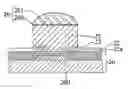
Referring to FIG. 2G, the exposed portion of the second metal layer 23 is removed by etching to expose the dielectric layer 22 around the conductive pillar 25. Meanwhile, the remaining portion of the second metal layer 23 that is covered by the conductive pillar 25 is preserved. Thus, a semiconductor structure is obtained. In subsequent processes, a solder bump can be formed on the conductive pillar 25 and the solder material 26 and then reflowed so as to form a conductive bump electrically connecting the semiconductor structure and a packaging substrate (not shown).
The semiconductor structure has a semiconductor chip 20 having at least an electrode pad 200, a first metal layer 21a formed on the electrode pad 200 and a surface of the chip 20 around the electrode pad 200, a first dielectric layer 22 formed on the chip 20 and the first metal layer 21 a and having an opening 220 for exposing a portion of the first metal layer 21a, a second metal layer 23 formed on the exposed portion of the first metal layer 21a and the dielectric layer 22 therearound, and a conductive pillar 25 disposed on the second metal layer 23. Therein, the material of the first metal layer 21a (for example, titanium) is different from the material of the second metal layer 23 (for example, copper). The semiconductor structure further has a conductive material 26 disposed on a top surface of the conductive pillar 25.
The present invention defines the size of the first metal layer 21a before forming the dielectric layer 22 and the second metal layer 23. When the exposed portion of the second metal layer 23 is removed by etching, undercutting of the first metal layer 21a can be avoided since the first metal layer 21a is covered by the dielectric layer 22, thereby providing sufficient support to the conductive pillar 25 and accordingly increasing the reliability of the subsequently formed conductive bump.
Second Embodiment
FIGS. 3A to 3D are cross-sectional views showing a fabrication method of a semiconductor structure according to a second embodiment of the present invention. Compared with the first embodiment, the dielectric layer and the first metal layer of the present embodiment are fabricated in a different sequence. Related processes are described as follows.
Referring to FIG. 3A, continuing from FIG. 2A, a dielectric layer 22′ is formed on the silicon nitride layer 201 and the electrode pad 200 of the chip 20 and has an opening 220′ for exposing the electrode pad 200.
Referring to FIG. 3B, a first metal layer 21a′ is formed on the electrode pad 200 and the dielectric layer 22′ around the electrode pad 200 by patterning.
Referring to FIG. 3C, a second metal layer 23 is formed on the dielectric layer 22′ and the first metal layer 21a.
Then, a conductive pillar 25 is formed on the second metal layer 23 corresponding in position to the first metal layer 21a′ by patterning. The first metal layer 21a′ has an area A larger than the sectional area S of the conductive pillar 25.
Referring to FIG. 3D, a portion of the second metal layer 23 that is not covered by the conductive pillar 25 is removed and the remaining portion of the second metal layer 23 covered by the conductive pillar 25 is preserved, thus obtaining a semiconductor structure. Subsequently, a conductive bump can be formed through a reflow process for electrically connecting the semiconductor structure and a packaging substrate.
The semiconductor structure has a semiconductor chip 20 having at least an electrode pad 200, a dielectric layer 22 formed on the chip 20 and the electrode pad 200 and having an opening 220′ for exposing the electrode pad 200, a first metal layer 21a′ formed on the electrode pad 200 and the dielectric layer 22′ around the electrode pad 200, a second metal layer 23 formed on the first metal layer 21a′, and a conductive pillar 25 disposed on the second metal layer 23. Therein, the first metal layer 21a′ has an area A larger than the sectional area S of the conductive pillar 25. The material of the first metal layer 21a′ (for example, titanium) is different from the material of the second metal layer 23 (for example, copper). The semiconductor structure further has a conductive material 26 disposed on a top surface of the conductive pillar 25.
In the present embodiment, during etching of the second metal layer 23, since the first metal layer 21a′ has an area A larger than the sectional area S of the conductive pillar 25, even if the first metal layer 21a′ experiences isotropic etching, the first metal layer 21a′ is still exposed on the dielectric layer 22′, thereby avoiding an undercut as in the prior art so as to provide sufficient support for the conductive pillar 25 and increase the reliability of the conductive bump.
The above-described descriptions of the detailed embodiments are provided to illustrate the preferred implementation according to the present invention, not to limit the scope of the present invention. Accordingly, numerous modifications and variations completed by those with ordinary skill in the art will fall within the scope of present invention as defined by the appended claims.
Claims
What is claimed is:1. A semiconductor structure, comprising:
a chip having at least an electrode pad;
a first metal layer formed on the at least an electrode pad;
a dielectric layer formed on the chip and the first metal layer and having an opening for exposing a portion of the first metal layer;
a second metal layer formed on the exposed portion of the first metal layer and the dielectric layer therearound, the first metal layer being different in material from the second metal layer; and
a conductive pillar disposed on the second metal layer.
2. The structure of claim 1, wherein the first metal layer is a titanium layer or a titanium tungsten layer.
3. The structure of claim 1, wherein the first metal layer extends to a surface of the chip around the at least an electrode pad.
4. The structure of claim 1, wherein the second metal layer is a copper layer.
5. The structure of claim 1, wherein the conductive pillar is a copper pillar.
6. The structure of claim 1, further comprising a conductive material formed on a top surface of the conductive pillar.
7. A semiconductor structure, comprising:
a chip having at least an electrode pad;
a first metal layer formed on the at least an electrode pad;
a second metal layer formed on the first metal layer, the first metal layer being different in material from the second metal layer; and
a conductive pillar disposed on the second metal layer, the first metal layer having an area larger than a sectional area of the conductive pillar.
8. The structure of claim 7, wherein the first metal layer is a titanium layer or a titanium tungsten layer.
9. The structure of claim 7, further comprising a dielectric layer formed on the chip and the electrode pad and having an opening for exposing the electrode pad so as to allow the first metal layer to be formed thereon.
10. The structure of claim 9, wherein the first metal layer extends to a surface of the dielectric layer around the electrode pad.
11. The structure of claim 7, wherein the second metal layer is a copper layer.
12. The structure of claim 7, wherein the conductive pillar is a copper pillar.
13. The structure of claim 7, further comprising a conductive material formed on a top surface of the conductive pillar.
14. A fabrication method of a semiconductor structure, comprising the steps of:
providing a chip having at least an electrode pad;
forming a first metal layer on the electrode pad;
forming a dielectric layer on the chip and the first metal layer, the dielectric layer having an opening for exposing a portion of the first metal layer;
forming a second metal layer on the dielectric layer and the exposed portion of the first metal layer, the first metal layer being different in material from the second metal layer;
forming a conductive pillar on the second metal layer corresponding in position to the first metal layer; and
removing a portion of the second metal layer that is not covered by the conductive pillar and preserving the remaining portion of the second metal layer covered by the conductive pillar.
15. The method of claim 14, wherein the first metal layer is a titanium layer or a titanium tungsten layer.
16. The method of claim 14, wherein forming the first metal layer comprises:
forming a first metal material on the electrode pad and a surface of the chip;
forming a resist layer to cover a portion of the first metal material located on the electrode pad and the surface of the chip around the electrode pad;
removing the remaining portion of the first metal material that is not covered by the resist layer; and
removing the resist layer.
17. The method of claim 14, wherein the second metal layer is a copper layer.
18. The method of claim 14, wherein the conductive pillar is a copper pillar.
19. The method of claim 14, further comprising, before removing the portion of the second metal layer that is not covered by the conductive pillar, forming a conductive material on a top surface of the conductive pillar.
20. A fabrication method of a semiconductor structure, comprising:
providing a chip having at least an electrode pad;
forming a first metal layer on the electrode pad;
forming a second metal layer on the first metal layer, the first metal layer being different in material from the second metal layer;
forming a conductive pillar on the second metal layer corresponding in position to the first metal layer, the first metal layer having an area larger than a sectional area of the conductive pillar; and
removing a portion of the second metal layer that is not covered by the conductive pillar and preserving the remaining portion of the second metal layer covered by the conductive pillar.
21. The method of claim 20, wherein the first metal layer is a titanium layer or a titanium tungsten layer.
22. The method of claim 20, further comprising, before forming the first metal layer on the electrode pad, forming a dielectric layer on the chip and the electrode pad, the dielectric layer having an opening for exposing the electrode pad.
23. The method of claim 22, wherein the first metal layer is further formed on a surface of the dielectric layer around the electrode pad.
24. The method of claim 22, wherein forming the first metal layer comprises:
forming a first metal material on the electrode pad and the dielectric layer;
forming a resist layer to cover a portion of the first metal material located on the electrode pad and a surface of the chip around the electrode pad;
removing the remaining portion of the first metal material that is not covered by the resist layer; and
removing the resist layer.
25. The method of claim 22, wherein the second metal layer is further formed on the dielectric layer.
26. The method of claim 20, wherein the second metal layer is a copper layer.
27. The method of claim 20, wherein the conductive pillar is a copper pillar.
28. The method of claim 20, further comprising, before removing the portion of the second metal layer that is not covered by the conductive pillar, forming a conductive material on a top surface of the conductive pillar.
Images & Drawings included:


Sources:
- United States Patent and Trademark Office - verify current appl. status at the USPTO↗
Similar patent applications:
- » 20240389296
SEMICONDUCTOR STRUCTURE, FABRICATION METHOD THEREOF, MEMORY AND MEMORY SYSTEM - » 20240389301
SEMICONDUCTOR STRUCTURE, FABRICATION METHOD THEREOF, AND MEMORY SYSTEM - » 20240389324
SEMICONDUCTOR STRUCTURE, FABRICATION METHOD THEREOF, AND MEMORY SYSTEM - » 20240222124
SEMICONDUCTOR STRUCTURE, METHOD FOR FABRICATING THEREOF, AND METHOD FOR FABRICATING SEMICONDUCTOR LAYOUT - » 20230049202
Semiconductor structure, method for fabricating thereof, and method for fabricating semiconductor layout - » 20240274531
SEMICONDUCTOR STRUCTURE, METHOD FOR FABRICATING THEREOF, AND METHOD FOR FABRICATING SEMICONDUCTOR LAYOUT - » 20070181990
Stacked semiconductor structure and fabrication method thereof - » 20070069337
Semiconductor structure and fabricating method thereof - » 20090128993
MULTI-TIER CAPACITOR STRUCTURE, FABRICATION METHOD THEREOF AND SEMICONDUCTOR SUBSTRATE EMPLOYING THE SAME - » 15236533
Semiconductor structure and fabricating method thereof
Recent applications in this class:
- » 20250286005 2025-09-11
SEMICONDUCTOR DEVICE, AND MANUFACTURING METHOD FOR SAME - » 20250218991 2025-07-03
FLIP CHIP PACKAGE ASSEMBLY HAVING POST CONNECTS WITH SOLDER-BASED JOINTS - » 20250149485 2025-05-08
METAL BUMPS AND METHOD FORMING SAME - » 20250149484 2025-05-08
SEMICONDUCTOR DEVICE INCLUDING BUMPS AND METHOD OF MANUFACTURING THE SAME - » 20250140724 2025-05-01
Multiple Polymer Layers as the Encapsulant of Conductive Vias - » 20250125294 2025-04-17
SEMICONDUCTOR DEVICE ASSEMBLY WITH SACRIFICIAL PILLARS AND METHODS OF MANUFACTURING SACRIFICIAL PILLARS - » 20250096173 2025-03-20
SHEET FOR FORMING FIRST PROTECTIVE MEMBRANE, METHOD FOR MANUFACTURING SEMICONDUCTOR DEVICE, AND USE OF SHEET - » 20250087610 2025-03-13
ELECTRONIC CHIP WITH CONNECTING PILLARS FOR SINTERING ASSEMBLY - » 20250079367 2025-03-06
METHOD FOR PRODUCING A SUBSTRATE HAVING A NANOPOROUS BUMP AND CORRESPONDING COMPONENT HAVING A SUBSTRATE WITH NANOPOROUS BUMP - » 20250070067 2025-02-27
ENABLING MICRO-BUMP ARCHITECTURES WITHOUT THE USE OF SACRIFICIAL PADS FOR PROBING A WAFER
Recent applications for this Assignee:
- » 20250046771 2025-02-06
METHOD FOR FABRICATING ELECTRONIC PACKAGE - » 20250015054 2025-01-09
CARRYING SUBSTRATE, ELECTRONIC PACKAGE HAVING THE CARRYING SUBSTRATE, AND METHODS FOR MANUFACTURING THE SAME - » 20240379534 2024-11-14
ELECTRONIC PACKAGE, MANUFACTURING METHOD FOR THE SAME, AND ELECTRONIC STRUCTURE - » 20240321798 2024-09-26
Electronic package and carrier thereof and method for manufacturing the same - » 20240321784 2024-09-26
Electronic package including lead frame having multiple conductive posts - » 20240321591 2024-09-26
METHOD FOR FABRICATING ELECTRONIC PACKAGE - » 20240290701 2024-08-29
ELECTRONIC PACKAGE AND MANUFACTURING METHOD THEREOF - » 20240290675 2024-08-29
Electronic package and manufacturing method thereof - » 20240290674 2024-08-29
ELECTRONIC PACKAGE AND MANUFACTURING METHOD THEREOF - » 20240282674 2024-08-22
ELECTRONIC PACKAGE AND METHOD OF FABRICATING THE SAME