Group III nitride wafer and its production method
US20140065796A1
2014-03-06
13/835,636
2013-03-15
✅ Patent granted
US 8,921,231 B2
2014-12-30
-
-
Bradley K Smith
K&L Gates LLP
2033-03-15
Abstract:
The present invention discloses a group III nitride wafer such as GaN, AlN, InN and their alloys having one surface visually distinguishable from the other surface. After slicing of the wafer from a bulk crystal of group III nitride with a mechanical method such as multiple wire saw, the wafer is chemically etched so that one surface of the wafer is visually distinguishable from the other surface. The present invention also discloses a method of producing such wafers.
Inventors:
- Tadao Hashimoto 76 🇺🇸 Santa Barbara, CA, United States
- Edward Letts 36 🇺🇸 Buellton, CA, United States
- Sierra HOFF 6 🇺🇸 Solvang, CA, United States
Assignee:
- Seoul Semiconductor Co., Ltd. 197 🇰🇷 Seoul, South Korea
- SixPoint Materials, Inc. 53 🇺🇸 Buellton, CA, United States
Applicant:
Interested in similar patents?
Get notified when new applications in this technology area are published.
Classification:
H01L29/2003 » CPC main
Semiconductor devices adapted for rectifying, amplifying, oscillating or switching, or capacitors or resistors with at least one potential-jump barrier or surface barrier, e.g. PN junction depletion layer or carrier concentration layer; Details of semiconductor bodies or of electrodes thereof; Multistep manufacturing processes therefor; Semiconductor bodies ; Multistep manufacturing processes therefor characterised by the materials of which they are formed including, apart from doping materials or other impurities, only AB compounds Nitride compounds
H01L29/20 IPC
Semiconductor devices adapted for rectifying, amplifying, oscillating or switching, or capacitors or resistors with at least one potential-jump barrier or surface barrier, e.g. PN junction depletion layer or carrier concentration layer; Details of semiconductor bodies or of electrodes thereof; Multistep manufacturing processes therefor; Semiconductor bodies ; Multistep manufacturing processes therefor characterised by the materials of which they are formed including, apart from doping materials or other impurities, only AB compounds
C30B7/105 » CPC further
Single-crystal growth from solutions using solvents which are liquid at normal temperature, e.g. aqueous solutions by application of pressure, e.g. hydrothermal processes using ammonia as solvent, i.e. ammonothermal processes
H01L21/02013 » CPC further
Processes or apparatus adapted for the manufacture or treatment of semiconductor or solid state devices or of parts thereof; Manufacture or treatment of semiconductor devices or of parts thereof; Preparing wafers; Preparing bulk and homogeneous wafers; Multistep processes; Specific process step Grinding, lapping
H01L21/461 IPC
Processes or apparatus adapted for the manufacture or treatment of semiconductor or solid state devices or of parts thereof; Manufacture or treatment of semiconductor devices or of parts thereof the devices having at least one potential-jump barrier or surface barrier, e.g. PN junction, depletion layer or carrier concentration layer the devices having semiconductor bodies not provided for in groups, , , and with or without impurities, e.g. doping materials; Treatment of semiconductor bodies using processes or apparatus not provided for in groups to change their surface-physical characteristics or shape, e.g. etching, polishing, cutting
C30B29/403 » CPC further
Single crystals or homogeneous polycrystalline material with defined structure characterised by the material or by their shape; Inorganic compounds or compositions; AB compounds wherein A is B, Al, Ga, In or Tl and B is N, P, As, Sb or Bi A-nitrides
H01L21/02019 » CPC further
Processes or apparatus adapted for the manufacture or treatment of semiconductor or solid state devices or of parts thereof; Manufacture or treatment of semiconductor devices or of parts thereof; Preparing wafers; Preparing bulk and homogeneous wafers; Multistep processes; Specific process step Chemical etching
C30B29/406 » CPC further
Single crystals or homogeneous polycrystalline material with defined structure characterised by the material or by their shape; Inorganic compounds or compositions; AB compounds wherein A is B, Al, Ga, In or Tl and B is N, P, As, Sb or Bi; A-nitrides Gallium nitride
H01L29/201 » CPC main
Semiconductor devices adapted for rectifying, amplifying, oscillating or switching, or capacitors or resistors with at least one potential-jump barrier or surface barrier, e.g. PN junction depletion layer or carrier concentration layer; Details of semiconductor bodies or of electrodes thereof; Multistep manufacturing processes therefor; Semiconductor bodies ; Multistep manufacturing processes therefor characterised by the materials of which they are formed including, apart from doping materials or other impurities, only AB compounds including two or more compounds, e.g. alloys
C30B7/10 IPC
Single-crystal growth from solutions using solvents which are liquid at normal temperature, e.g. aqueous solutions by application of pressure, e.g. hydrothermal processes
C30B29/40 IPC
Single crystals or homogeneous polycrystalline material with defined structure characterised by the material or by their shape; Inorganic compounds or compositions AB compounds wherein A is B, Al, Ga, In or Tl and B is N, P, As, Sb or Bi
C30B33/10 » CPC further
After-treatment of single crystals or homogeneous polycrystalline material with defined structure; Etching in solutions or melts
H01L21/02 IPC
Processes or apparatus adapted for the manufacture or treatment of semiconductor or solid state devices or of parts thereof Manufacture or treatment of semiconductor devices or of parts thereof
C30B33/00 » CPC further
After-treatment of single crystals or homogeneous polycrystalline material with defined structure
Description
CROSS REFERENCE TO RELATED APPLICATIONS
This application claims priority to U.S. App. No. 61/694,119 filed Aug. 28, 2012, by inventors Tadao Hashimoto, Edward Letts, and Sierra Hoff, entitled “GROUP III NITRIDE WAFER AND ITS PRODUCTION METHOD”, which is incorporated by reference in its entirety as if put forth in full below.
This application is related to the following U.S. patent applications:
PCT Utility Patent Application Serial No. US2005/024239, filed on Jul. 8, 2005, by Kenji Fujito, Tadao Hashimoto and Shuji Nakamura, entitled “METHOD FOR GROWING GROUP III-NITRIDE CRYSTALS IN SUPERCRITICAL AMMONIA USING AN AUTOCLAVE,” attorneys' docket number 30794.0129-WO-01 (2005-339-1);
U.S. Utility patent application Ser. No. 11/784,339, filed on Apr. 6, 2007, by Tadao Hashimoto, Makoto Saito, and Shuji Nakamura, entitled “METHOD FOR GROWING LARGE SURFACE AREA GALLIUM NITRIDE CRYSTALS IN SUPERCRITICAL AMMONIA AND LARGE SURFACE AREA GALLIUM NITRIDE CRYSTALS,” attorneys docket number 30794.179-US-U1 (2006-204), which application claims the benefit under 35 U.S.C. Section 119(e) of U.S. Provisional Patent Application Ser. No. 60/790,310, filed on Apr. 7, 2006, by Tadao Hashimoto, Makoto Saito, and Shuji Nakamura, entitled “METHOD FOR GROWING LARGE SURFACE AREA GALLIUM NITRIDE CRYSTALS IN SUPERCRITICAL AMMONIA AND LARGE SURFACE AREA GALLIUM NITRIDE CRYSTALS,” attorneys docket number 30794.179-US-P1 (2006-204);
U.S. Utility Patent Application Ser. No. 60/973,662, filed on Sep. 19, 2007, by Tadao Hashimoto and Shuji Nakamura, entitled “GALLIUM NITRIDE BULK CRYSTALS AND THEIR GROWTH METHOD,” attorneys docket number 30794.244-US-P1 (2007-809-1);
U.S. Utility patent application Ser. No. 11/977,661, filed on Oct. 25, 2007, by Tadao Hashimoto, entitled “METHOD FOR GROWING GROUP III-NITRIDE CRYSTALS IN A MIXTURE OF SUPERCRITICAL AMMONIA AND NITROGEN, AND GROUP III-NITRIDE CRYSTALS GROWN THEREBY,” attorneys docket number 30794.253-US-U1 (2007-774-2);
U.S. Utility Patent Application Ser. No. 61/067,117, filed on Feb. 25, 2008, by Tadao Hashimoto, Edward Letts, Masanori Ikari, entitled “METHOD FOR PRODUCING GROUP III-NITRIDE WAFERS AND GROUP III-NITRIDE WAFERS,” attorneys docket number 62158-30002.00;
U.S. Utility Patent Application Ser. No. 61/058,900, filed on Jun. 4, 2008, by Edward Letts, Tadao Hashimoto, Masanori Ikari, entitled “METHODS FOR PRODUCING IMPROVED CRYSTALLINITY GROUP III-NITRIDE CRYSTALS FROM INITIAL GROUP III-NITRIDE SEED BY AMMONOTHERMAL GROWTH,” attorneys docket number 62158-30004.00;
U.S. Utility Patent Application Ser. No. 61/058,910, filed on Jun. 4, 2008, by Tadao Hashimoto, Edward Letts, Masanori Ikari, entitled “HIGH-PRESSURE VESSEL FOR GROWING GROUP III NITRIDE CRYSTALS AND METHOD OF GROWING GROUP III NITRIDE CRYSTALS USING HIGH-PRESSURE VESSEL AND GROUP III NITRIDE CRYSTAL,” attorneys docket number 62158-30005.00;
U.S. Utility Patent Application Ser. No. 61/131,917, filed on Jun. 12, 2008, by Tadao Hashimoto, Masanori Ikari, Edward Letts, entitled “METHOD FOR TESTING III-NITRIDE WAFERS AND III-NITRIDE WAFERS WITH TEST DATA,” attorneys docket number 62158-30006.00;
which applications are incorporated by reference herein in their entirety as if put forth in full below.
BACKGROUND
1. Field of the Invention
The invention is related to a semiconductor wafer used for various device fabrication including optoelectronic and electronic devices such as light emitting diodes, (LEDs), laser diodes (LDs), photo detectors, and transistors. More specifically, the invention is on a compound semiconductor wafer composed of group III nitride.
2. Description of the Existing Technology
(Note: This patent application refers several publications and patents as indicated with numbers within brackets, e.g., [x]. A list of these publications and patents can be found in the section entitled “References.”)
Gallium nitride (GaN) and its related group III nitride alloys are the key material for various optoelectronic and electronic devices such as LEDs, LDs, microwave power transistors and solar-blind photo detectors. However, the majority of these devices are grown epitaxially on heterogeneous substrates (or wafers), such as sapphire and silicon carbide since GaN wafers are extremely expensive compared to these heteroepitaxial substrates. The heteroepitaxial growth of group III nitride causes highly defected or even cracked films, which hinder the realization of high-end electronic devices, such high-power microwave transistors.
To solve all fundamental problems caused by heteroepitaxy, it is indispensable to utilize group III nitride wafers sliced from group III nitride bulk crystals. For the majority of devices, GaN wafers are favorable because it is relatively easy to control the conductivity of the wafer and GaN wafer will provide the smallest lattice/thermal mismatch with most of device layers. However, due to the high melting point and high nitrogen vapor pressure at elevated temperature, it has been difficult to grow bulk GaN crystals. Currently, majority of commercially available GaN wafers are produced by a method called hydride vapor phase epitaxy (HVPE). HVPE is a vapor phase epitaxial film growth, thus difficult to produce bulk-shaped group III nitride crystals. Due to limitation of the crystal thickness, the typical density of line defects (e.g. dislocations) and grain boundaries is at the order of high 105 to low −106 cm−2.
To obtain high-quality GaN wafers of which density of dislocations and/or grain boundaries is less than 106 cm−2, a new method called ammonothermal growth has been developed [1-6]. Also, there are other bulk growth methods such as high-pressure solution growth or a flux method [7-10]. High-quality GaN wafers having density of dislocations and/or grain boundaries less than 106 cm−2 can be obtained by ammonothermal growth or other bulk growth methods. However, the utilization of a bulk growth method for wafer fabrication created a new problem which was not experienced when wafers were fabricated one by one with HVPE. In HVPE, thick film of group III nitride is epitaxially grown on a substrate such as sapphire or gallium arsenide. Then, the substrate is mechanically or chemically removed. In this way, one side of the group III nitride wafer is obviously distinguishable from the other side of the wafer because the top surface of an epitaxially grown film typically shows a crystallographic feature such as hillocks. On the contrary, wafer fabrication from bulk growth method typically involves slicing of wafers from grown bulk crystals. The bulk crystal is typically sliced into wafers with a multiple wire saw. Since the multiple wire saw is a mechanical means of cutting, the both surface of the sliced wafer become undistinguishable even though the wafer has a polarity. Since distinguishing one surface from the other is vital for the following process of wafer fabrication, it is important to make a wafer having distinguishable surfaces.
SUMMARY OF THE INVENTION
The present invention discloses a group III nitride wafer having one surface visually distinguishable from the other surface. After slicing of the wafer from a bulk crystal of group III nitride with a mechanical method such as a multiple wire saw, the wafer is etched, preferably chemically etched, so that one surface of the wafer is visually distinguishable from the other surface. The present invention also discloses a method of producing such wafers.
BRIEF DESCRIPTION OF THE DRAWINGS
Referring now to the drawings in which like reference numbers represent corresponding parts throughout:
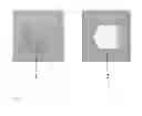
FIG. 1 is a drawing of a group III nitride wafer of present invention.
-
- In the figure each number represents the followings:
- The first layer
- 1a. The surface of the first layer
- The second layer
- 2a. The surface of the second layer
- 3. The third layer
FIG. 2 is a typical process flow to fabricate a group III nitride wafer of present invention.
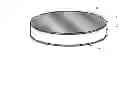
FIG. 3 is a picture of GaN wafer after H3PO4 etching.
-
- In the figure each number represents the followings:
- 1. Ga-face (+polar surface)
- 2. N-face (−polar surface)
DETAILED DESCRIPTION OF THE INVENTION
Overview
The group III nitride wafer of the present invention provides a wafer having one surface visually distinguishable from the other surface. The group III nitride wafer is suitable for fabricating various optoelectronic and electronic devices. Unlike the wafer fabrication method using vapor phase epitaxy, bulk crystals of group III nitride such as GaN, AlN, InN or alloy of such group III nitride are grown with a bulk growth method such as ammonothermal growth. Then, group III nitride wafers are sliced from a bulk crystal with a mechanical means such as a multiple wire saw. After the slicing, the both surfaces of the wafer looks almost identical because the surfaces become rough from the mechanical process. To identify one surface from the other surface, the wafers are chemically etched. After an appropriate chemical etching, one surface of the wafer can be visually distinguished from the other surface.
To fabricate a group III nitride wafer suitable for successive device fabrication, one surface of the wafer is polished. The present invention makes it possible to visually identify the surface which should be polished so that a mistake to process a wrong surface can be avoided.
Technical Description of the Invention
The current invention presents a group III nitride wafer with one surface visually distinguishable from the other side so that the further polishing process will be conducted without a mistake of processing a wrong side. FIG. 1 presents one example of the current invention. A wafer-shaped layer of highly oriented poly or single crystalline group III nitride (3) is sandwiched between the first layer (1) and the second layer (2) created when the wafer is cut from an ingot using a saw or laser, for instance. The wafer is chemically etched so that the surface of the first layer (1a) is visually distinguishable from the surface of the second layer (2a). One surface is typically distinguished from the other surface with the difference of roughness, reflectivity of light or color.
Group III nitride crystal in the common phase has a wurtzite structure and the crystal is polar along the c-axis. If group III nitride wafers sliced from a group III nitride bulk crystal have c-plane orientation (wafers sliced perpendicular to the c-axis) or semipolar orientation (wafers sliced not parallel nor perpendicular to the c-axis), the wafer has a polarity. i.e. one surface is +polar (or group III face) and the other surface is −polar (or N face). Even nonpolar a- or m-plane with large enough miscut can become polar. Since the chemical, electrical, physical, mechanical, and/or optical properties on the +polar surface are different from those on the −polar surface, it is very important to process a correct surface for a device fabrication. However, after the slicing process, the both surfaces look almost identical because the slicing is conducted through a mechanical means. An appropriate etch such as chemical etching creates one surface visually different from the other surface; thus removing ambiguity of which surface the further process must be conducted on.
FIG. 2 presents one example of methods to fabricate the wafer in the current invention. First, a bulk crystal of group III nitride such as GaN is grown by a bulk growth method such as ammonothermal growth, flux growth or high-pressure solution growth. Then, wafers of preferred orientation are sliced from the group III nitride bulk crystal with e.g. a mechanical means such as a multiple wire saw. After the slicing, both surfaces of the wafers become rough due to the mechanical damage of slicing. This surface damage layers of the wafers can be polycrystalline phase and/or amorphous phase due to the damage. Because of this mechanical or heat damage, both surfaces look almost identical even though the wafers have polarity. Then, the wafers are etched a sufficient amount to make one surface visually distinguishable from the other surface. Etching can be conducted with acid, base or other kind of wet or dry etchant. If necessary the temperature of the etching agent can be elevated to accelerate the process. Etching may remove some or all of a damaged layer. Either the group III polar face of one layer or the N-polar face of the other layer may be etched. Also, both the first and second layer may be etched as long as the surface appearance of the two layers becomes different.
Example 1
Bulk crystal of GaN was grown on a GaN seed crystal with an ammonothermal method using polycrystalline GaN as a nutrient, supercritical ammonia as a solvent, and sodium (5 mol % to ammonia) as a mineralizer. The temperature was between 500 to 550 C and pressure was between 170 and 240 MPa. The thickness of the crystal was 6.9 mm and the surface area was approximately 100 mm2. A full-width half maximum (FWHM) of the X-ray diffraction from 002 plane was 900 arcsec. From this FWHM number, we estimate the density of line defects and grain boundaries is less than 106 cm−2. Although the crystal was not characterized with an optical and electrical measurement, those characteristics are expected to be the typical one for bulk crystal of GaN. For example, photoluminescence or cathode luminescence is expected to show luminescence from band-edge emission at around 370 nm, blue emission at around 400 nm, and/or yellow luminescence at around 600 nm. Conductivity type is expected to be n−type or n+type with carrier concentration from 1017 to 1020 cm−3. Optical absorption coefficient of such crystal is expected to be 50 cm−1 or less. The lattice constant of the crystal was 51.84790 nm for c-lattice and 31.89343 nm for a-lattice. The lattice constant for GaN can change within 10% depending of growth conditions.
The crystal was sliced into c-plane wafers with a multiple wire saw. The wafer thickness was approximately 500 microns and 8 wafers were fabricated from this particular crystal. We can produce wafers of different thickness by changing the wire pitch. Also, if the crystal is thicker or the wire is thinner, we can obtain more wafers. After the slicing, both surfaces of the wafers looked very similar due to surface damage. The sliced wafers were placed in wafer carriers. Then, the wafers in the carriers were immersed in acetone in an ultrasonic bath to remove diamond slurry and organic substances from the wafers. Acetone cleaning in the ultrasonic bath was repeated until the diamond slurry and organic substances were completely removed. If necessary, the surface of the wafers can be wiped with fibrous wiper. Then, the wafers in the carrier were immersed in isopropanol in an ultrasonic bath to remove acetone followed by a rinse with de-ionized water. After lightly drying the wafers in the carriers with air blower or in a baking oven, the wafers in the carrier were immersed in 85 wt % H3PO4 at 190° C. for 30 seconds. Then, the wafers were rinsed with de-ionized water. After the etching, N face (−polar surface) became shiny due to the chemical etching whereas the Ga face (+polar surface) did not change its appearance. As shown in FIG. 3 the Ga face does not reflect light well whereas the N face reflects light well so that the surface is visually distinguishable.
Although the details of the surfaces on both wafers were not analyzed, etching of N face is likely to occur because the surface was damaged from the cutting process mechanically and/or with heat (i.e. slicing). Thus, the etching technique of this invention preferably utilizes a mechanical process to cut a wafer from an ingot prior to a preferred chemical etch process. The chemical etching may also be effective to fully or partially remove the damaged layer of group III nitride wafers.
High quality GaN wafers having a surface suitable for device fabrication can be prepared by grinding, lapping, and polishing the Ga face or N face of the wafer. Due to the different appearance of the surface, a mistake to polish a wrong surface will be greatly reduced, which improves production yield.
Advantages and Improvements
The current invention provides a group III nitride wafers having one side visually distinguishable from the other side. Since the transition from the slicing process to the polishing process involves re-mounting of wafers, it is very important to make each surface visually distinguishable from the other. The group III nitride wafer of the current invention will improve the overall production yield of group III nitride wafer such as GaN.
Possible Modifications
Although the preferred embodiment describes GaN substrates, the substrate can be group III nitride alloys of various composition, such as AlN, AlGaN, InN, InGaN, or GaAlInN
Although the preferred embodiment describes ammonothermal growth as a bulk growth method, other growth methods such as high-pressure solution growth, flux growth, hydride vapor phase epitaxy, physical vapor transport, or sublimation growth can be used.
Although the preferred embodiment describes c-plane wafers, the invention is applicable to other orientations such as semipolar planes including 10-1-1 plane, 20-2-1 plane, 11-21 plane, and 11-22 plane. Also, the invention is applicable to wafers with misorientation from a basal plane (such as c-plane, m-plane, a-plane and semipolar planes) as long as the wafer has +polar (Ga face) and −polar (N face) surface.
Although the preferred embodiment describes slicing with a multiple wire saw, other slicing method such as an inner blade saw, an outer blade saw and a single wire saw can also be used. In addition, the current invention is also applicable to other mechanical process such as grinding and thinning
Although the preferred embodiment describes etching with heated phosphoric acid, other acidic etching agent such as hydrochloric acid, sulfuric acid, nitric acid, hydrofluoric acid, and mixture of them may be used. Also basic etching agent such as sodium hydroxide, potassium hydroxide, aqueous solution of them, anhydrous solution of them and eutectic solution of them may be used. In addition, other etching agent such as hydrogen peroxide, iodine-based solutions may be used as long as one surface become visually distinguishable from the other surface.
Consequently, what is disclosed by way of example and not by way of limitation is the following:
-
- 1. A group III nitride wafer having composition of GaxAlyIn1-x-yN (0≦x≦1, 0≦x+y≦1), wherein the both surfaces are roughened from a mechanical process and the surfaces are chemically treated to visually distinguish one surface from another.
- 2. A group III nitride wafer according to paragraph 1, wherein the mechanical process comprises slicing the wafer from a bulk crystal of group III nitride.
- 3. A group III nitride wafer according to paragraph 1, wherein the mechanical process is grinding of the wafer.
- 4. A group III nitride wafer in any of claims 1-2, wherein the wafer was sliced from a bulk crystal of group III nitride with a multiple wire saw.
- 5. A group III nitride wafer according to paragraphs 1 through 4, wherein the chemical treatment is etching.
- 6. A group III nitride wafer according to paragraph 5, wherein the etching is performed using a wet etchant.
- 7. A group III nitride wafer according to paragraph 6, wherein the wet etchant comprises phosphoric acid.
- 8. A group III nitride wafer according to paragraphs 1 through 7, wherein the chemical treatment is etching in phosphoric acid or its mixture at 50° C. or higher.
- 9. A group III nitride wafer according to paragraphs 1 through 8, wherein the orientation is c-plane with misorientation from minus 10 degree to plus 10 degree.
- 10. A group III nitride wafer according to paragraphs 1 through 8, wherein the orientation is a semipolar plane with misorientation from minus 10 degree to plus 10 degree.
- 11. A group III nitride wafer according to paragraphs 1 through 8, wherein the orientation is a nonpolar plane with misorientation from minus 10 degree to minus 0.1 degree or plus 0.1 degree to plus 10 degree.
- 12. A group III nitride wafer according to paragraphs 1 through 11, wherein the surface area is more than 100 mm2.
- 13. A group III nitride wafer according to paragraphs 1 through 12, wherein the composition is GaN.
- 14. A group III nitride wafer comprising a first layer and a second layer of damaged group III nitride on opposite faces of a third layer of highly oriented poly or single crystalline group III nitride, wherein the first and the second layer were formed through a mechanical process and the surface of the second layer is made visually distinguishable from the surface of the first layer by a chemical etching.
- 15. A group III nitride wafer according to paragraph 14, wherein the wafer is sliced from a bulk crystal of group III nitride.
- 16. A group III nitride wafer according to paragraph 14 and claim 15, wherein the wafer is sliced from a bulk crystal of group III nitride with a multiple wire saw.
- 17. A group III nitride wafer according to paragraphs 14 through 16, wherein the chemical etching uses acid or base.
- 18. A group III nitride wafer according to paragraph 17, wherein the chemical etching uses phosphoric acid or its mixture.
- 19. A group III nitride wafer according to paragraph 17 and claim 18, wherein the chemical etching uses phosphoric acid or its mixture at 50° C. or higher.
- 20. A group III nitride wafer according to paragraph 14 through 19, wherein the surface area of the wafer is more than 100 mm2.
- 21. A group III nitride wafer according to paragraph 14 through 20, wherein the density of line defect and grain boundary of the third layer is less than 106 cm−2.
- 22. A group III nitride wafer according to paragraphs 14 through 21, wherein the group III nitride is GaN.
- 23. A method of fabricating a group III nitride wafer having a first layer and a second layer, each comprising a damaged or partially damaged layer of group III nitride, and a third layer having highly oriented poly or single crystalline group III nitride, comprising:
- (a) slicing a wafer from a bulk crystal of a group III nitride ingot mechanically;
- (b) chemically etching the wafer under conditions that make the surface of the second layer visually distinguishable from the surface of the first layer.
- 24. A method according to paragraph 23, wherein the wafer is cut from the ingot using a multiple wire saw.
- 25. A method according to paragraph 23 or paragraph 24, wherein the chemical etching uses phosphoric acid or its mixture.
- 26. A method according to any of paragraphs 23 through 25, wherein the chemical etching uses phosphoric acid or its mixture at 50° C. or higher.
- 27. A method according to any of paragraphs 23 through 26, wherein the density of line defect and grain boundary of the third layer is less than 106 cm−2.
- 28. A method according to any of paragraphs 23 through 27, wherein the group III nitride is GaN.
- 29. A method of fabricating a group III nitride wafer according to paragraph 28 and including the step of growing a bulk crystal of group III nitride to form the ingot, wherein the growth of bulk crystal of group III nitride uses supercritical ammonia and comprises the following steps:
- (a) charging Ga-containing nutrient in a high-pressure reactor;
- (b) charging at least one seed crystal in the high-pressure reactor;
- (c) charging a chemical additive which increases dissolution of Ga-containing nutrient into the supercritical ammonia;
- (d) charging ammonia in the high-pressure reactor;
- (e) sealing the high-pressure ammonia;
- (f) providing enough heat to ammonia to create supercritical state;
- (g) dissolving the Ga-containing nutrient into the supercritical ammonia;
- (h) crystallizing GaN on the seed crystal.
- 30. A method of fabricating a group III nitride wafer comprising removing the first layer or the second layer of a wafer of any of paragraphs 14 through 22 and exposing the third layer with a surface quality sufficient to fabricate devices.
- 31. A method according to paragraph 30, wherein the removing process comprises grinding.
- 32. A method according to paragraph 30, wherein the removing process comprises lapping.
- 33. A method according to paragraph 30, wherein the removing process comprises polishing.
- 34. A method according to paragraph 30, wherein the removing process comprises chemical mechanical polishing.
- 35. A method according to any of paragraphs 30 through 34, wherein the group III nitride is GaN.
REFERENCES
The following references are incorporated by reference herein:
- [1] R. Dwiliński, R. Doradziński, J. Garczyński, L. Sierzputowski, Y. Kanbara, U.S. Pat. No. 6,656,615.
- [2] R. Dwiliński, R. Doradziński, J. Garczyński, L. Sierzputowski, Y. Kanbara, U.S. Pat. No. 7,132,730.
- [3] R. Dwiliński, R. Doradziński, J. Garczyński, L. Sierzputowski, Y. Kanbara, U.S. Pat. No. 7,160,388.
- [4] K. Fujito, T. Hashimoto, S, Nakamura, International Patent Application No. PCT/US2005/024239, WO07008198.
- [5] T. Hashimoto, M. Saito, S, Nakamura, International Patent Application No. PCT/US2007/008743, WO07117689. See also US20070234946, U.S. application Ser. No. 11/784,339 filed Apr. 6, 2007.
- [6] D'Eyelyn, U.S. Pat. No. 7,078,731.
- [7]. S. Porowski, MRS Internet Journal of Nitride Semiconductor, Res. 4S1, (1999) G1.3.
- [8] T. Inoue, Y. Seki, O. Oda, S. Kurai, Y. Yamada, and T. Taguchi, Phys. Stat. Sol. (b), 223 (2001) p. 15.
- [9] M. Aoki, H. Yamane, M. Shimada, S. Sarayama, and F. J. DiSalvo, J. Cryst. Growth 242 (2002) p. 70.
- [10] T. Iwahashi, F. Kawamura, M. Morishita, Y. Kai, M. Yoshimura, Y. Mori, and T. Sasaki, J. Cryst Growth 253 (2003) p. 1.
Claims
What is claimed is:1. A method of fabricating a group III nitride wafer having a first layer and a second layer, each comprising a damaged or partially damaged layer of group III nitride, and a third layer having highly oriented poly or single crystalline group III nitride, comprising:
(a) slicing a wafer from a bulk crystal of a group III nitride ingot mechanically;
(b) chemically etching the wafer under conditions that make the surface of the second layer visually distinguishable from the surface of the first layer.
2. A method according to claim 1, wherein the wafer is cut from the ingot using a multiple wire saw.
3. A method according to claim 1, wherein the chemical etching uses phosphoric acid or its mixture.
4. A method according to claim 1, wherein the chemical etching uses phosphoric acid or its mixture at 50° C. or higher.
5. A method according to claim 1, wherein the density of line defect and grain boundary of the third layer is less than 106 cm−2.
6. A method according to claim 1, wherein the group III nitride comprises GaN.
7. A method according to claim 6 and including the step of growing a bulk crystal of group III nitride to form the ingot, wherein the growth of bulk crystal of group III nitride uses supercritical ammonia and comprises the following steps:
(a) charging Ga-containing nutrient in a high-pressure reactor;
(b) charging at least one seed crystal in the high-pressure reactor;
(c) charging a chemical additive which increases dissolution of Ga-containing nutrient into the supercritical ammonia;
(d) charging ammonia in the high-pressure reactor;
(e) sealing the high-pressure ammonia;
(f) providing enough heat to ammonia to create supercritical state;
(g) dissolving the Ga-containing nutrient into the supercritical ammonia;
(h) crystallizing GaN on the seed crystal.
8. A method of fabricating a group III nitride wafer comprising removing the first layer or the second layer of a wafer of claim 1 and exposing the third layer with a surface quality sufficient to fabricate devices.
9. A method according to claim 8, wherein the removing process comprises grinding.
10. A method according to claim 8, wherein the removing process comprises lapping.
11. A method according to claim 8, wherein the removing process comprises polishing.
12. A method according to claim 8, wherein the removing process comprises chemical mechanical polishing.
13. A method according to claim 8, wherein the group III nitride comprises GaN.
Images & Drawings included:
Sources:
- United States Patent and Trademark Office - verify current appl. status at the USPTO↗
Similar patent applications:
- » 20140054589
Bismuth-doped semi-insulating group III nitride wafer and its production method - » 20140061662
Group III nitride wafer and its production method - » 20160130720
Bismuth-doped semi-insulating group III nitride wafer and its production method - » 20050227453
Group III nitride semiconductor crystal, production method thereof and group III nitride semiconductor epitaxial wafer
Recent applications in this class:
- » 20250063787 2025-02-20
NITRIDE SEMICONDUCTOR DEVICE COMPRISING LAYERED STRUCTURE OF ACTIVE REGION AND METHOD FOR MANUFACTURING THE SAME - » 20250063786 2025-02-20
NITRIDE SEMICONDUCTOR SUBSTRATE AND METHOD FOR PRODUCING SAME - » 20250056858 2025-02-13
GROUP III-NITRIDE SEMICONDUCTOR STRUCTURE ON SILICON-ON-INSULATOR AND METHOD OF GROWING THEREOF - » 20250040212 2025-01-30
NITRIDE SEMICONDUCTOR DEVICE - » 20250031425 2025-01-23
FIELD ASSISTED INTERFACIAL DIFFUSION DOPING THROUGH HETEROSTRUCTURE DESIGN - » 20250022921 2025-01-16
NITRIDE SEMICONDUCTOR DEVICE - » 20250015142 2025-01-09
SEMICONDUCTOR DEVICE - » 20250006798 2025-01-02
NITRIDE SEMICONDUCTOR DEVICE AND MANUFACTURING METHOD THEREFOR - » 20240421195 2024-12-19
NITRIDE SEMICONDUCTOR DEVICE - » 20240421194 2024-12-19
GALLIUM NITRIDE DEVICE WITH ARTIFICIAL FIELD PLATES
Recent applications for this Assignee:
- » 20230163724 2023-05-25
Terahertz Gunn oscillator using gallium nitride - » 20210355598 2021-11-18
Low-dislocation bulk GaN crystal and method of fabricating same - » 20190096668 2019-03-28
Seed crystal for growth of gallium nitride bulk crystal in supercritical ammonia and fabrication method - » 20190096667 2019-03-28
Seed crystal for growth of gallium nitride bulk crystal in supercritical ammonia and fabrication method - » 20190093256 2019-03-28
Seed crystal for growth of gallium nitride bulk crystal in supercritical ammonia and fabrication method - » 20180182882 2018-06-28
Electronic device using group III nitride semiconductor and its fabrication method - » 20180182881 2018-06-28
Electronic device using group III nitride semiconductor and its fabrication method - » 20180182873 2018-06-28
Electronic device using group III nitride semiconductor and its fabrication method - » 20180182872 2018-06-28
Electronic device using group III nitride semiconductor and its fabrication method - » 20160376727 2016-12-29
High pressure reactor and method of growing group III nitride crystals in supercritical ammonia